Paper Sharing
【International Papers】DC Modeling of 8 kV Depletion Mode Gallium Oxide MOSFET
日期:2026-06-03阅读:104
Researchers from the University of Arkansas have published a dissertation titled “DC Modeling of 8 kV Depletion Mode Gallium Oxide MOSFET“ in IEEE Electron Device Letters (IEEE Applied Power Electronics Conference and Exposition, APEC).
Background
Gallium oxide (Ga₂O₃) has attracted significant attention for high‑voltage power electronics due to its ultra‑wide bandgap, high critical electric field (~8 MV/cm), and cost‑effective single‑crystal wafer production. Among its polymorphs, β‑Ga₂O₃ is the most stable and has enabled 8 kV depletion‑mode lateral MOSFETs. Based on the authors’ previous work on 750 V β‑Ga₂O₃ MOSFET modeling, this paper extends the physics‑based compact modeling approach to higher‑voltage devices for power electronic circuit simulation and design.
Abstract
Gallium oxide (Ga₂O₃) has recently gained significant attention for high‑voltage power electronics owing to its ultra‑wide bandgap, high critical electric field (~8 MV/cm), and the potential for cost‑effective single‑crystal wafer production. Among its polymorphs, β‑Ga₂O₃ is the most stable and has enabled the demonstration of depletion‑mode lateral MOSFETs with breakdown voltages up to 8 kV. Building on our recent work on a 750 V β‑Ga₂O₃ MOSFET, this paper extends a physics‑based compact modeling approach to higher‑voltage devices. The model formulation combines channel current with drift resistance, where drift mobility is extracted from Hall mobility accounting for four dominant scattering mechanisms and their temperature dependence. Simulation results show good agreement with measured transfer and output characteristics, validating the model’s scalability across voltages. This compact model provides a physics‑informed framework for incorporating Ga₂O₃ devices into power electronic circuit simulation and design.
Highlights
First extended physics‑based compact modeling from 750 V to 8 kV high‑voltage β‑Ga₂O₃ depletion‑mode MOSFET.
Mobility model considers four scattering mechanisms (polar optical phonon, ionized impurity, acoustic deformation potential, neutral impurity) and temperature dependence.
Adopts dual‑channel current formulation for accurate fitting in low and high drain current regions with smooth linear‑to‑saturation transition.
Performs TCAD simulation for C‑V characteristics extraction and reveals field‑plate effects on electric field, leakage, and depletion region.
Simulation agrees well with experiments; the model is scalable over wide voltages and ready for circuit design.
Conclusion
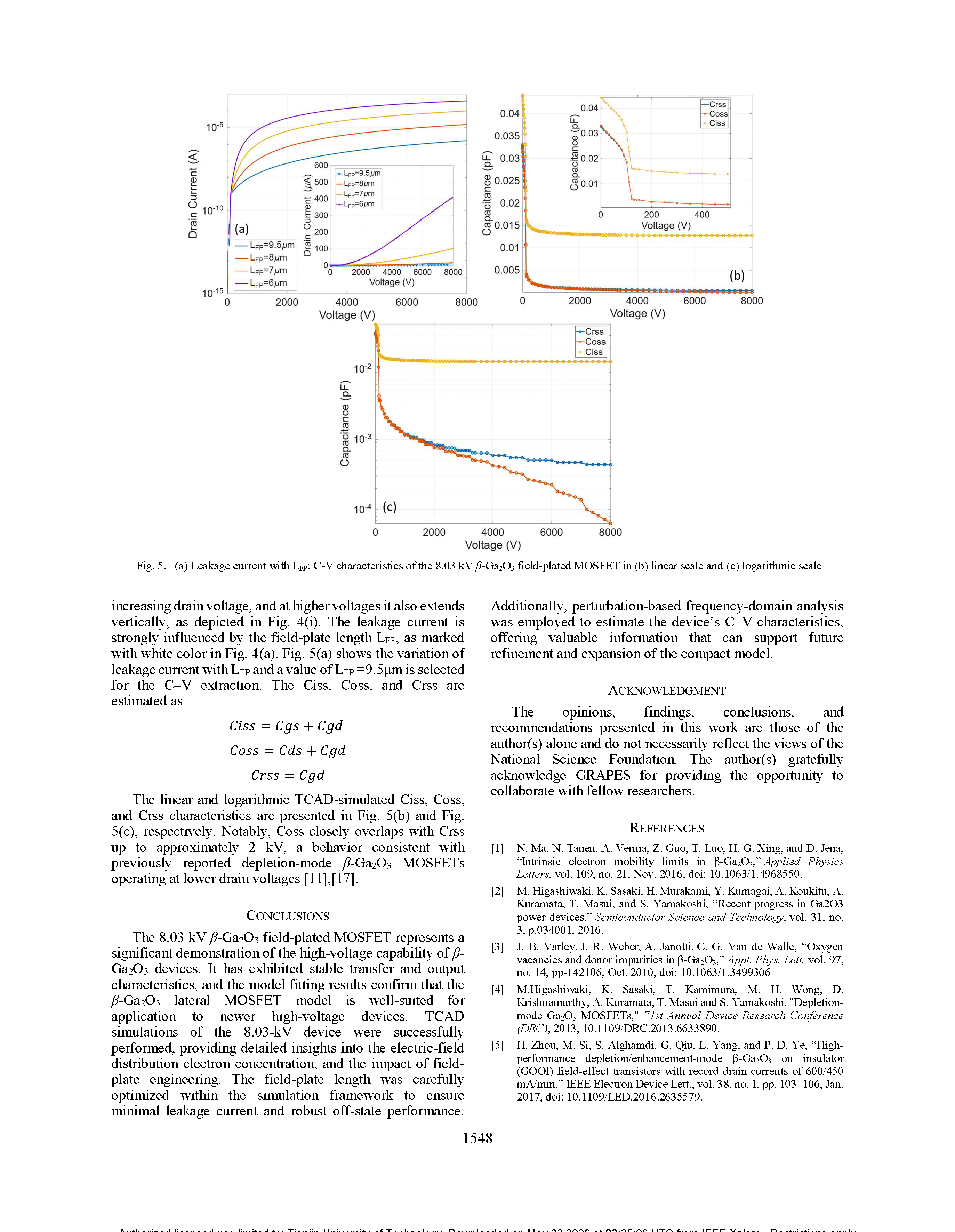
The 8.03 kV β‑Ga₂O₃ field‑plated MOSFET represents a significant demonstration of the high‑voltage capability of β‑Ga₂O₃ devices. It has exhibited stable transfer and output characteristics, and the model fitting results confirm that the β‑Ga₂O₃ lateral MOSFET model is well‑suited for application to newer high‑voltage devices. TCAD simulations of the 8.03‑kV device were successfully performed, providing detailed insights into the electric‑field distribution, electron concentration, and the impact of field‑plate engineering. The field‑plate length was carefully optimized within the simulation framework to ensure minimal leakage current and robust off‑state performance. Additionally, perturbation‑based frequency‑domain analysis was employed to estimate the device’s C–V characteristics, offering valuable information that can support future refinement and expansion of the compact model.
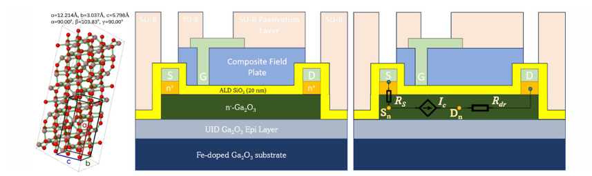
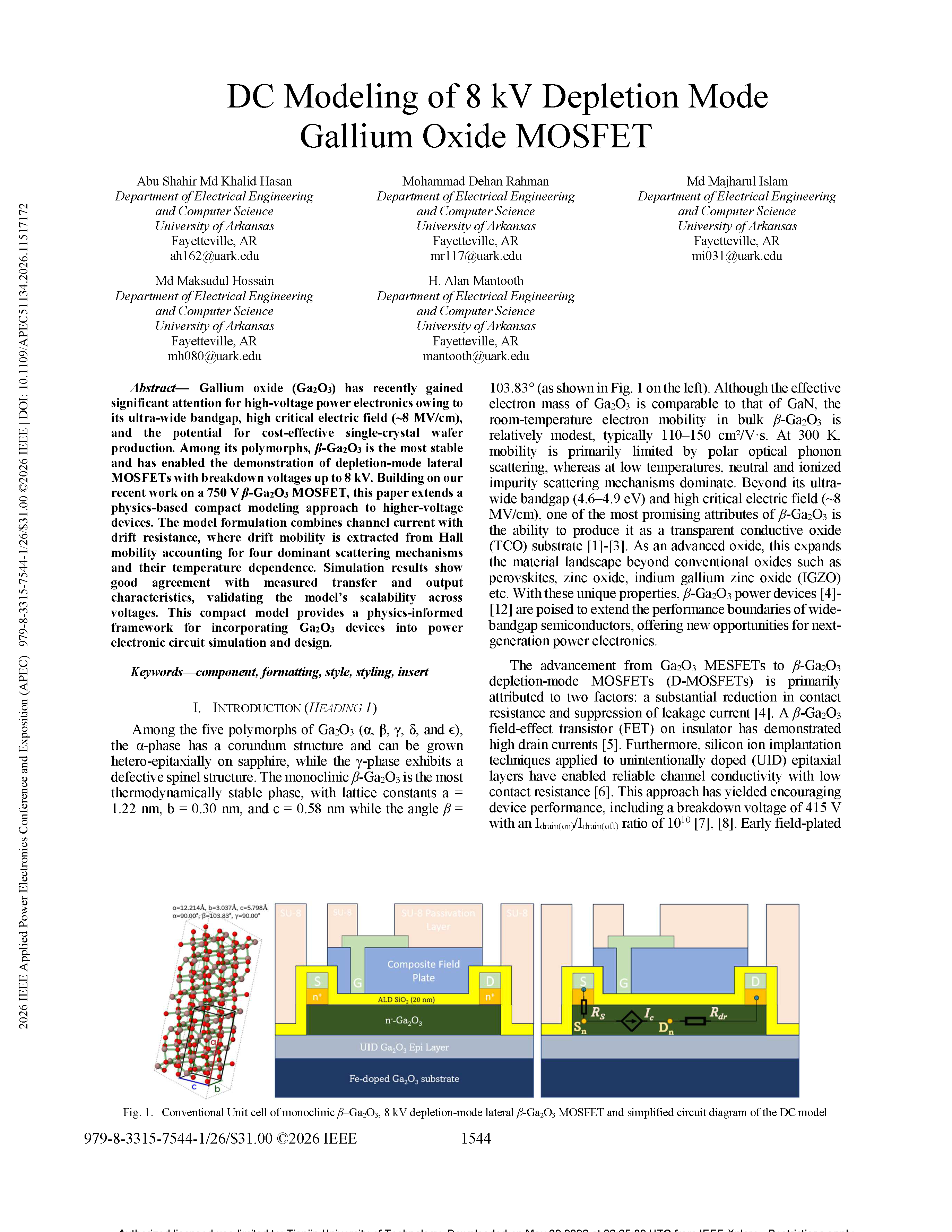
Figure 1 Conventional Unit cell of monoclinic β-Ga₂O₃, 8 kV depletion-mode lateral β-Ga₂O₃ MOSFET and simplified circuit diagram of the DC model
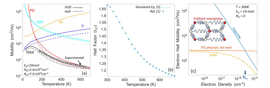
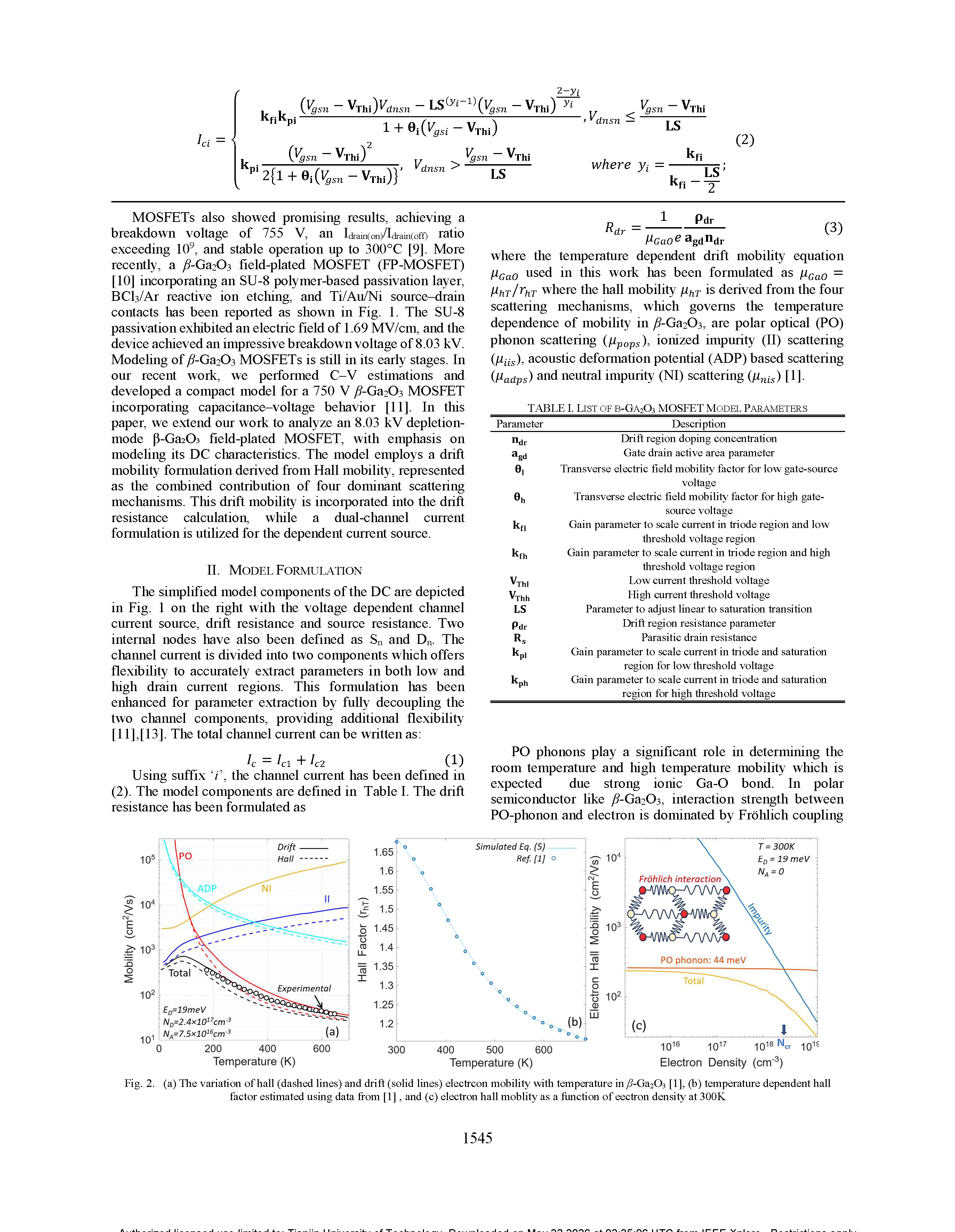
Figure 2 (a) The variation of hall (dashed lines) and drift (solid lines) electron mobility with temperature in β-Ga₂O₃, (b) temperature dependent hall factor estimated, and (c) electron hall mobility as a function of electron density at 300K
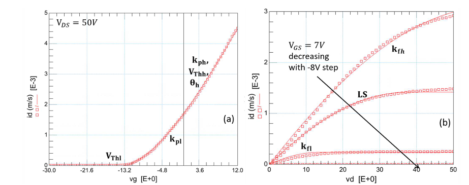
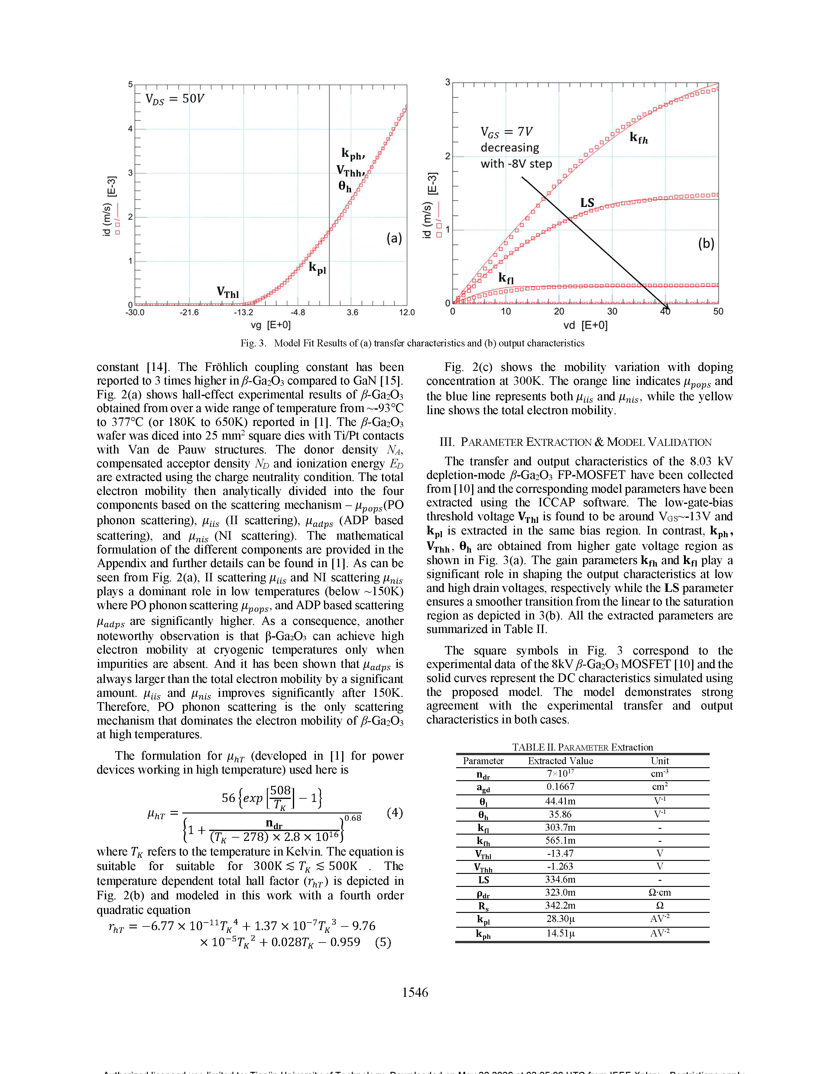
Figure 3 Model Fit Results of (a) transfer characteristics and (b) output characteristics
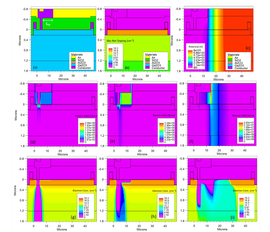
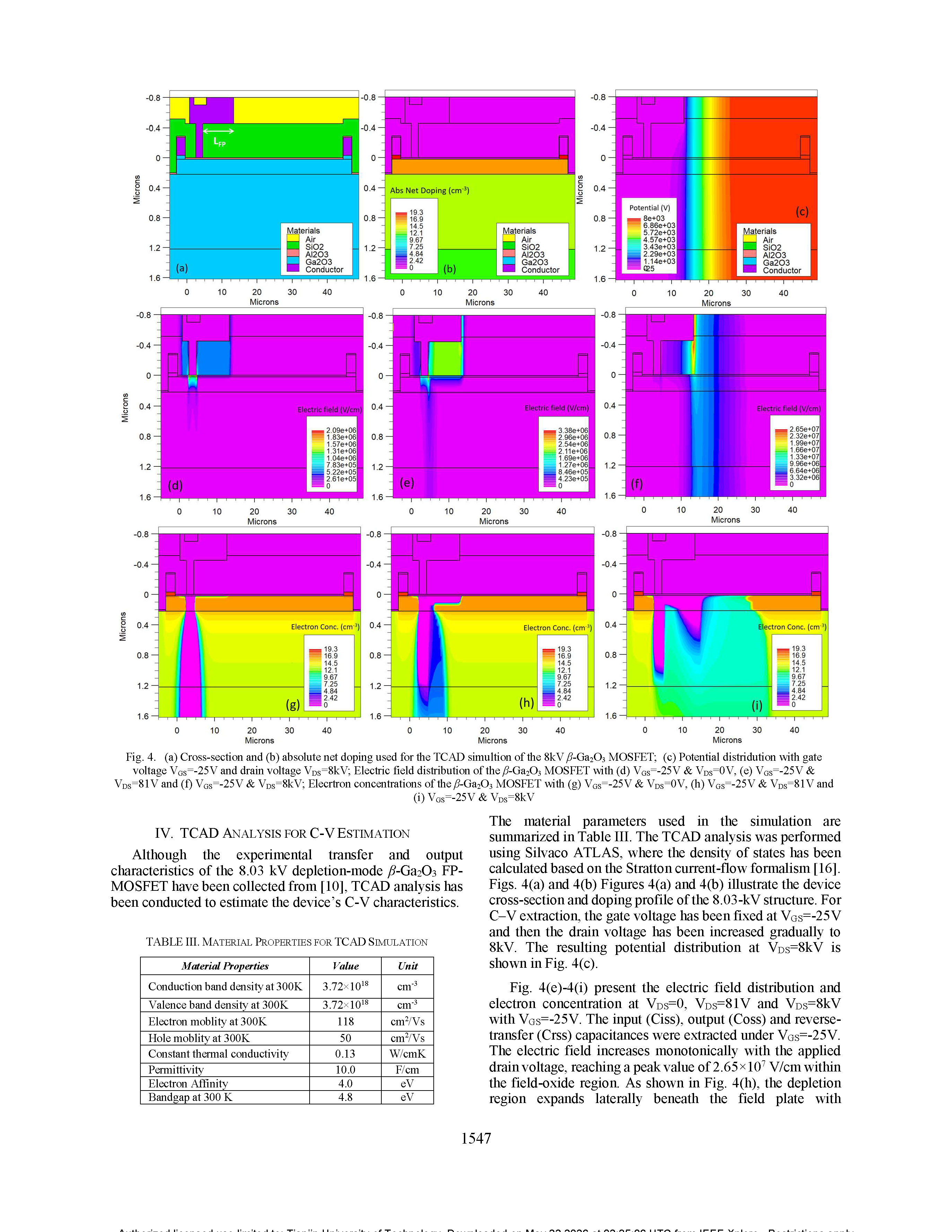
Figure 4 (a) Cross-section and (b) absolute net doping used for the TCAD simulation of the 8 kV β-Ga₂O₃ MOSFET; (c) Potential distribution with gate voltage VGS=-25 V and drain voltage VDS=8 kV; Electric field distribution of the β-Ga₂O₃ MOSFET with (d) VGS=-25 V & VDS=0 V, (e) VGS=-25 V & VDS=81 V and (f) VGS=-25 V & VDS=8 kV; Electron concentrations of the β-Ga₂O₃ MOSFET with (g) VGS=-25 V & VDS=0 V, (h) VGS=-25 V & VDS=81 V and (i) VGS=-25 V & VDS=8 kV
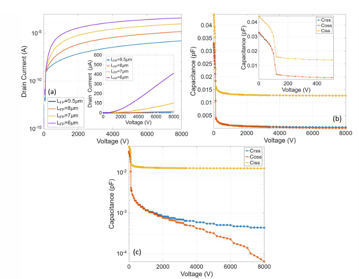
Figure 5 (a) Leakage current with LFP; C-V characteristics of the 8.03 kV β-Ga₂O₃ field-plated MOSFET in (b) linear scale and (c) logarithmic scale
DOI:
10.1109/APEC51134.2026.11517172