Paper Sharing
【Member Papers】Effective etching of (010) β-Ga₂O₃ with molten KOH + NaOH for defects identification
日期:2026-06-03阅读:118
Researchers from Zhejiang University have published a dissertation titled " Effective etching of (010) β-Ga₂O₃ with molten KOH + NaOH for defects identification " in Vacuum.
Background
β phase gallium oxide (β-Ga₂O₃) is an emerging ultrawide-bandgap semiconductor with great potential for high-power electronics and deep-ultraviolet photodetectors. Owing to its excellent optoelectronic properties, including a ultrawide bandgap of ~4.9 eV, a high critical breakdown electric field of 8 MV/cm, and an optical absorption edge near 260 nm. Structurally, β-Ga₂O₃ adopts a monoclinic crystal structure (space group C2/m), and the (010) plane is the only fundamental facet where the normal vector is consistent with the fundamental direction. This low-symmetry configuration gives the (010) surface distinct physicochemical behavior. For example, (010) oriented substrates perpendicular to the two primary cleavage planes (100) and (001), enable facile cleaving along those planes and possess the potential to exhibit excellent surface quality. Moreover, (010) plane shows the highest thermal conductivity in this anisotropic material. Combined with the high quality homoepitaxy achieved by techniques such as Metal Organic Chemical Vapor Deposition (MOCVD), Hydride Vapor Phase Epitaxy (HVPE) and Molecular Beam Epitaxy (MBE), these advantages have facilitated substantial progress in (010)-oriented power devices. However, the performance and yield of these devices are critically limited by crystalline defects, such as dislocations and nanopipes, which can lead to premature device failure and threshold voltage instability. Therefore, figuring out the nature and origin of these defects is essential for modifying crystal growth and device fabrication.
Abstract
The development of β-Ga₂O₃ for high-power electronics has been hampered by the longstanding challenge of characterizing defects on its (010) plane with conventional etchants. This study introduces a highly efficient molten alkali (NaOH + KOH) etching process that slashes the required time from 2 hours to just 2 minutes compared to typical hot H₃PO4 etching, producing clear, well-defined etch pits observable by optical microscopy. Crucially, this method could establish a definitive correlation between four distinct pit morphologies and specific defect types—including nanopipes, dislocations, mixed-type (dislocation + nanopipe), and strain-related defects—through systematic Focused Ion Beam-Transmission Electron Microscope (FIB‑TEM) analysis. The morphological evolution of nanopipe-related pits, depending on etching time, is also revealed. This work provides both a rapid characterization tool and fundamental insights critical for advancing β-Ga₂O₃ crystal growth and device performance.
Conclusion
In this study, a highly efficient defect characterization method for the β-Ga₂O₃ (010) plane via an optimized molten alkali etching process was developed. This approach successfully addresses the key Journal Pre-proof limitations of the conventional hot H3PO4 method by achieving three pivotal advancements: a significant reduction in process time (from 2 hours to 2 minutes), enabling direct defect observation under an optical microscope, and, most critically, producing distinct etch pit morphologies that serve as reliable indicators for specific defect types. Through FIB combined TEM establish definitive correlations between four characteristic pit shapes and their underlying defect types. Step-wise etching experiments further illuminated the morphological evolution of nanopipe-related defects. This research provides a reliable approach for the rapid and intuitive characterization of crystal defects on the β Ga₂O₃ (010) surface, holding significant importance for promoting the quality improvement of β Ga₂O₃ single crystals and their applications in power devices.
Project Support
This work was supported by the National Key Research and Development Program of China (2024YFE0205300), the National Natural Science Foundation of China (22205203), the Zhejiang Provincial Postdoctoral Research Project Excellence Funding (ZJ2024079), the Natural Science Foundation of Zhejiang (LZ25E070001), the National Program for Support of Topnotch Young Professionals, and the Leading Innovative and Entrepreneur Team Introduction Program of Hangzhou (TD2022012).
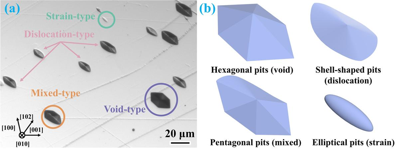
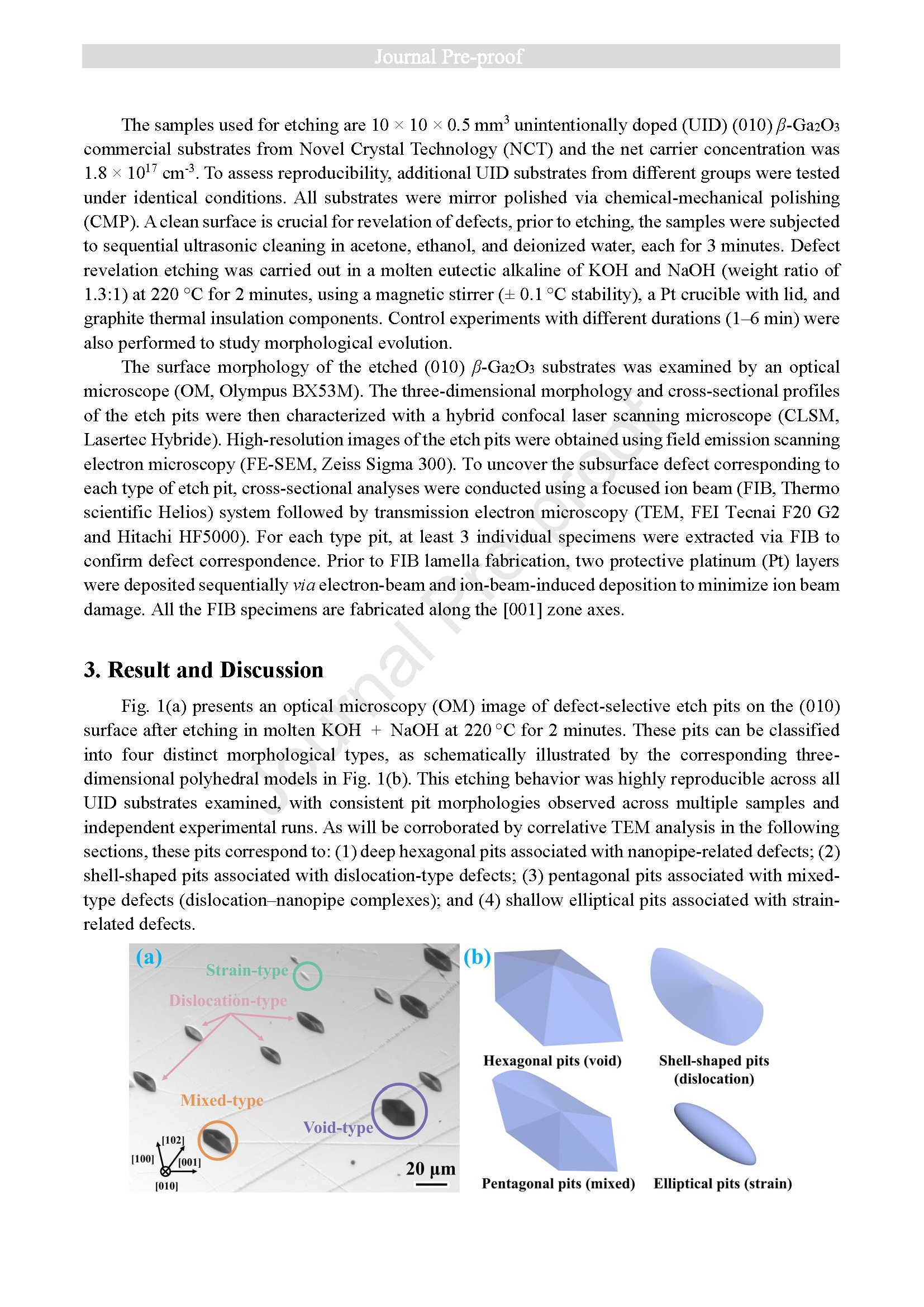
Fig. 1. (a) Optical microscope image of β-Ga₂O₃ (010) surface etched with molten KOH + NaOH at 220°C for 2 minutes; (b)Three-dimensional schematic models of the four types etch pits.
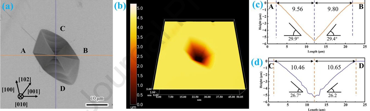
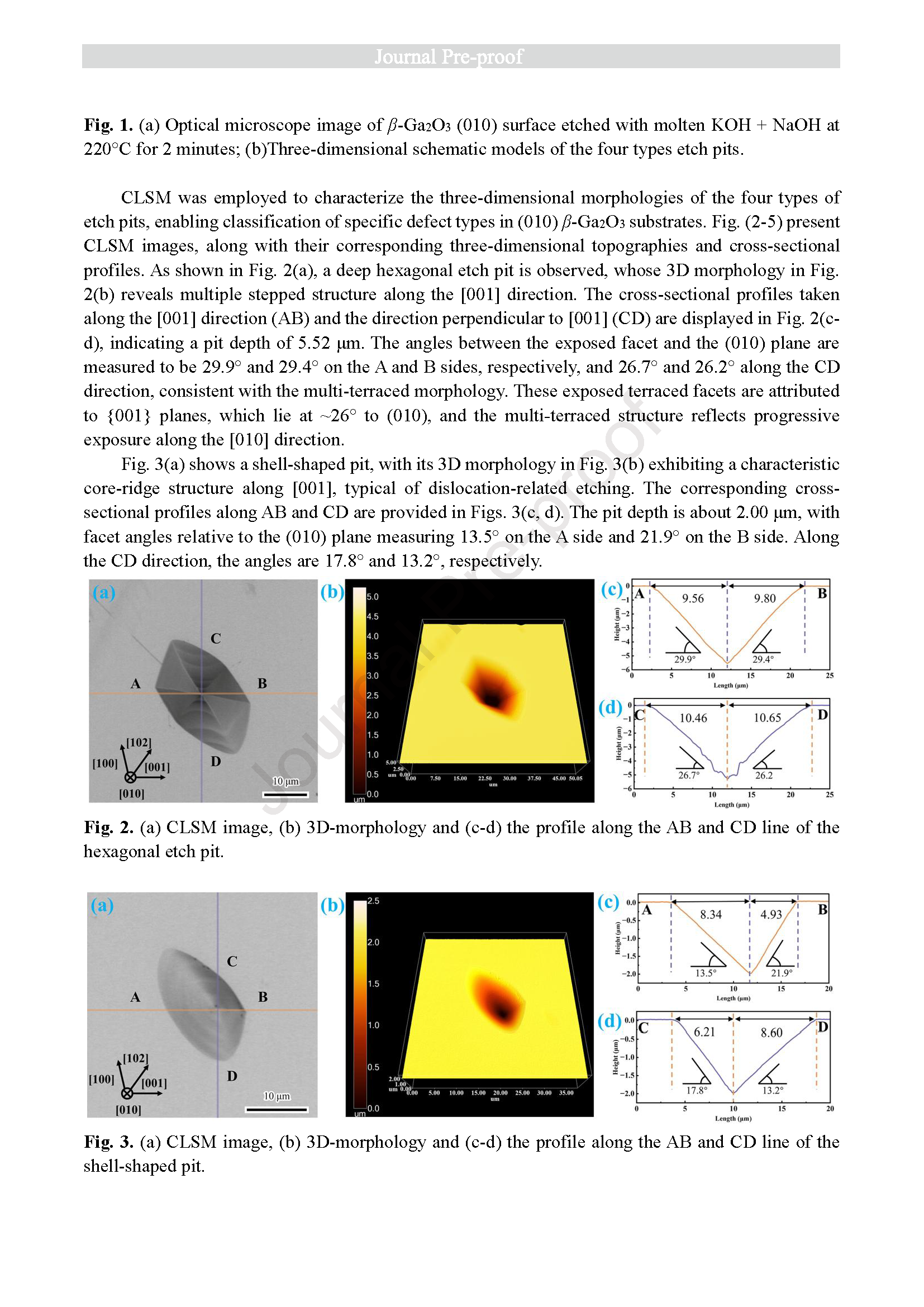
Fig. 2. (a) CLSM image, (b) 3D-morphology and (c-d) the profile along the AB and CD line of the hexagonal etch pit.
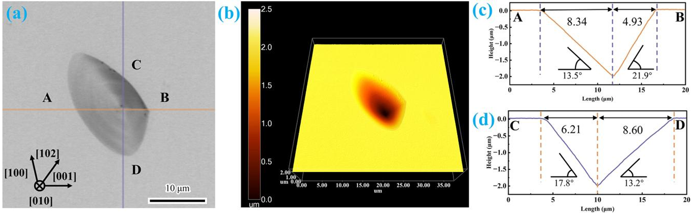
Fig. 3. (a) CLSM image, (b) 3D-morphology and (c-d) the profile along the AB and CD line of the shell-shaped pit.
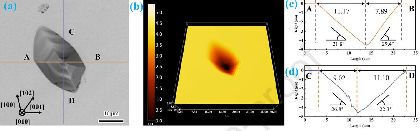
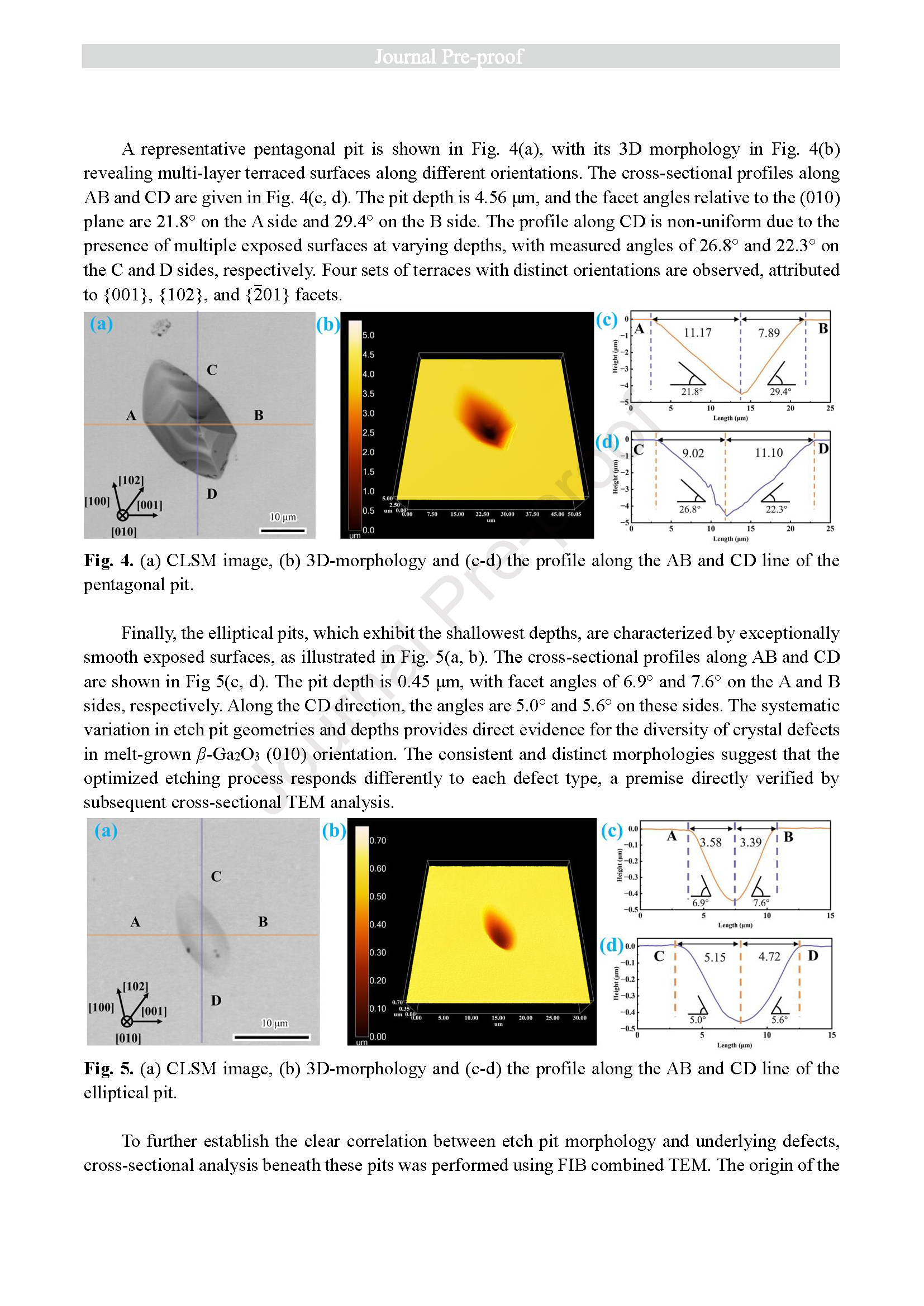
Fig. 4. (a) CLSM image, (b) 3D-morphology and (c-d) the profile along the AB and CD line of the pentagonal pit.
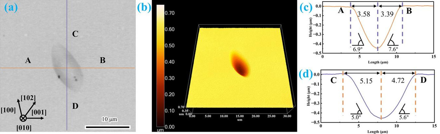
Fig. 5. (a) CLSM image, (b) 3D-morphology and (c-d) the profile along the AB and CD line of the elliptical pit.
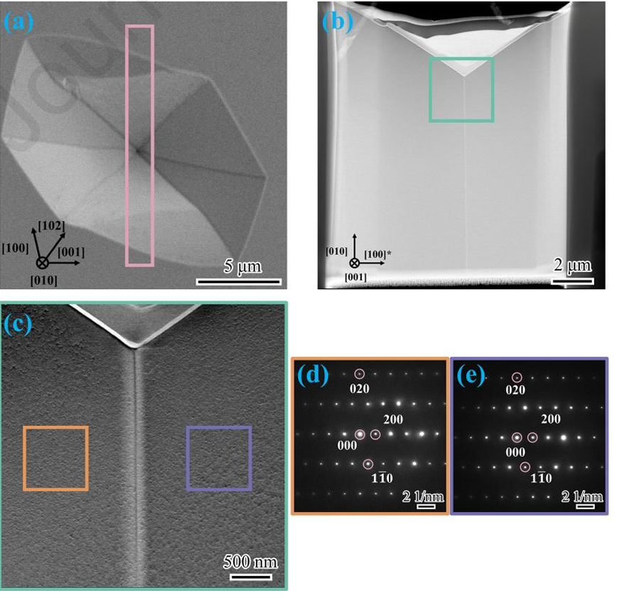
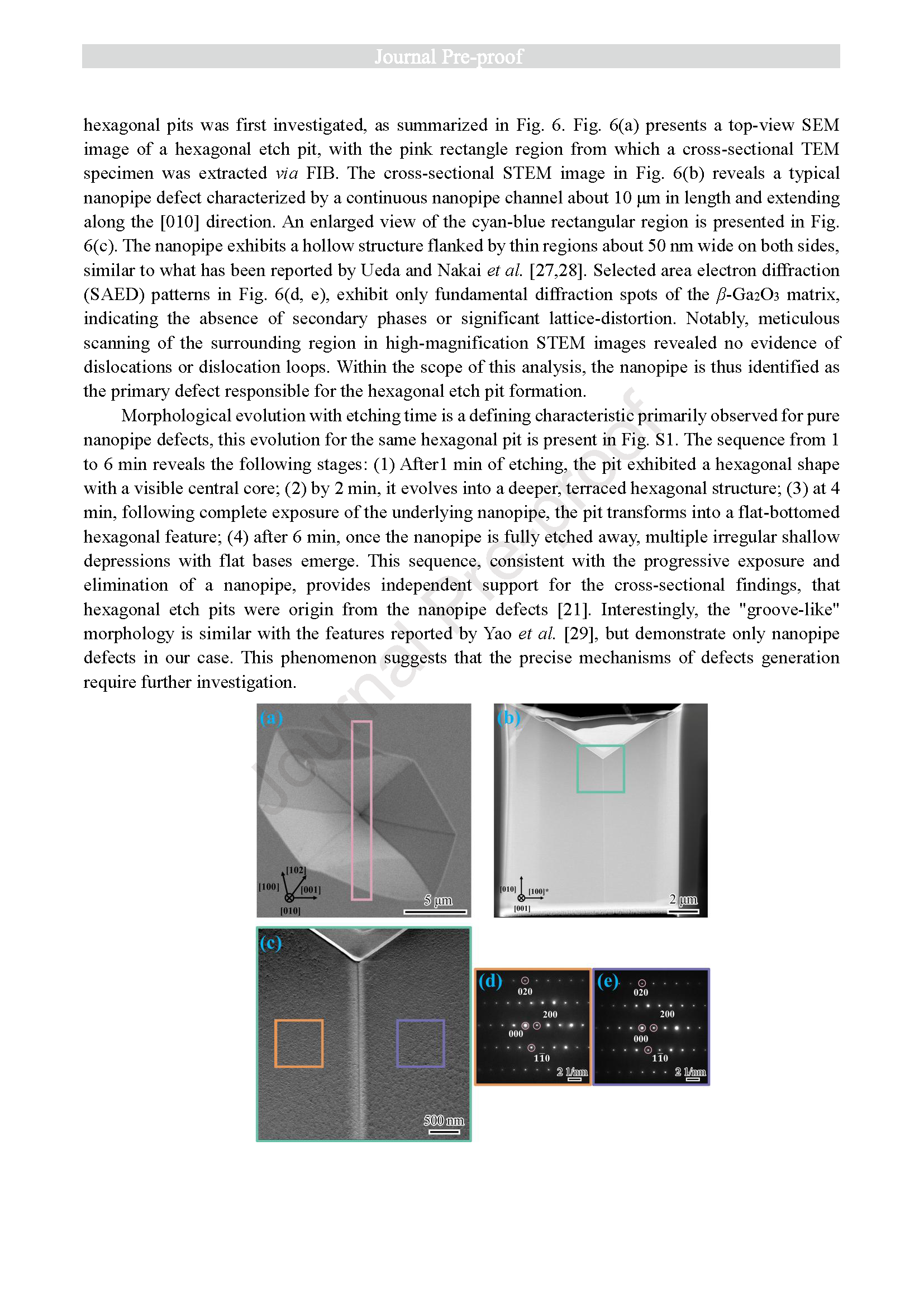
Fig. 6. (a) Plan-view SEM image of the nanopipe-related etch pit and pink solid line square FIB processing schematic diagram. (b) The cross-sectional STEM image of the nanopipe-related etch pit. (c) Magnified STEM image of the nanopipe-related etch pit of the selected cyan solid line square. Selected area electron diffraction (SAED) patterns of (d) the left orange part and (e) the right purple part as labeled in Fig.6(c).
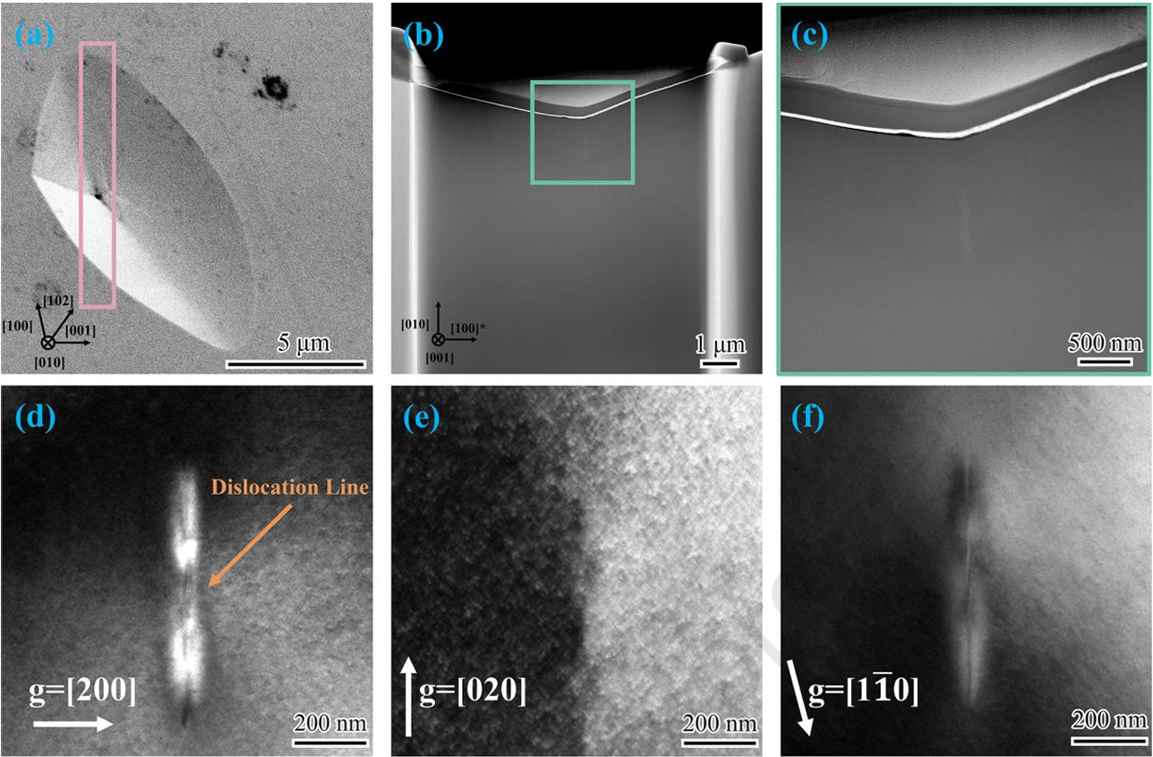
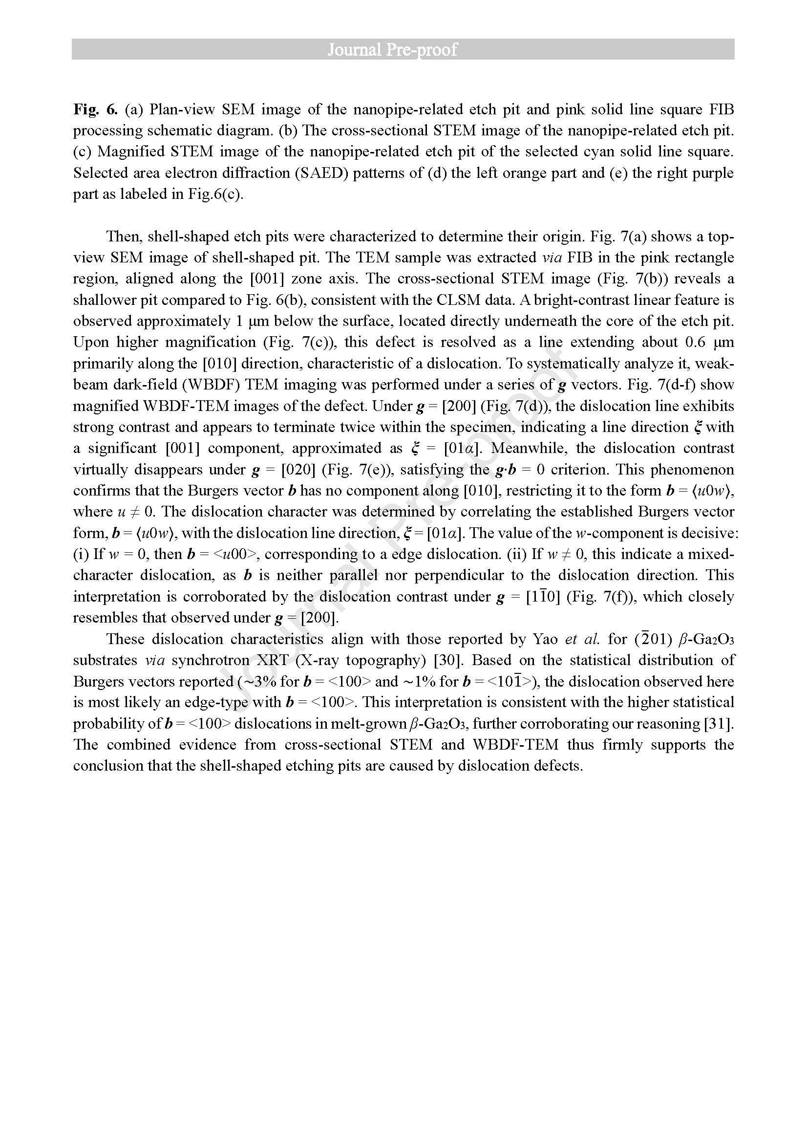
Fig. 7. (a) Plan-view SEM image of the dislocation-type etch pit and the FIB lift-out region (pink square). (b) Cross-sectional STEM image of the dislocation-type etch pit. (c) Magnified STEM image of the dislocation-type etch pit of the selected cyan square region. (d-f) Weak-beam dark field (WBDF) condition TEM images of the dislocation taken at g = [200], g = [020] and g = [11-0], respectively.
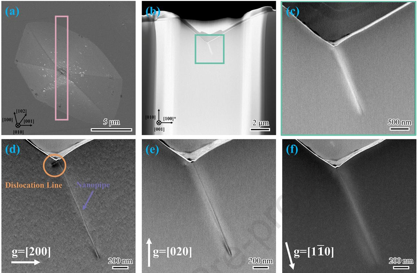
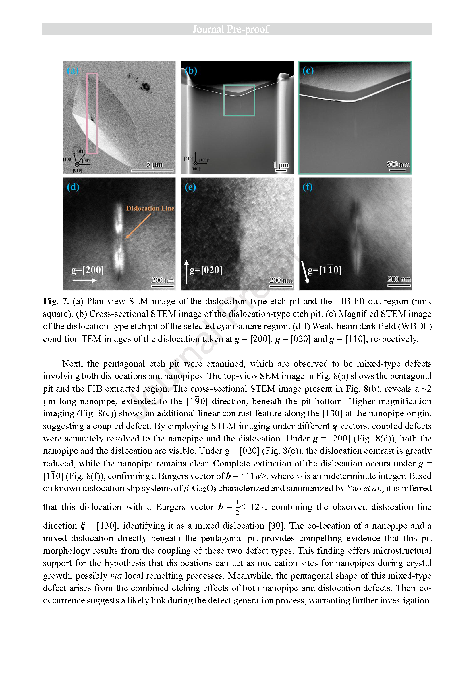
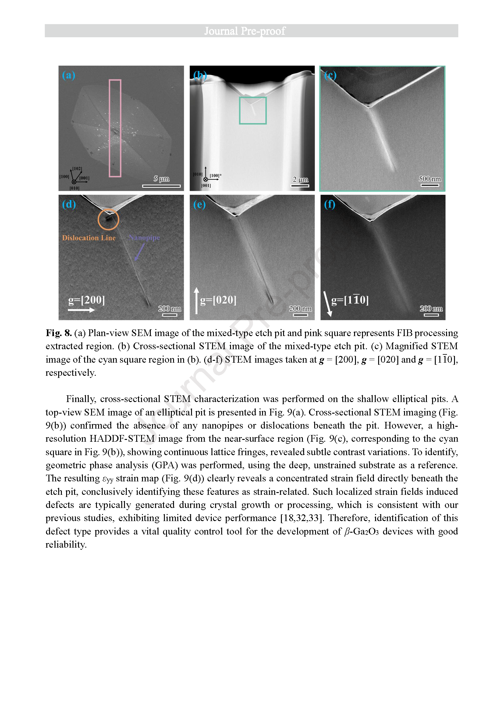
Fig. 8. (a) Plan-view SEM image of the mixed-type etch pit and pink square represents FIB processing extracted region. (b) Cross-sectional STEM image of the mixed-type etch pit. (c) Magnified STEM image of the cyan square region in (b). (d-f) STEM images taken at g = [200], g = [020] and g = [11-0], respectively.
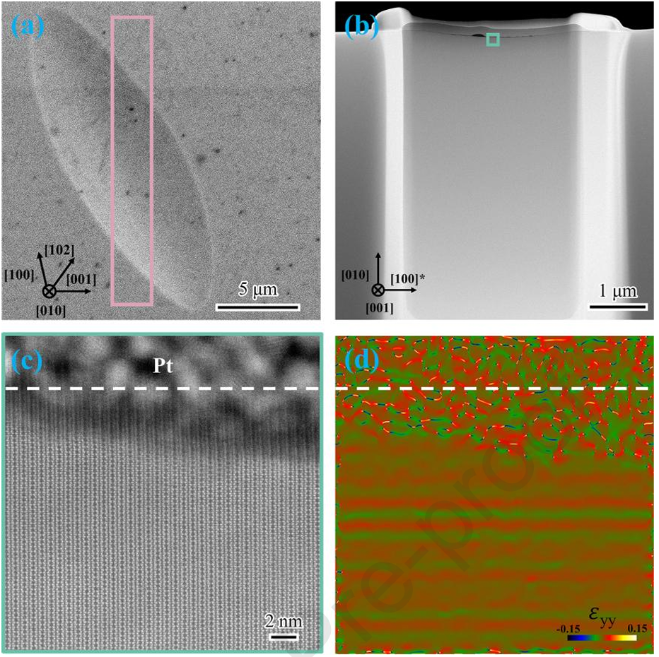
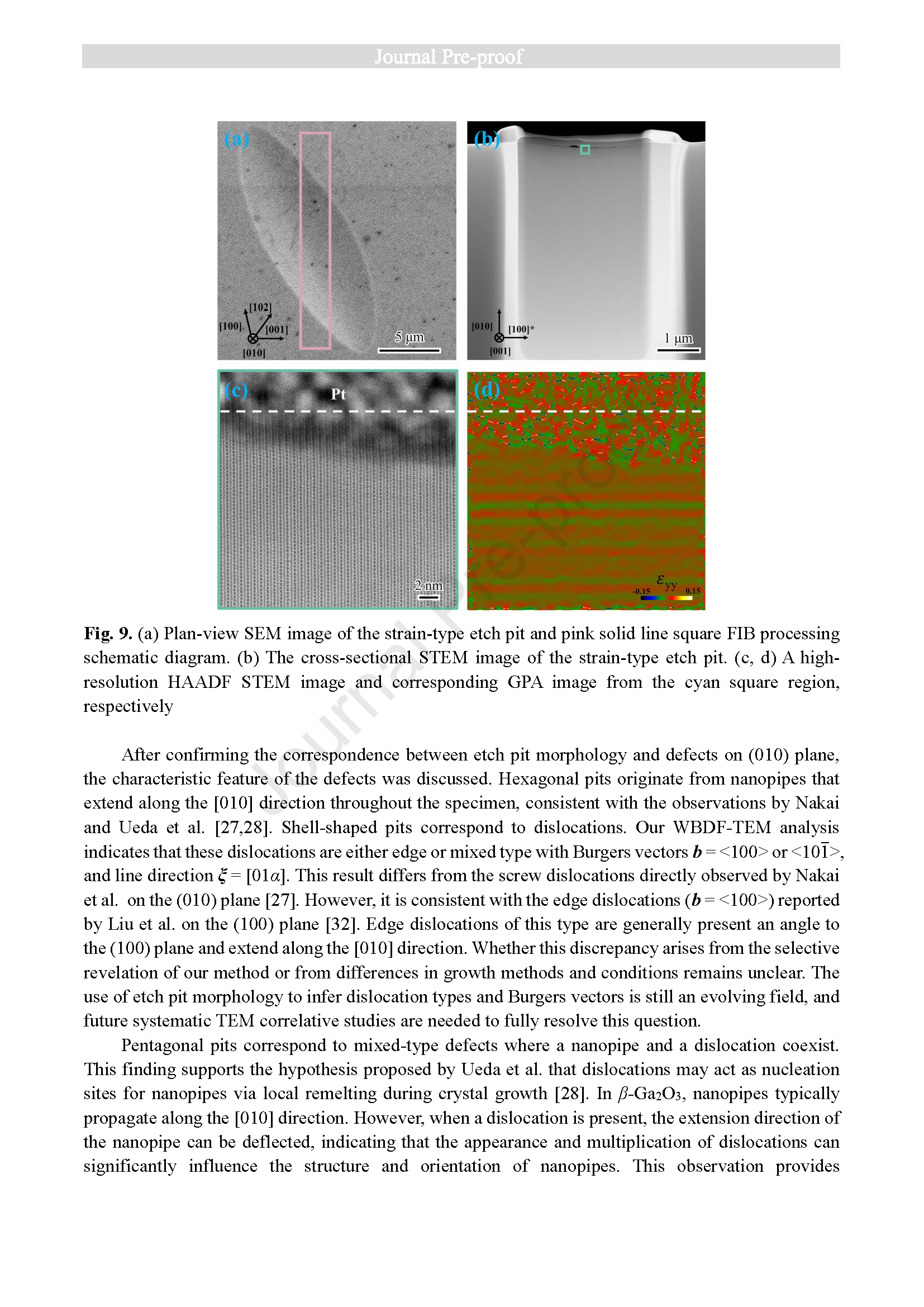
Fig. 9. (a) Plan-view SEM image of the strain-type etch pit and pink solid line square FIB processing schematic diagram. (b) The cross-sectional STEM image of the strain-type etch pit. (c, d) A high resolution HAADF STEM image and corresponding GPA image from the cyan square region, respectively.
DOI:
doi.org/10.1016/j.vacuum.2026.115501