Paper Sharing
【Member Papers】1.75-kV Vertical β-Ga₂O₃ Schottky Barrier Diodes with Room-Temperature Ohmic Contact Formation by a Thin ITO Interlayer
日期:2026-06-04阅读:137
Researchers from the Ningbo Institute of Materials Technology and Engineering have published a dissertation titled " 1.75-kV Vertical β-Ga2O3 Schottky Barrier Diodes with Room-Temperature Ohmic Contact Formation by a Thin ITO Interlayer" in Applied Surface Science.
Background
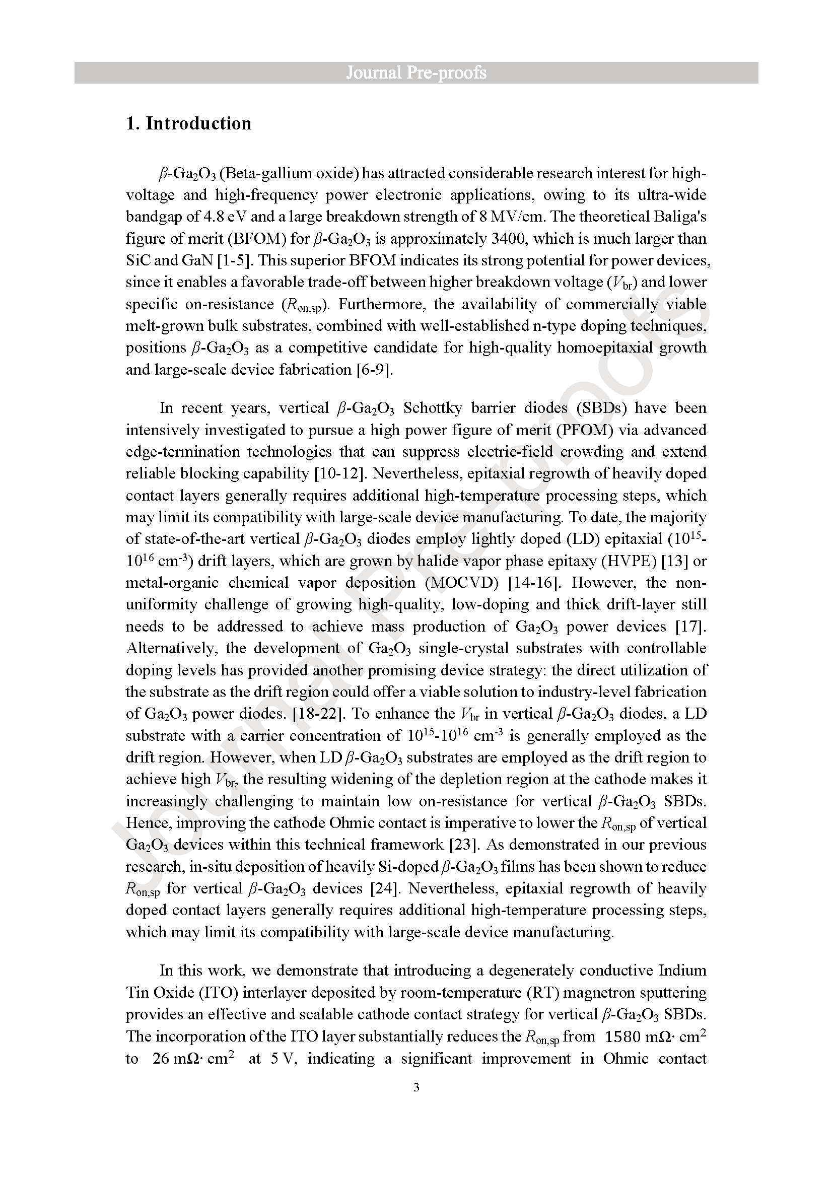
β-Ga2O3 (Beta-gallium oxide) has attracted considerable research interest for high-voltage and high-frequency power electronic applications, owing to its ultra-wide bandgap of 4.8 eV and a large breakdown strength of 8 MV/cm. The theoretical Baliga's figure of merit (BFOM) for β-Ga2O3 is approximately 3400, which is much larger than SiC and GaN. This superior BFOM indicates its strong potential for power devices, since it enables a favorable trade-off between higher breakdown voltage (Vbr) and lower specific on-resistance (Ron,sp). Furthermore, the availability of commercially viable melt-grown bulk substrates, combined with well-established n-type doping techniques, positions β-Ga2O3 as a competitive candidate for high-quality homoepitaxial growth and large-scale device fabrication.
Abstract
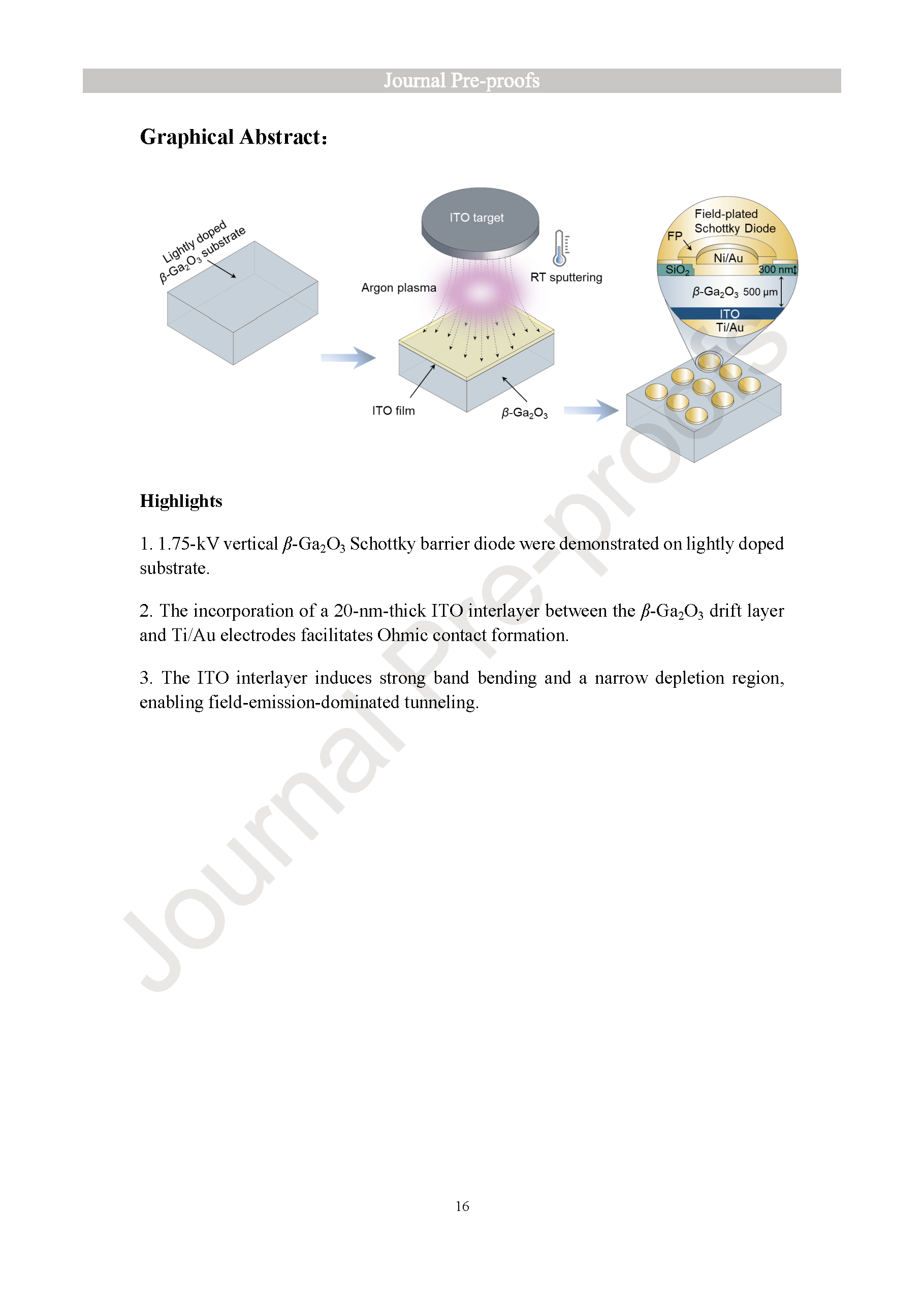
Developing cost-effective Ohmic contacts with ultralow contact resistance and minimal degradation on the drift layer is highly desired for high-performance β-Ga₂O₃ power devices. In this letter, we demonstrate a 1.75-kV vertical Schottky barrier diode (SBD) based on a lightly doped β-Ga2O3 single-crystal substrate with Ohmic contacts sputtered at room temperature. The construction of β-Ga2O3 SBDs with a SiO2 field-plate structure achieves a Schottky barrier height of 0.93 eV and a breakdown voltage of 1.75 kV, but suffers from large contact resistance on the cathode side with a direct Ti/Au bilayer electrode. The incorporation of a 20-nm-thick ITO interlayer between the β-Ga2O3 drift layer and Ti/Au electrodes facilitates Ohmic contact formation that exhibits a specific contact resistivity of 2.6 ×10⁻⁵ Ω·cm2 and an ideality factor of 1.10. This substantially reduces the specific on-resistance (Ron,sp) of the β-Ga2O3 SBDs by nearly two orders of magnitude from 1580 mΩ·cm² to 26 mΩ·cm². The use of a thin and degenerately doped ITO interlayer is critical to induce abrupt band bending and construct a narrow depletion region for field-emission-dominated tunneling, thus forming a more ideal Ohmic contact. The room-temperature Ohmic contact strategy is expected to facilitate industry-level device application of β-Ga2O3 power devices.
Highlights
A low-resistance Ohmic contact is realized on lightly doped β-Ga2O3 substrate by room-temperature sputtered ITO interlayer.
The 20 nm ITO interlayer reduces the specific on-resistance by nearly two orders of magnitude while maintaining a high breakdown voltage of 1.75 kV.
The ITO interlayer enables efficient field-emission-dominated carrier tunneling by inducing abrupt band bending and narrow depletion region.
Conclusion
We have demonstrated a 1.75-kV vertical β-Ga2O3 substrate-based Schottky barrier diode with low Ohmic contact resistivity enabled by introducing a 20-nm degenerately doped ITO interlayer sputtered at room temperature. The thin and degenerately doped ITO interlayer induces strong band bending and a narrow depletion region, enabling field-emission-dominated tunneling and more efficient carrier transport. This approach effectively overcomes the large contact resistance with lightly doped β-Ga2O3 and Ti/Au, leading to a low Ohmic contact resistivity of 2.6 ×10⁻⁵ Ω·cm² at the cathode. The Ron,sp of the vertical β-Ga2O3 SBD with 20-nm ITO interlayer is substantially reduced by nearly two orders of magnitude from 1580 mΩ·cm² to 26 mΩ·cm², while a Schottky barrier height of 0.93 eV is simultaneously maintained. This room-temperature Ohmic contact strategy provides a practical and scalable route toward high-performance and industry-relevant β-Ga2O3 power device applications.
Project Support
This work was supported by the National Natural Science Foundation of China (Grant No. 62204244) and the Zhejiang Provincial Natural Science Foundation of China (Grant No. LQ23F040003). Part of the research was supported by Ningbo Yongjiang Talent Introduction Programme (Grant No. 2021A-046-C).
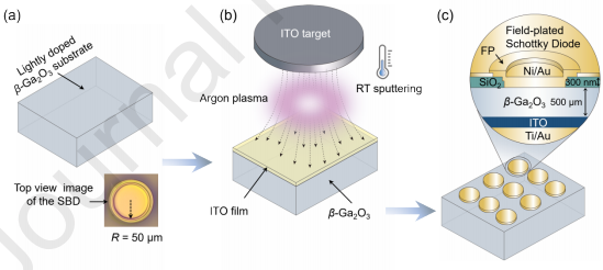
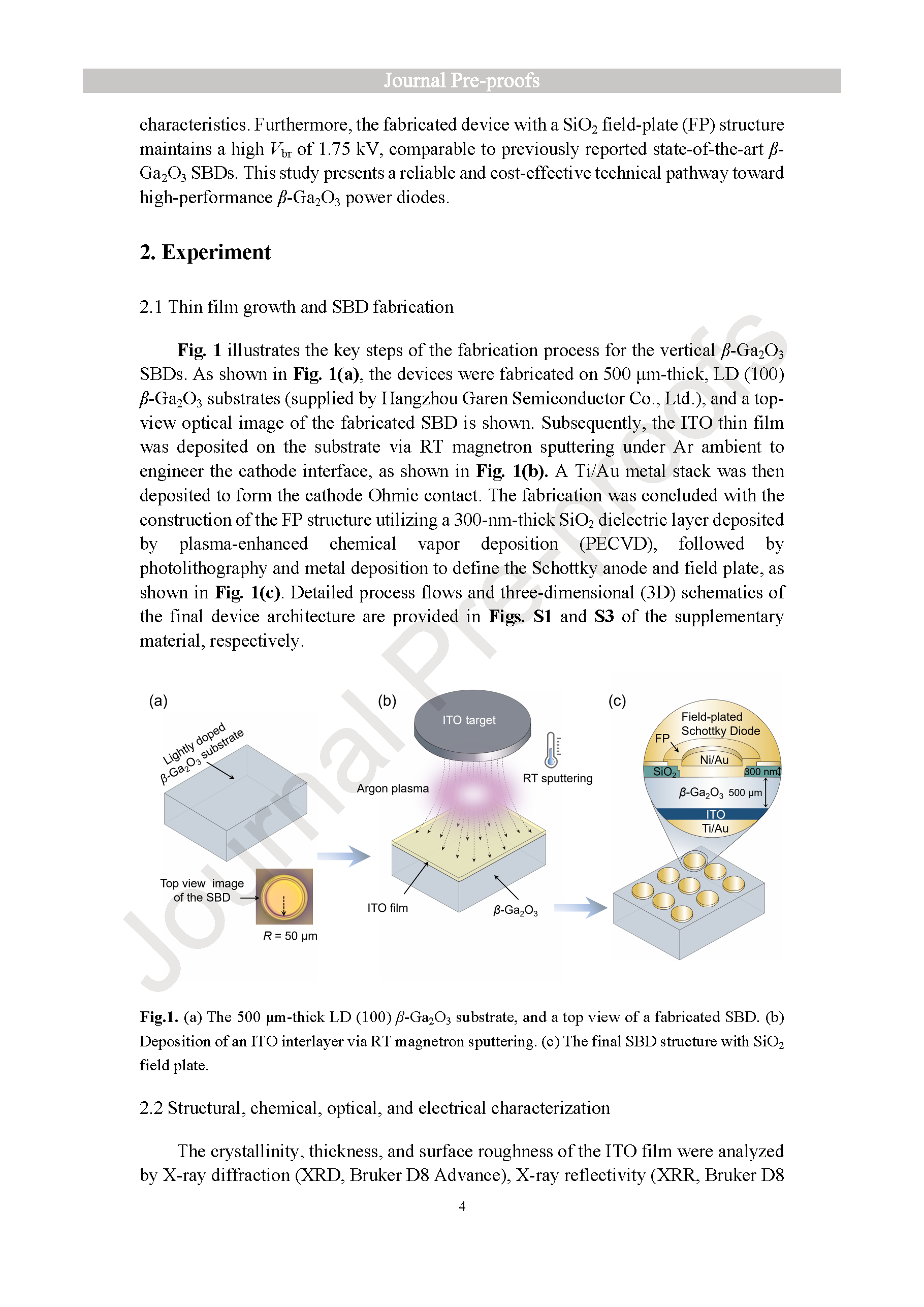
图1. (a) 500 μm 厚轻掺杂 (100) 晶向 β-Ga2O3 衬底及制备完成的肖特基二极管顶视图;(b) 室温磁控溅射沉积 ITO 中间层;(c) 带有 SiO2 场板的最终二极管结构。
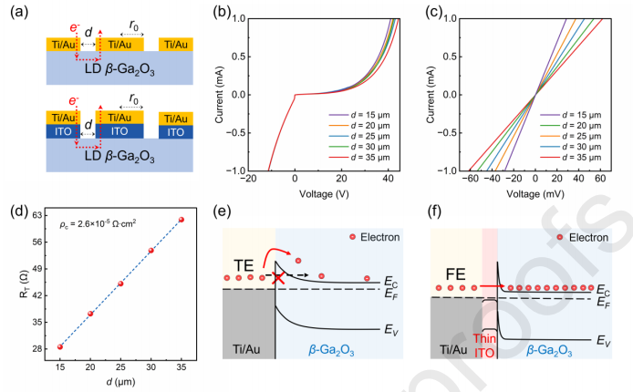
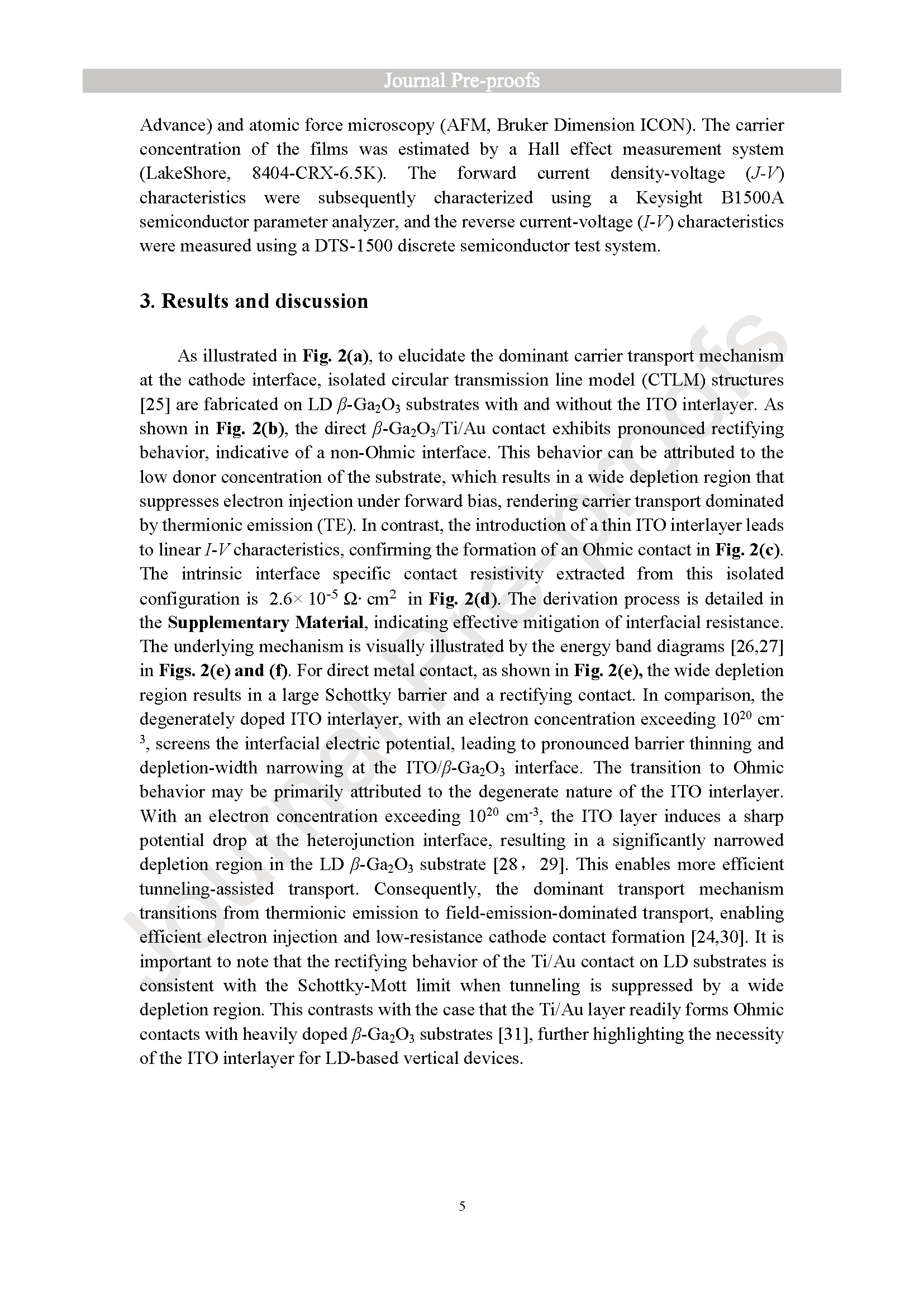
图2. (a) Ti/Au 与轻掺杂 β-Ga2O3 直接接触(上)、ITO 中间层接触(下)的独立圆形传输线模型(CTLM)截面示意图;(b) β-Ga2O3/Ti/Au 直接接触的 I-V 特性;(c) β-Ga2O3/ITO/Ti/Au 接触的欧姆特性 I-V 曲线;(d) 20 nm ITO 中间层的 β-Ga₂O₃/ITO/Ti/Au 接触比接触电阻率提取;(e) 以热电子发射(TE)为主的 β-Ga2O3/Ti/Au 接触载流子输运机制与能带示意图;(f) 以场发射(FE)为主的 β-Ga2O3/ITO/Ti/Au 接触载流子输运机制与能带示意图。
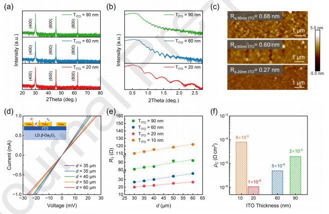
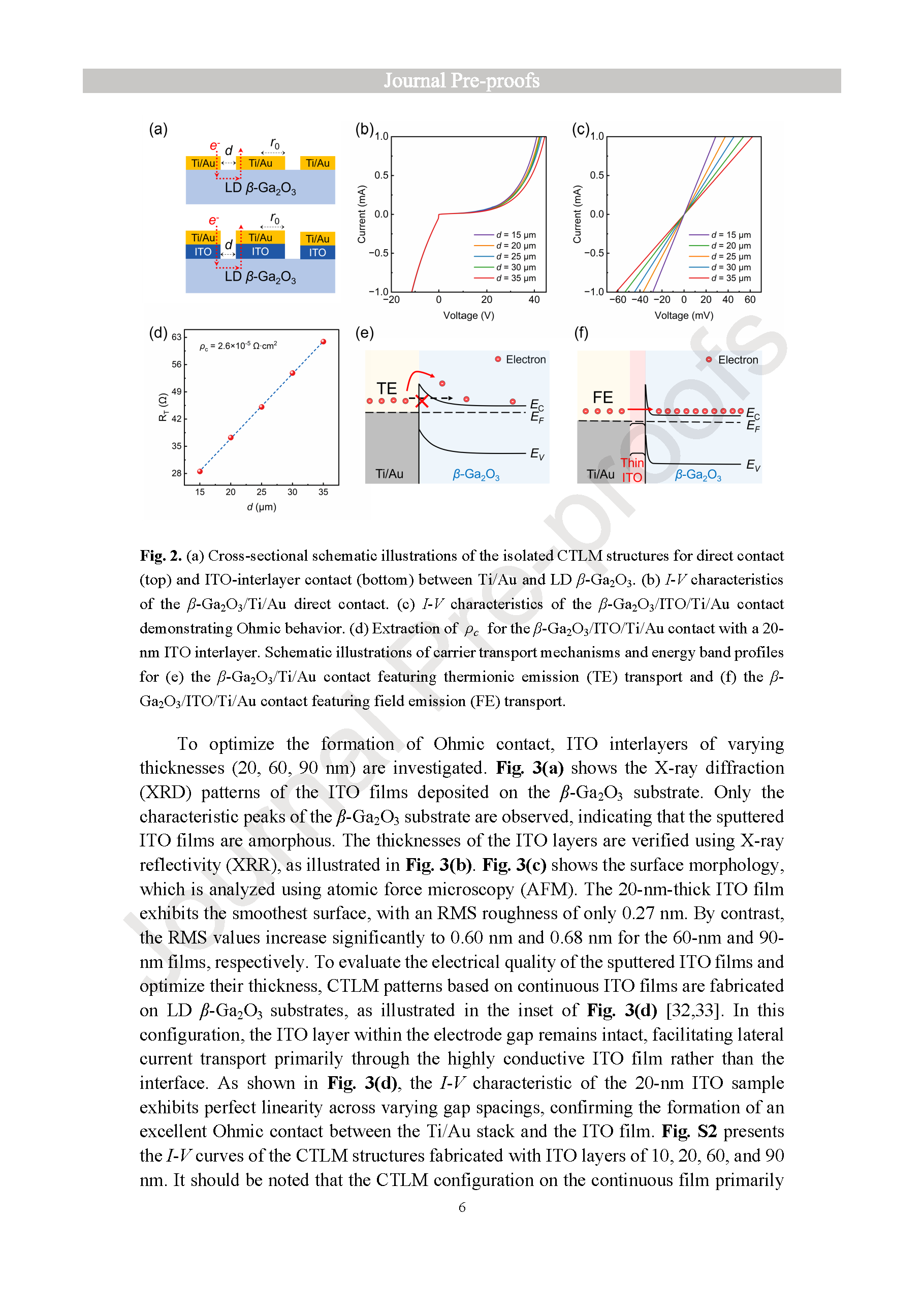
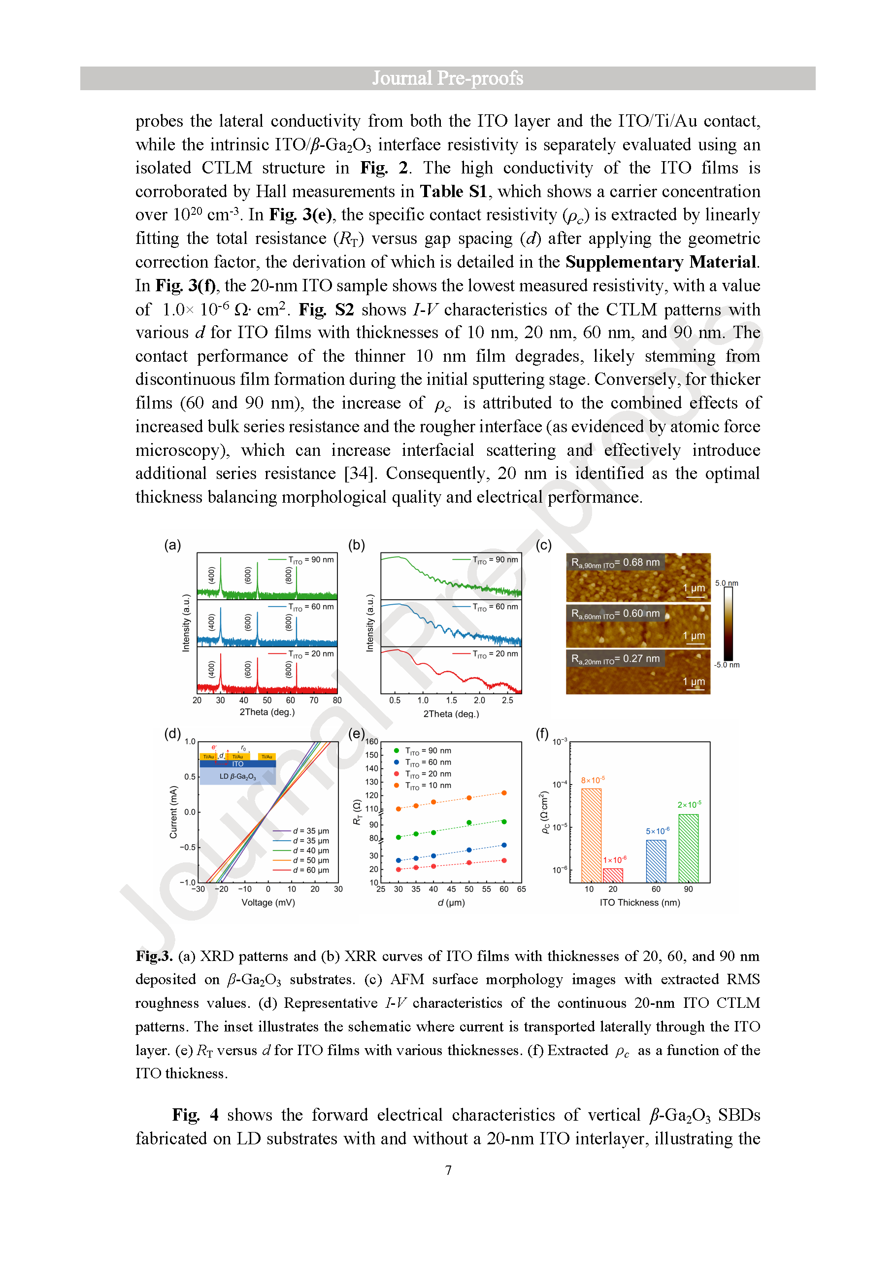
图3. (a) 沉积在 β-Ga2O3 衬底上 20、60、90 nm 厚 ITO 薄膜的 XRD 图谱;(b) 对应 XRR 曲线;(c) AFM 表面形貌图及均方根粗糙度;(d) 连续 20 nm ITO 的 CTLM 结构典型 I-V 特性,插图为电流经 ITO 层横向输运示意图;(e) 不同厚度 ITO 的总电阻 RT 与电极间距 d 关系;(f) 提取的比接触电阻率随 ITO 厚度变化曲线。
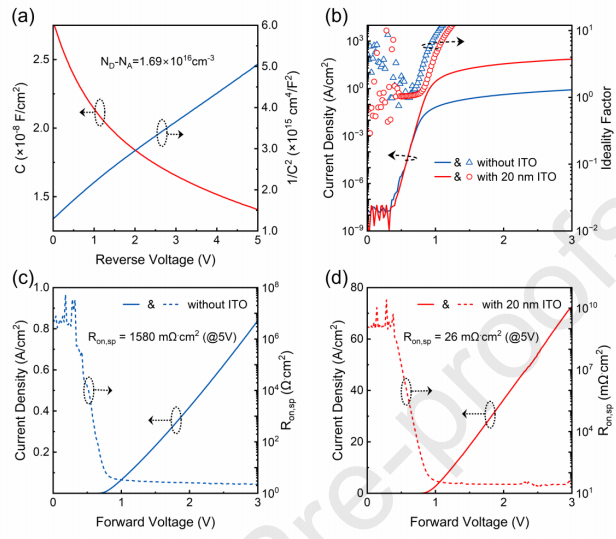
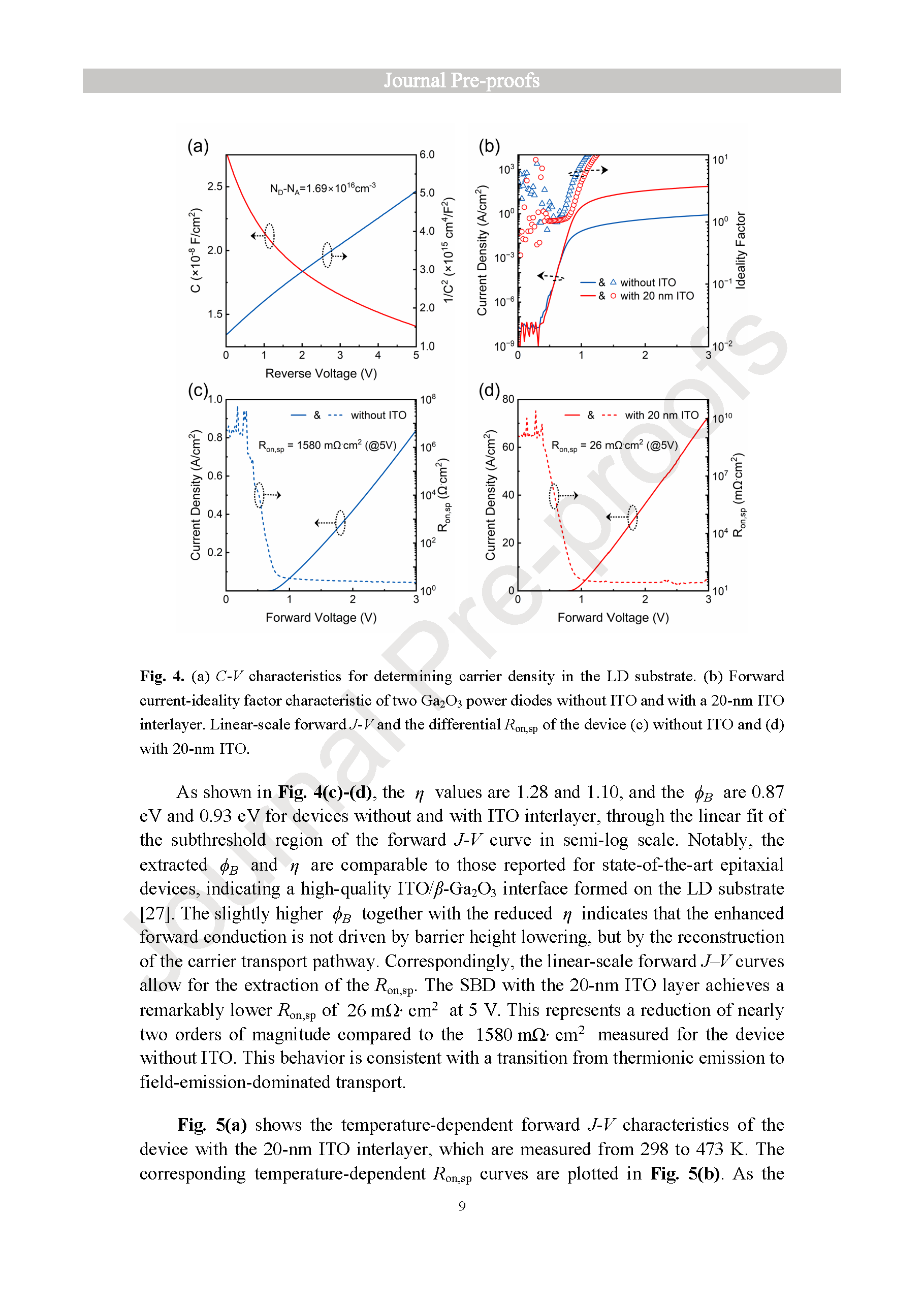
图4. (a) 用于确定轻掺杂衬底载流子浓度的 C-V 特性;(b) 无 ITO 与 20 nm ITO 中间层的两种氧化镓功率二极管正向电流 - 理想因子特性;(c) 无 ITO 器件的线性尺度正向 J-V 与微分比导通电阻;(d) 20 nm ITO 器件的线性尺度正向 J-V 与微分比导通电阻。
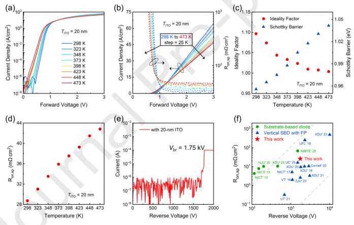
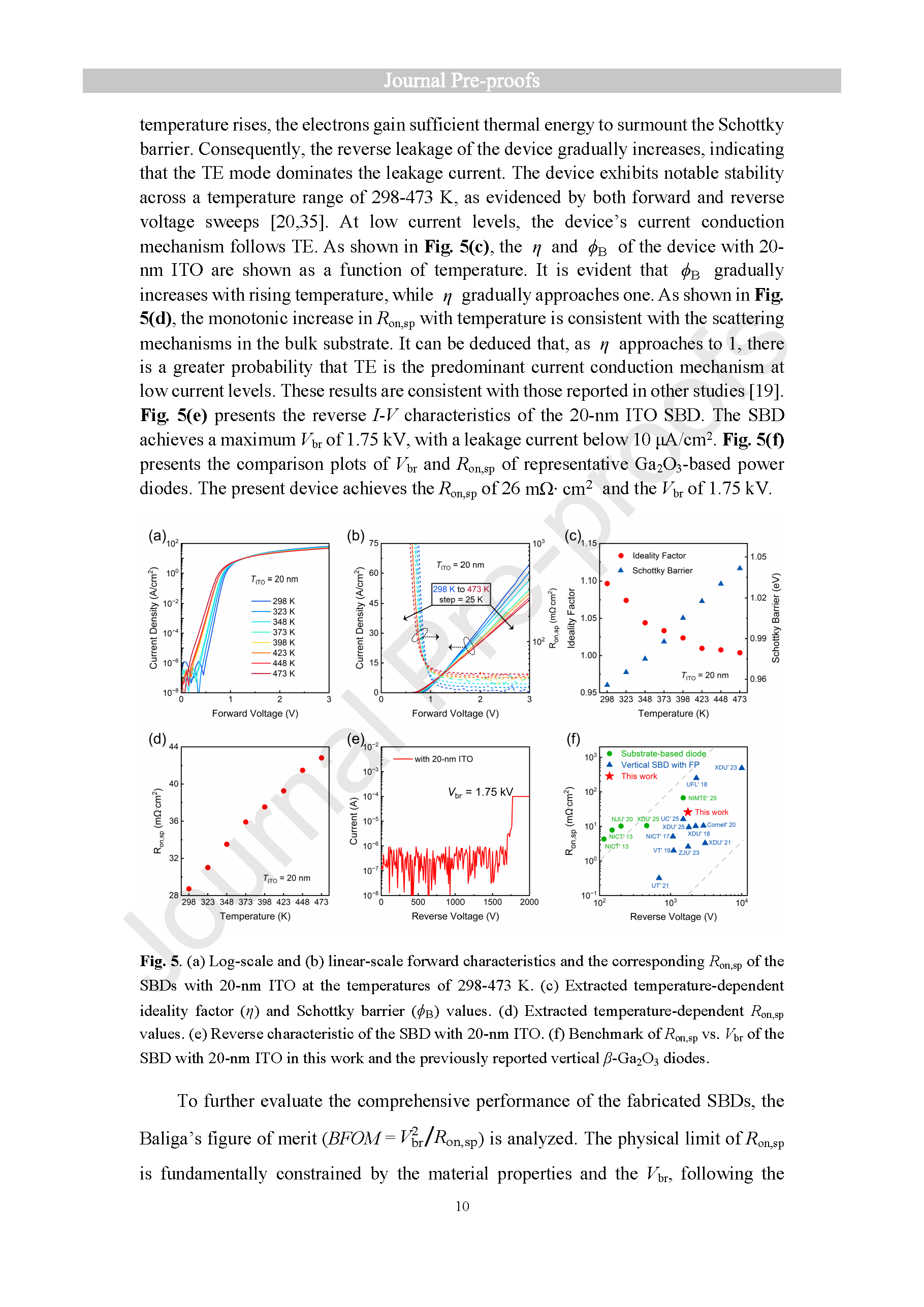
图5. (a) 298–473 K 下含 20 nm ITO 肖特基二极管的对数尺度正向特性;(b) 线性尺度正向特性及对应比导通电阻;(c) 提取的随温度变化的理想因子与肖特基势垒高度;(d) 提取的随温度变化的比导通电阻;(e) 含 20 nm ITO 二极管的反向特性;(f) 本文器件与已报道垂直 β-Ga2O3 二极管的比导通电阻 - 击穿电压性能对比。
DOI:
doi.org/10.1016/j.apsusc.2026.167007