Paper Sharing
【Domestic Papers】High-performance self-powered p‑GaN/Ga₂O₃ solar-blind photodetector via in situ GaON interface engineering
日期:2026-06-05阅读:116
Researchers from the Sun Yat-Sen University have published a dissertation titled " High-performance self-powered p-GaN/Ga2O3 solar-blind photodetector via in situ GaON interface engineering " in Journal of Physics D: Applied Physics.
Background
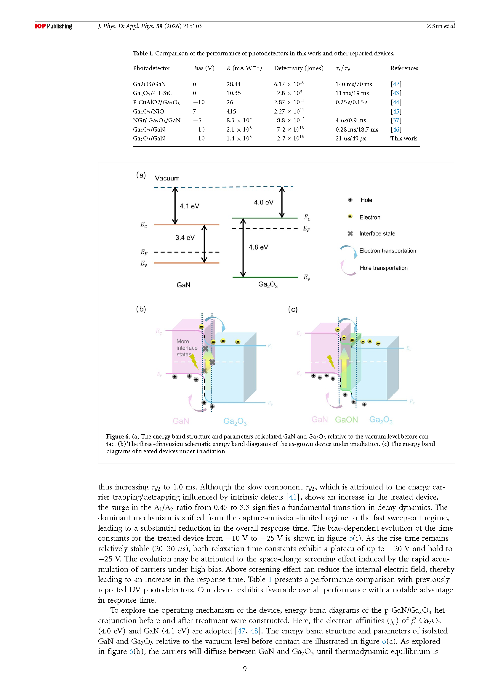
Solar-blind deep ultraviolet (DUV) photodetectors have irreplaceable strategic value in missile warning, secure communication, environmental monitoring, ozone analysis and other fields. Wide-bandgap semiconductors are the core materials for preparing such detectors, and ZnMgO, AlGaN, diamond, BN, Ga₂O₃ and other systems are commonly used candidates. Among them, AlGaN and MgZnO require high component doping, which easily leads to lattice mismatch, high dislocation density, phase separation and other problems; although diamond and BN have suitable band gaps for solar-blind band, their high fabrication cost, stringent process requirements and difficulty in obtaining large-size high-quality single crystal substrates limit commercial applications. β‑Ga₂O₃ has an intrinsic band gap of about 4.9 eV, which naturally matches the 200–280 nm solar-blind spectrum without complex alloying. It also has excellent theoretical breakdown field and figure of merit, and can prepare large-size high-quality single crystal substrates by low-cost melt methods, making it an ideal solar-blind detection material. However, efficient p-type doping of Ga₂O₃ is difficult to achieve, so constructing heterojunctions has become a mainstream solution, and p‑GaN is the preferred partner due to lattice matching and mature doping technology. p‑GaN/n‑Ga₂O₃ heterojunction has type‑II band alignment, with small conduction band offset facilitating electron transport and large valence band offset blocking electron back-injection, strong built-in electric field and high carrier separation efficiency. Nevertheless, the heterointerface of Ga₂O₃ suffers from interface states caused by lattice mismatch and high surface dangling bond density, resulting in high dark current, slow response speed, and difficulty in balancing gain and speed. Interface passivation engineering has become a key method to optimize device performance.
Abstract
Semiconductor interface engineering is critical for optimizing heterojunction optoelectronic devices. In this paper, we report on a high-performance self-powered p‑GaN/Ga₂O₃ heterojunction solar-blind photodetector enhanced via an in situ–generated GaON interlayer. Using oxygen plasma treatment and high-temperature annealing, the GaON layer acts as a modulation spacer that physically separates the heterojunction interface. The artificially designed interlayer can effectively extend the depletion region and suppresses band-to-band tunneling, leading to a dramatic reduction in dark current. The treated detector exhibits a dark current reduction of 4 orders of magnitude (down to 10 pA at −10 V), enabling highly specific detectivity of 2.7×10¹³(1.6×10¹³) Jones at 250 nm (350 nm) and achieves a remarkable responsivity of 1.4 (0.75) A W⁻¹ at 250 nm (350 nm). In addition, the optimized device structure enables a fast separation of electron-hole pairs, yielding rapid rise/decay times of 21 µs/49 µs. Our findings demonstrate the remarkable role of GaON interlayers in suppressing the leakage current and modulating carrier dynamics, offering an effective route for fabricating high-sensitivity, self-powered semiconductor UV photon detectors.
Highlights
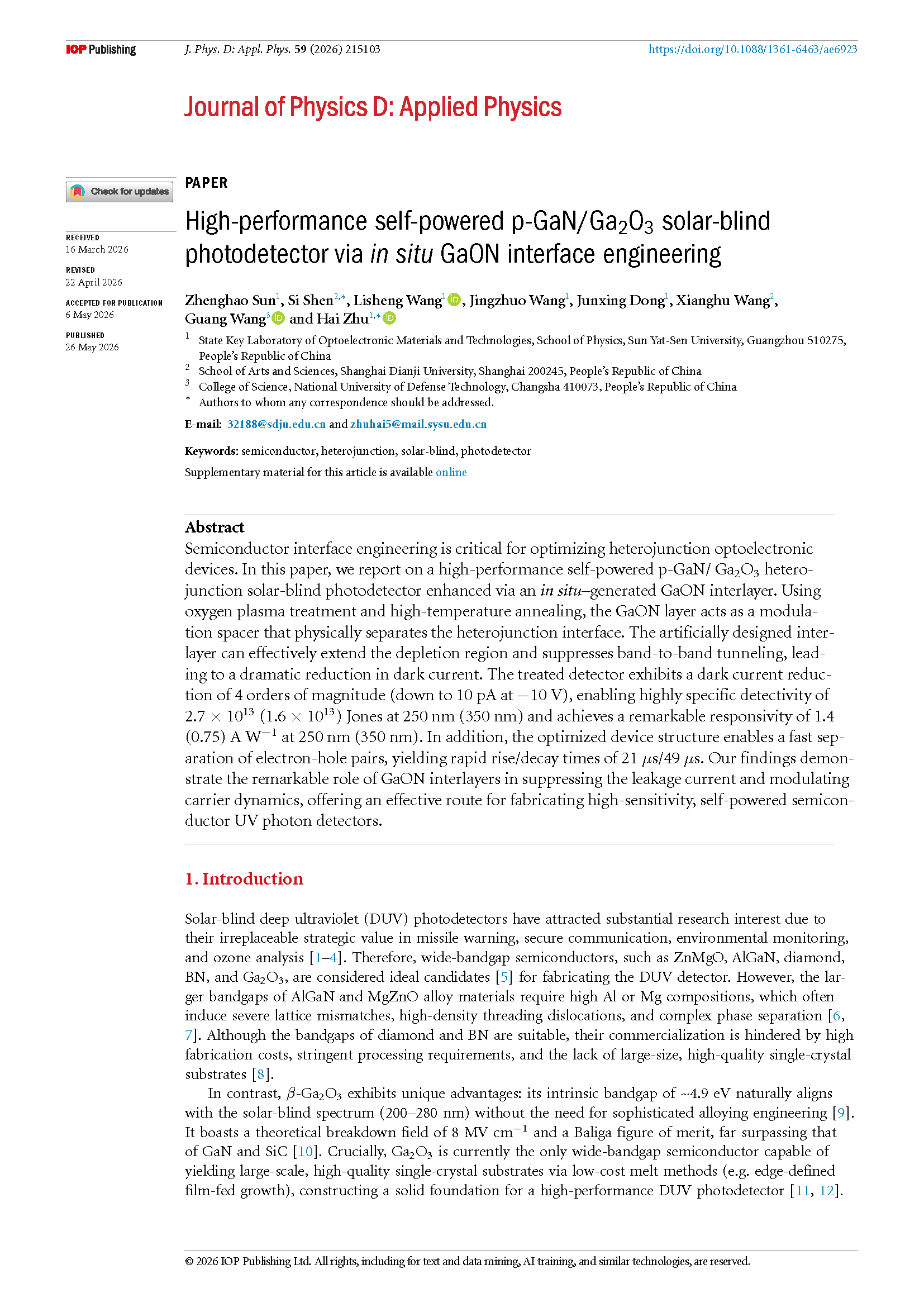
A GaON interlayer is in-situ fabricated on p‑GaN surface by two-step process of oxygen plasma treatment and high-temperature annealing, realizing precise modulation of heterojunction interface.
GaON layer acts as both buffer layer and passivation layer, alleviating lattice mismatch and passivating interface states, reducing dark current by 4 orders of magnitude.
Stepped type‑II band alignment is constructed to balance gain and response speed, realizing self-powered, high responsivity, high detectivity and ultra-fast response solar-blind detection.
The device achieves specific detectivity of 2.7×10¹³ Jones at −10 V, with rise/decay time of 21 μs/49 μs, showing better comprehensive performance than most reported Ga₂O₃-based UV photodetectors.
Conclusion
In summary, we successfully constructed a p‑GaN/Ga₂O₃ heterojunction DUV photodetector based on an in situ GaON interlayer on a p‑GaN surface via a two-step fabrication process via oxygen plasma treatment and 900 ℃ nitrogen annealing. Raman spectroscopy and XPS characterization confirmed the formation of the GaON layer. The treated p‑GaN/Ga₂O₃ detector exhibits excellent performance and the photon-excited electron-hole pairs can be efficiently separated through a built-in electric field under zero bias, thereby enabling self-powered operation. The photodetector demonstrates a high light-to-dark ratio with an ultra-low dark current of 10 pA, high responsivities of 1.4 A W⁻¹ under 250 nm and 0.75 A W⁻¹ under 350 nm. Furthermore, a scheme for fast transient response speeds with rise/decay times of 21 µs/49 µs is explored using the p‑GaN/Ga₂O₃ heterojunction energy band. Our work provides valuable insights for the development of high-performance Ga₂O₃-based self-powered UV photodetectors for various practical applications.
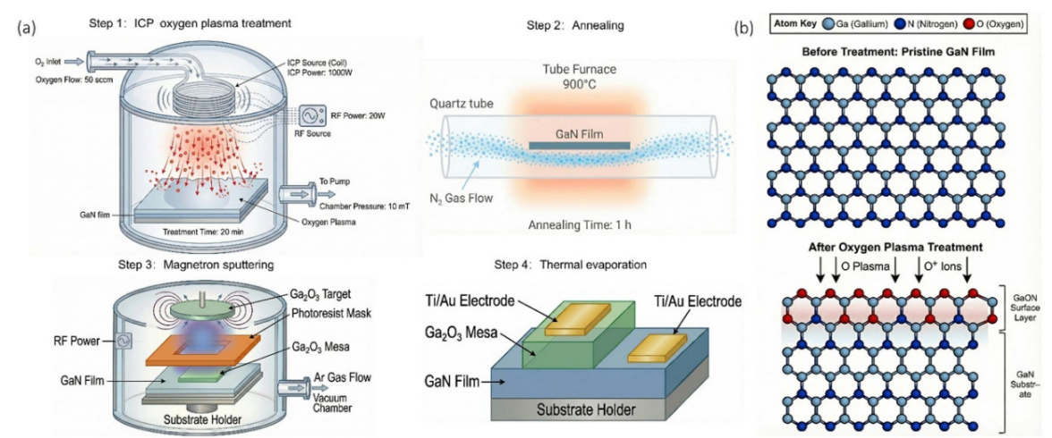
Figure 1. (a) The fabrication process of the GaN/Ga₂O₃ heterojunction photodetector. (b) Schematic diagrams of the atomic structure of the GaN surface before (top) and after (bottom) the oxygen plasma treatment.
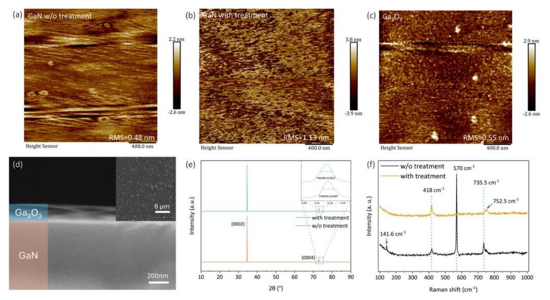
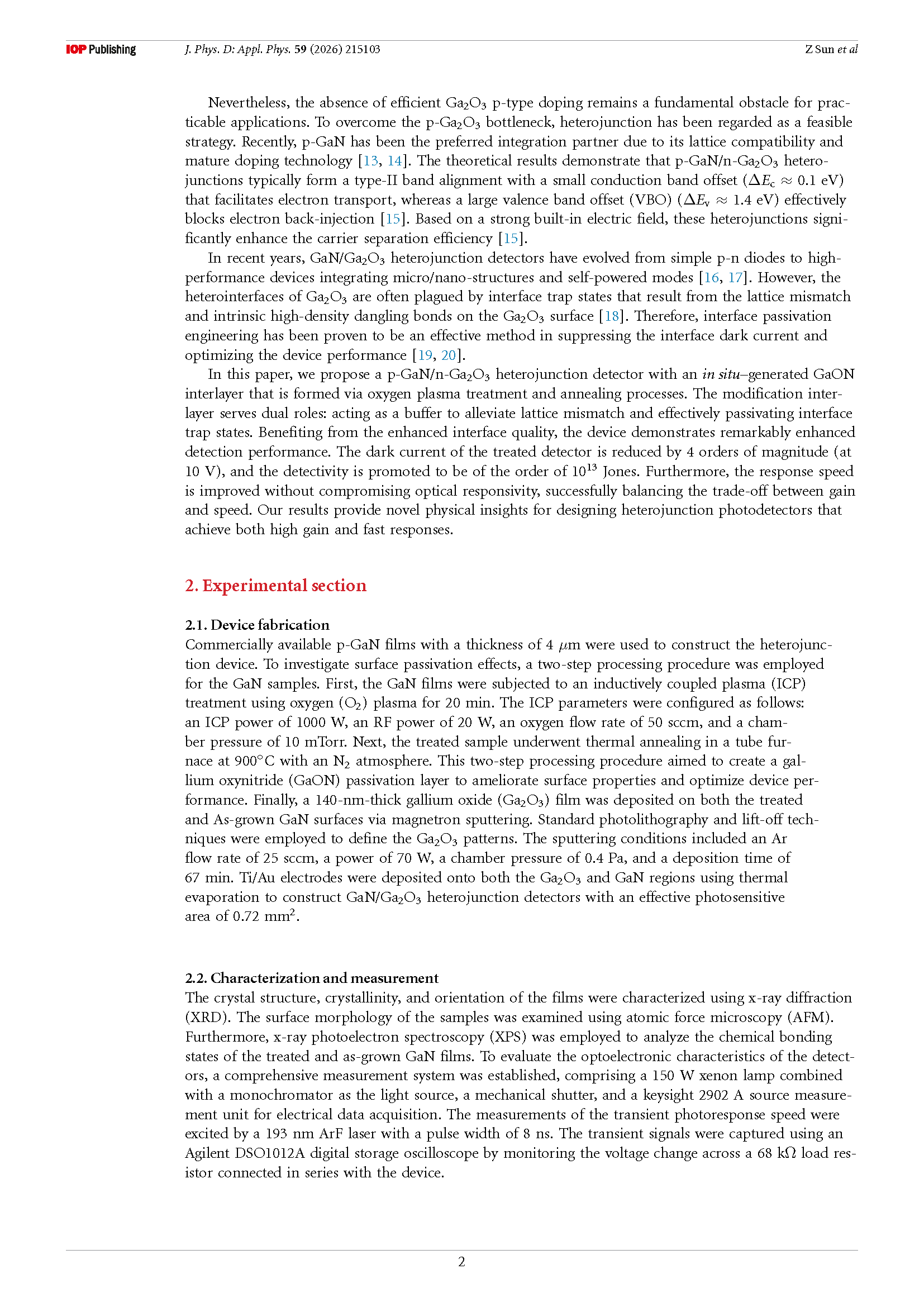
Figure 2. (a) Atomic force microscopy (AFM) image shows the surface morphology of the pristine GaN film without treatment. (b) The image of GaN film following oxygen plasma treatment. (c) The image of the deposited Ga₂O₃ film. (d) Cross-sectional scanning electron microscopy image of the Ga₂O₃/GaN heterojunction, with the inset depicting the surface of treated GaN film. (e) The x-ray diffraction (XRD) patterns of the GaN films before and after treatment, with the inset displaying a magnified view of the (0004) diffraction peak. (f) Raman spectra of the GaN films with and without treatment.
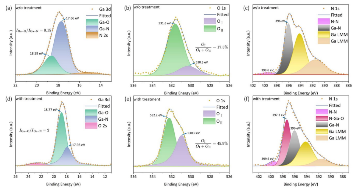
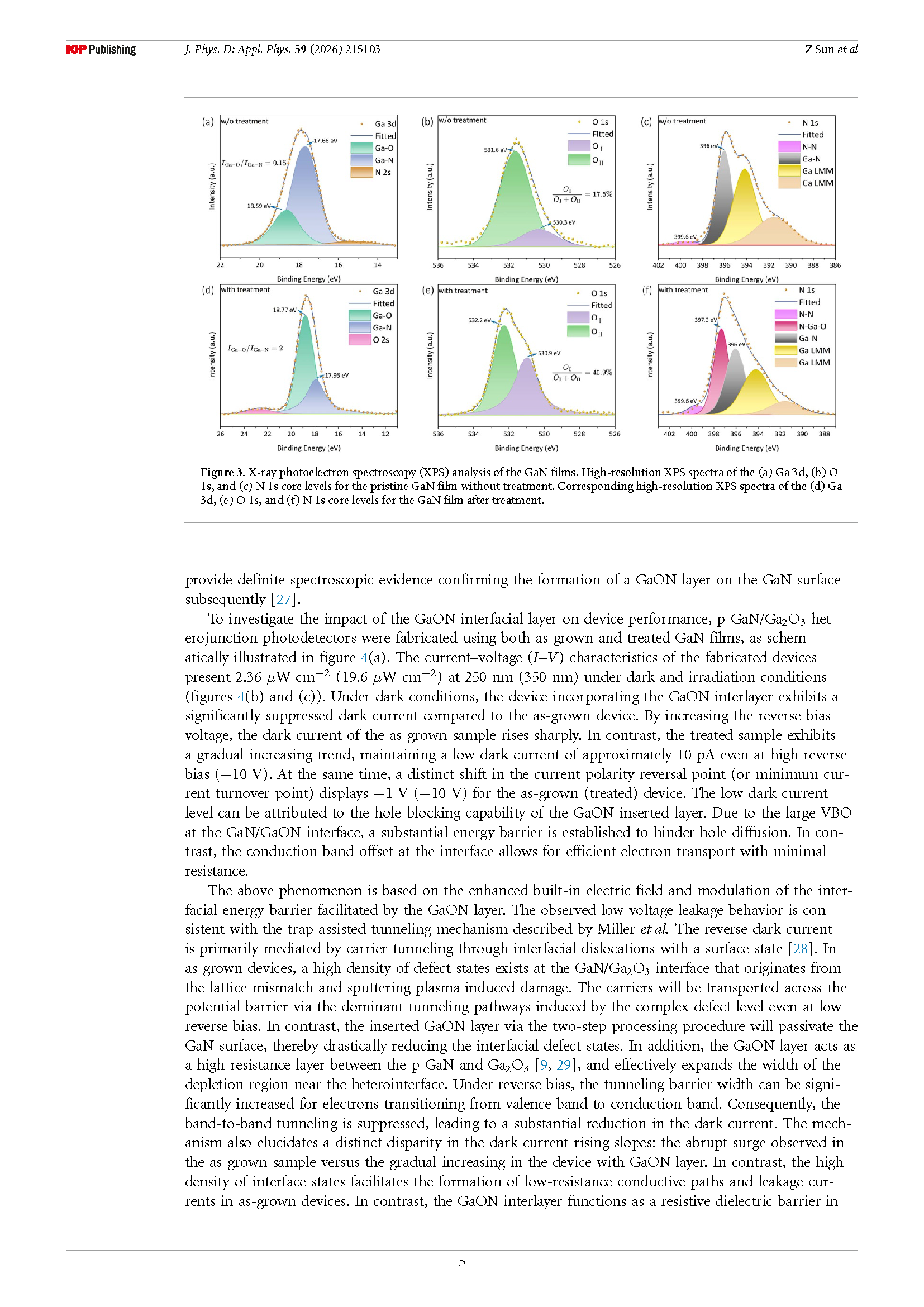
Figure 3. X-ray photoelectron spectroscopy (XPS) analysis of the GaN films. High-resolution XPS spectra of the (a) Ga 3d, (b) O 1s, and (c) N 1s core levels for the pristine GaN film without treatment. Corresponding high-resolution XPS spectra of the (d) Ga 3d, (e) O 1s, and (f) N 1s core levels for the GaN film after treatment.
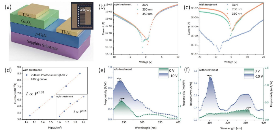
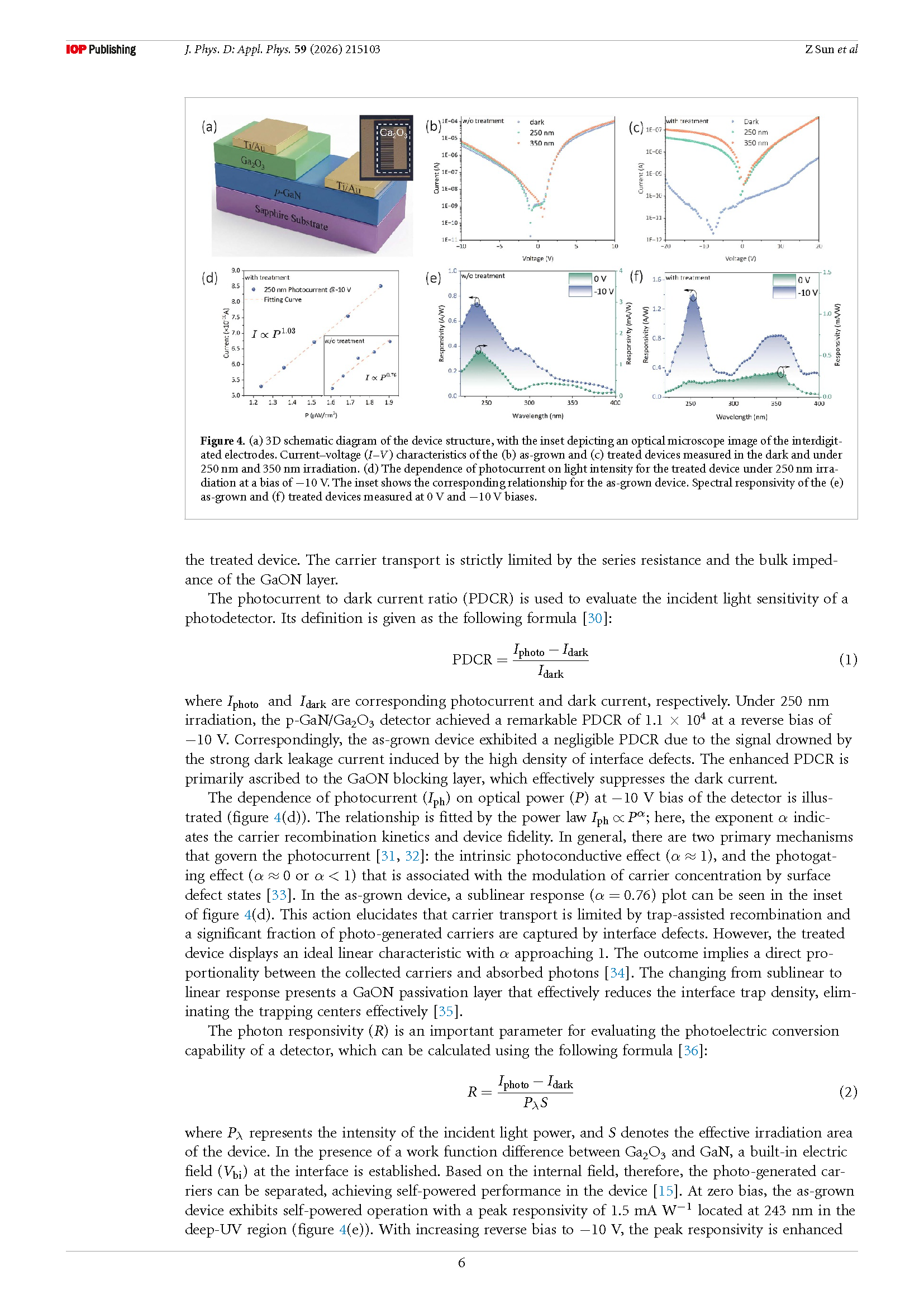
Figure 4. (a) 3D schematic diagram of the device structure, with the inset depicting an optical microscope image of the interdigitated electrodes. Current–voltage (I–V) characteristics of the (b) as-grown and (c) treated devices measured in the dark and under 250 nm and 350 nm irradiation. (d) The dependence of photocurrent on light intensity for the treated device under 250 nm irradiation at a bias of −10 V. The inset shows the corresponding relationship for the as-grown device. Spectral responsivity of the (e) as-grown and (f) treated devices measured at 0 V and −10 V biases.
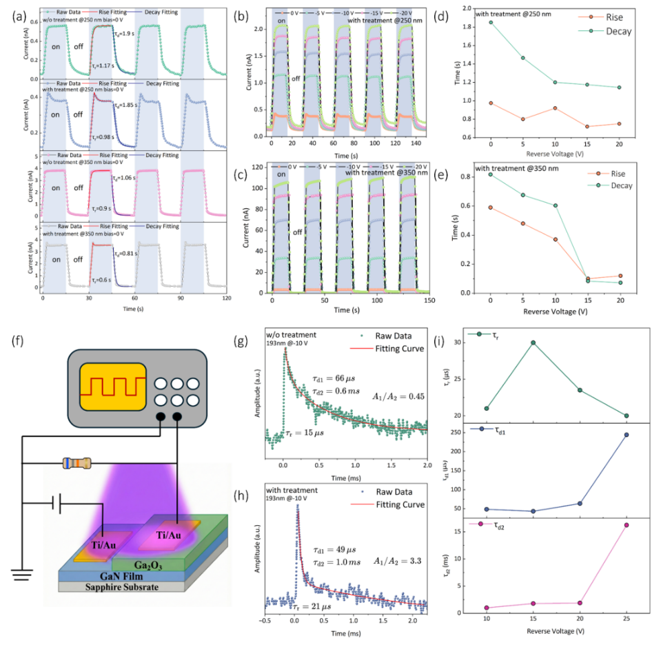
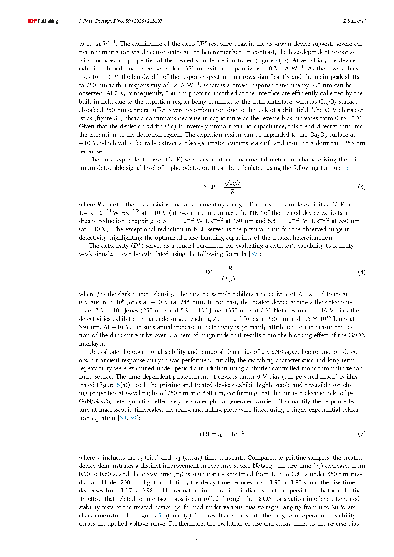
Figure 5. (a) Time-dependent photoresponse (I–t) curves and corresponding exponential fits for the as-grown and treated devices under 250 nm and 350 nm irradiation at 0 V bias. I–t characteristics of the treated device under various reverse biases from 0 V to −20 V under (b) 250 nm and (c) 350 nm irradiation. Extracted rise and decay times as a function of reverse bias for the treated device under (d) 250 nm and (e) 350 nm irradiation. (f) Schematic diagram of the high-speed transient response measurement setup using a pulsed laser. High-speed transient response curves and bi-exponential decay fits for the (g) as-grown and (h) treated devices measured under 193 nm pulsed laser excitation at a bias of −10 V. (i) Extracted transient time constants (τr, τd1, τd2) as a function of reverse voltage under 193 nm pulsed excitation.
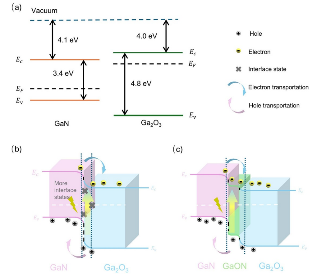
Figure 6. (a) The energy band structure and parameters of isolated GaN and Ga₂O₃ relative to the vacuum level before contact.(b) The three-dimension schematic energy band diagrams of the as-grown device under irradiation. (c) The energy band diagrams of treated devices under irradiation.
DOI :
10.1088/1361-6463/ae6923