Paper Sharing
【Member Papers】A non-van der Waals platform for deep-subwavelength twist-polaritonics based on β-Ga₂O₃ nanoflakes
日期:2026-06-09阅读:46
Researchers from National Center for Nanoscience and Technology, Shanghai Jiao Tong University and Suzhou Institute of Nano-Tech and Nano-Bionics, CAS have published a dissertation titled "A non-van der Waals platform for deep-subwavelength twist-polaritonics based on β-Ga₂O₃ nanoflakes" in Nanoscale Horizons.
Background
Twist-polaritonics enables precise manipulation of light-matter coupling via layered stacking and stands as a cutting-edge research field in nanophotonics, yet such modulation is so far only achievable with van der Waals two-dimensional crystals. Non-van der Waals crystals feature prominent dielectric anisotropy originating from their low-symmetry lattice structures and are promising for realizing exotic polariton effects. Nevertheless, their fully three-dimensional covalent bonding network makes it difficult to obtain atomically flat ultrathin flakes via conventional exfoliation methods, hindering the construction of non-vdW-based twist-polariton platforms for a long time. As a typical non-van der Waals oxide, β-Ga₂O₃ possesses an intrinsically anisotropic bonding arrangement on the (100)B facet with weak interlayer interaction, facilitating the fabrication of ultrathin nanoflakes. Previous theoretical predictions have verified novel polariton coupling in twisted β-Ga₂O₃ bilayers, while relevant experimental evidence remains absent. To fill this research gap, this work adopts CVD growth for single-crystal β-Ga₂O₃ nanoflakes and utilizes near-field infrared characterization to experimentally realize deep-subwavelength polariton confinement and twist-angle-triggered topological transition, breaking the restriction that twist-polaritonics is limited to van der Waals materials.
Abstract
Twist-polaritonics provides precise control of light-matter states through the stacking of atomically smooth, anisotropic layers, but has been restricted to the van der Waals (vdW) crystals. Non-vdW crystals, despite their symmetry-broken dielectric responses ideal for exotic polaritons, are challenging to prepare as suitable flakes due to their rigid 3D bonding networks, thus limiting the implementation of deep-subwavelength twist-polaritonics. We established a non-vdW polaritonic platform using ultrathin, singlecrystalline β-Ga₂O₃ nanoflakes synthesized by exploiting its anisotropic bonding hierarchy on the quasi-layered (100)B plane. These flakes exhibited deep-subwavelength polariton confinement beyond λ/20. Moreover, their atomic-scale flatness enabled the assembly of twisted bilayers, in which we observed a topological transition of the polariton dispersion from hyperbolic to elliptical, directly controlled by the twist angle. This work positions β-Ga₂O₃ as a high-performance nanophotonic platform beyond the vdW family, while proposing that anisotropic bonding hierarchy provides a general strategy to unlock non-vdW twist-polaritonic functionality in a wide range of bulk crystals.
Highlights
For the first time, expand twist-polaritonics research from traditional vdW materials to non-vdW β-Ga₂O₃ single-crystal nanoflake system.
Realize λ/20 ultra-deep subwavelength phonon polariton confinement in CVD-grown β-Ga₂O₃ nanoflakes via interface compression effect.
Achieve frequency-selective directional propagation of polaritons along two orthogonal crystal axes on (100) plane of β-Ga₂O₃.
Experimentally verify twist-angle triggered topological transition from hyperbolic to elliptical polariton dispersion in non-vdW twisted bilayers.
Propose a universal material design route based on anisotropic bonding for developing twist-polaritonics in various bulk non-vdW crystals.
Conclusion
We demonstrated that non-vdW β-Ga₂O₃ nanoflakes constituted a high-performance platform for nanophotonics, enabling deepsubwavelength field confinement and twist-tunable in-plane dispersion of polaritons. The low energy of the (100)B plane, rooted in the anisotropic bonding hierarchy of β-Ga₂O₃, directed the synthesis of ultrathin, single-crystalline nanoflakes. The dimension reduction in these flakes transformed surface-bound polaritons into volume-confined modes under dual-interface squeezing, realizing deep-subwavelength confinement exceeding λ/20. The intrinsic in-plane anisotropy of the (100)-oriented nanoflakes further enabled frequency-driven directional switching of phonon polaritons. Moreover, by implementing twist-angle control in bilayers, we achieved active manipulation of polariton topology, demonstrating a transition between hyperbolic and elliptical dispersion. Thus, this work extends the paradigm of twist-polaritonics to non-vdW material systems. The general strategy of targeting crystallographic planes with intrinsically weak interlayer interactions-facilitated by anisotropic bonding hierarchy-establishes a pathway toward accessing quasi-2D photonics across diverse non-vdW bulk crystals. Looking forward, several challenges and opportunities remain. The propagation loss in β-Ga₂O₃, while enabling deep confinement, remains high relative to low-loss vdW crystals, suggesting room for improvement through defect or interface engineering. Additionally, the twist angles studied here originated from naturally formed bilayers during growth; a deterministic, scalable assembly method for precise angular control would be essential towards device integration. The broader applicability of the anisotropic-bonding-hierarchy principle also requires systematic validation across broader classes of anisotropic bulk crystals. Overcoming these challenges will further enhance the performance and utility of such quasi-2D non-vdW platforms in integrated nanophotonics and topological light management.
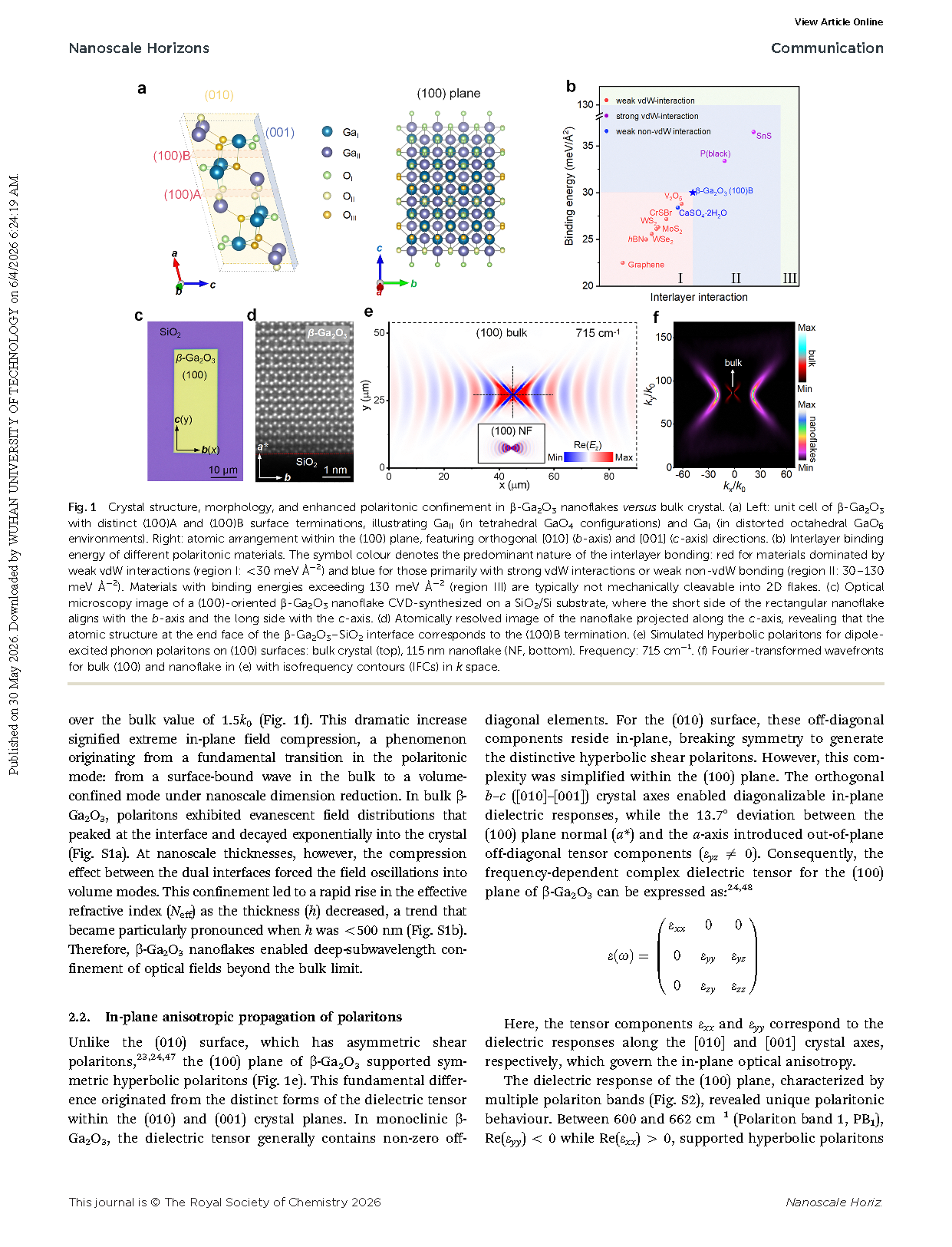
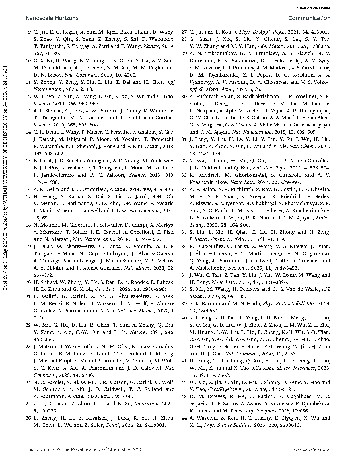
Figure 1 Crystal structure, morphology, and enhanced polaritonic confinement in β-Ga₂O₃ nanoflakes versus bulk crystal. (a) Left: unit cell of β-Ga₂O₃ with distinct (100) A and (100) B surface terminations, illustrating Ga in tetrahedral GaO₄ configurations and Ga in distorted octahedral GaO₆ environments). Right: atomic arrangement within the (100) plane, featuring orthogonal [010] (b-axis) and [001] (c-axis) directions. (b) Interlayer binding energy of different polaritonic materials. The symbol colour denotes the predominant nature of the interlayer bonding: red for materials dominated by weak vdW interactions (region I: <30 meV Å⁻²) and blue for those primarily with strong vdW interactions or weak non-vdW bonding (region II: 30–130 meV Å⁻². Materials with binding energies exceeding 130 meV Å⁻² (region III) are typically not mechanically cleavable into 2D flakes. (c) Optical microscopy image of a (100)-oriented β-Ga₂O₃ nanoflake CVD-synthesized on SiO₂/Si substrate, where the short side of the rectangular nanoflake aligns with the b-axis and the long side with the c-axis. (d) Atomically resolved image of the nanoflake projected along the c-axis, revealing that the atomic structure at the end face of the β-Ga₂O₃-SiO₂ interface corresponds to the (100) B termination. (e) Simulated hyperbolic polaritons for dipoleexcited phonon polaritons on (100) surfaces: bulk crystal (top), 115 nm nanoflake (NF, bottom). Frequency: 715 cm⁻¹. (f) Fourier-transformed wavefronts for bulk (100) and nanoflake in (e) with isofrequency contours (IFCs) in k space.
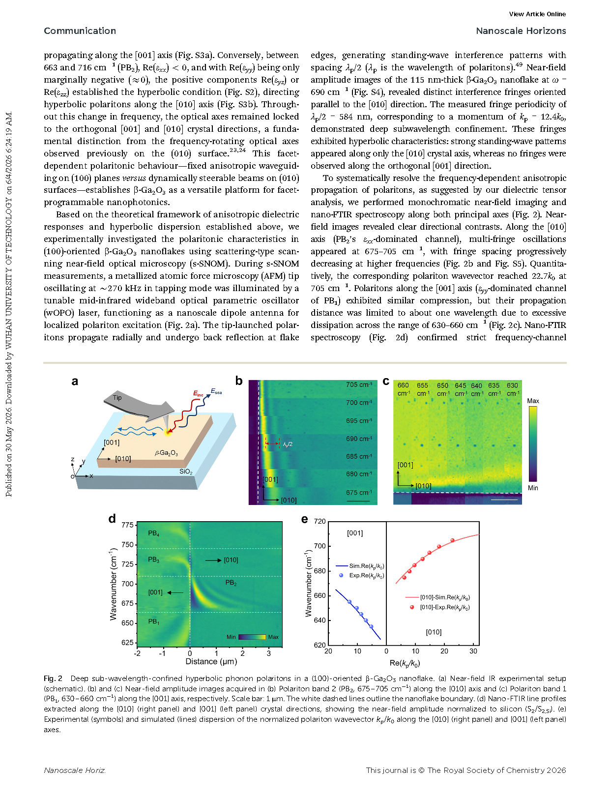
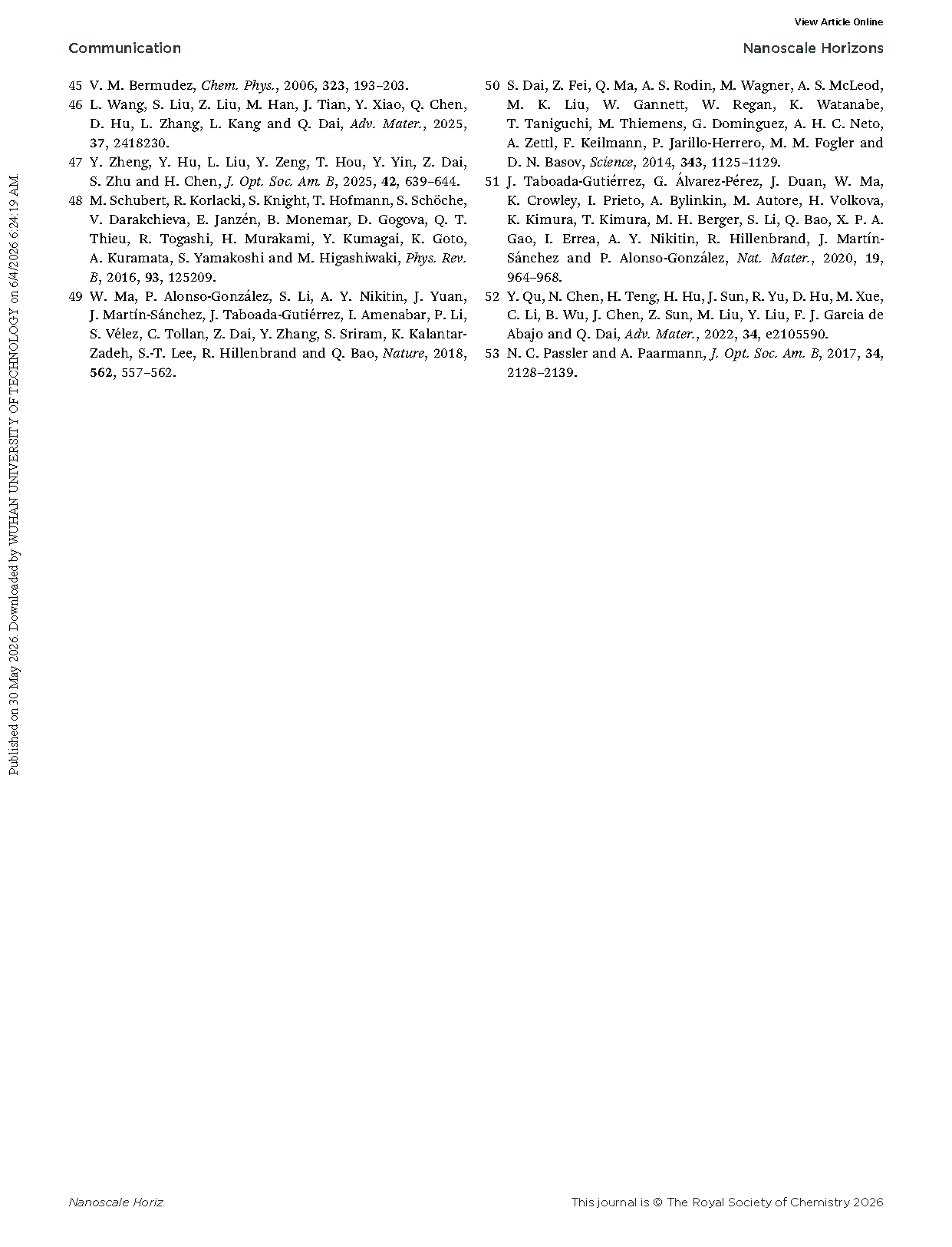
Figure 2 Deep sub-wavelength-confined hyperbolic phonon polaritons in a (100)-oriented β-Ga₂O₃ nanoflake. (a) Near-field IR experimental setup (schematic). (b) and (c) Near-field amplitude images acquired in (b) Polariton band 2 (PB₂, 675–705 cm⁻¹) along the [010] axis and (c) Polariton band 1 (PB₁, 630–660 cm⁻¹) along the [001] axis, respectively. Scale bar: 1 μm. The white dashed lines outline the nanoflake boundary. (d) Nano-FTIR line profiles extracted along the [010] (right panel) and [001] (left panel) crystal directions, showing the near-field amplitude normalized to silicon (S₂/S₂,Si). (e) Experimental (symbols) and simulated (lines) dispersion of the normalized polariton wavevector kₚ/k₀ along the [010] (right panel) and [001] (left panel) axes.
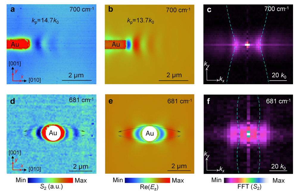
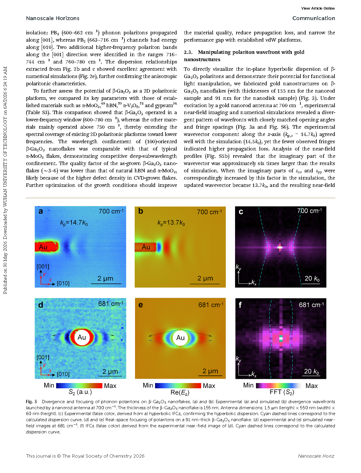
Figure 3 Divergence and focusing of phonon polaritons on β-Ga₂O₃ nanoflakes. (a) and (b) Experimental (a) and simulated (b) divergence wavefronts launched by a nanorod antenna at 700 cm⁻¹. The thickness of the β-Ga₂O₃ nanoflake is 155 nm. Antenna dimensions: 1.5 μm (length) 550 nm (width), 60 nm (height). (c) Experimental (false color, derived from a) hyperbolic IFCs, confirming the hyperbolic dispersion. Cyan dashed lines correspond to the calculated dispersion curve. (d) and (e) Real-space focusing of polaritons on a 91 nm-thick β-Ga₂O₃ nanoflake: (d) experimental and (e) simulated nearfield images at 681 cm⁻¹. (f) IFCs (false color) derived from experimental near-field image of (d). Cyan dashed lines correspond to the calculated dispersion curve.
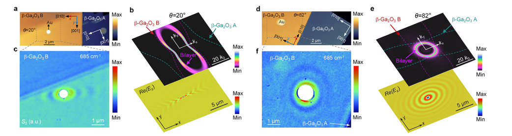
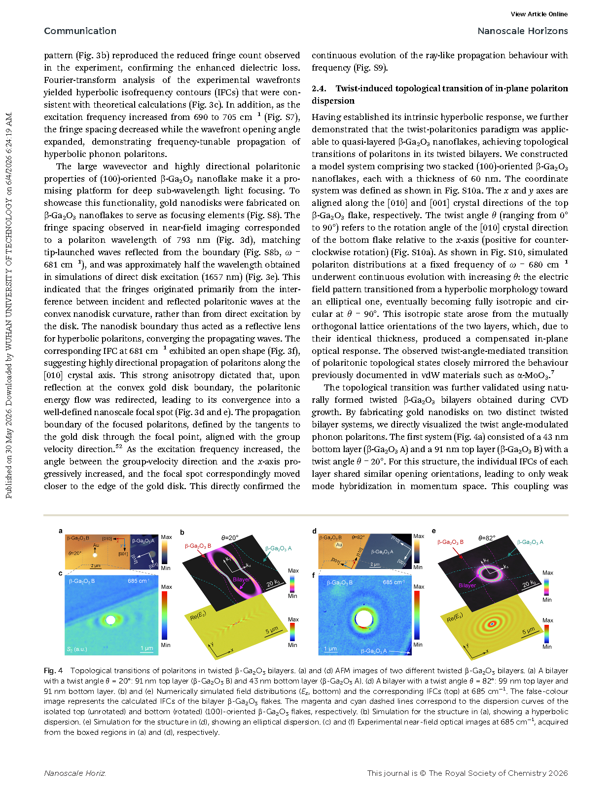
Figure 4 Topological transitions of polaritons in twisted β-Ga₂O₃ bilayers. (a) and (d) AFM images of two different twisted β-Ga₂O₃ bilayers. (a) A bilayer with a twist angle θ=20°: 91 nm top layer (β-Ga₂O₃ B) and 43 nm bottom layer (β-Ga₂O₃ A). (d) A bilayer with a twist angle θ=82°: 99 nm top layer and 91 nm bottom layer. (b) and (e) Numerically simulated field distributions (Ez, bottom) and the corresponding IFCs (top) at 685 cm⁻¹. The magenta and cyan dashed lines correspond to the dispersion curves of the isolated top (unrotated) and bottom (rotated) (100)-oriented β-Ga₂O₃ flakes. (b) Simulation for the structure in (a), showing a hyperbolic dispersion. (e) Simulation for the structure in (d), showing an elliptical dispersion. (c) and (f) Experimental near-field optical images at 685 cm⁻¹, acquired from the boxed regions in (a) and (d), respectively.
DOI:
10.1039/d6nh00044d