Paper Sharing
【Member Papers】Porous Ga₂O₃ and Defect Selective Etching via Electrochemical Path
日期:2026-06-09阅读:44
Researchers from the Zhejiang University have published a dissertation titled " Porous Ga2O3 and Defect Selective Etching via Electrochemical Path " in Semiconductor Science and Technology.
Background
β‑Ga₂O₃, as an ultra‑wide‑bandgap semiconductor (~4.8 eV), has great application potential in power devices and solar‑blind ultraviolet detection due to its high breakdown field strength, excellent thermochemical stability and high Baliga’s figure of merit. However, its high Ga‑O bond energy makes conventional etching require high temperature, high concentration acid or plasma dry etching, which is easy to introduce thermal stress, lattice damage and new defects, making it difficult to achieve controllable etching and accurate defect characterization at room temperature. Electrochemical etching relies on bias‑driven anodic dissolution without high temperature and high‑energy ion bombardment, resulting in lower damage, which is an ideal solution to realize controllable etching and defect revelation of β‑Ga₂O₃, but relevant research is still insufficient.
Abstract
β‑Ga₂O₃ is a promising ultra‑wide‑bandgap semiconductor for power and deep‑UV devices, yet its strong Ga–O bonds make controllable etching and defect delineation challenging. In this work, we systematically investigate the electrochemical etching of cast‑grown (100) β‑Ga₂O₃ substrates in 85 wt% phosphoric acid over an etching time range of 20–60 min and reveal a tunable transition from porous surface treatment to defect‑selective etching. At low anodic bias the etching proceeds in a time‑dependent reaction‑limited regime, where randomly distributed pores are formed on the surface. Additionally, above a critical bias (~15 V), etching becomes defect‑selective at room temperature, forming olive‑shaped surface pits aligned along the [010] direction, correlating strongly with dislocations, voids, and stress‑concentrated regions. It is demonstrated that the etching process is governed by the coupled kinetics of interfacial anodic dissolution and phosphate deposition–removal. This simple electrochemical strategy enables both porous structuring and defect revelation, offering a new route for substrate assessment and device engineering.
Highlights
Realize electrochemical porous etching of β‑Ga₂O₃ (100) plane at room temperature, obtaining uniform nanoporous structure with low damage and no degradation of electrical properties.
Break through the critical bias (~15 V) to achieve room‑temperature defect‑selective etching, accurately distinguishing three types of crystal defects: voids, strain and dislocations.
Clarify the coupled kinetics of anodic dissolution and phosphate deposition–removal, explaining the morphological transition mechanism from porous to defect‑selective etching.
The etching activation energy is only 0.073 eV, much lower than that of conventional wet etching, with mild process and strong controllability.
Conclusion
The team developed a phosphoric‑acid‑based electrochemical etching method that enables efficient etching of the (100) surface of β‑Ga₂O₃ at room temperature. When the applied bias is below the threshold voltage (~15 V), a porous surface morphology is formed. When the applied bias exceeds the threshold voltage, preferential dissolution at defect sites dominates over that at defect‑free regions, resulting in a defect‑selective etching morphology. Three types of etch pits (Types I, II, III) are resolved and correlated with voids, strain, and dislocations, respectively. The activation energy extracted at 20 V for the (100) surface is 0.073 eV. Compared to conventional wet etching, this electrochemical method provides sharper defect revelation with facile and tunable processing, while mitigating high‑temperature stress effects. Electrical characterization further supports the low‑added‑damage nature of the present process, as reflected by the nearly unchanged Hall transport parameters and the reduced reverse leakage in SBD devices. We further propose that the transition in etching morphology arises from the competition/coupling between anodic dissolution and phosphate deposition. Overall, this work establishes a reliable phosphoric‑acid‑based electrochemical etching route for β‑Ga₂O₃, where the etched surface morphology can be effectively tuned by the applied bias. The demonstrated voltage‑controlled transition from porous etching to defect‑selective etching provides a practical platform for device‑structure development and offers a new pathway for defect visualization, evaluation, and analysis in Ga₂O₃ substrates, while its potential for active device fabrication and surface engineering requires further studies on interface‑state control and phosphate‑residue management.
Project Support
National Key Research and Development Program of China (2024YFE0205300), the National Natural Science Foundation of China (22205203), the Zhejiang Provincial Postdoctoral Research Project Excellence Funding (ZJ2024079), the Natural Science Foundation of Zhejiang (LZ25E070001), the National Program for Support of Top‑notch Young Professionals, and the Leading Innovative and Entrepreneur Team Introduction Program of Hangzhou (TD2022012).
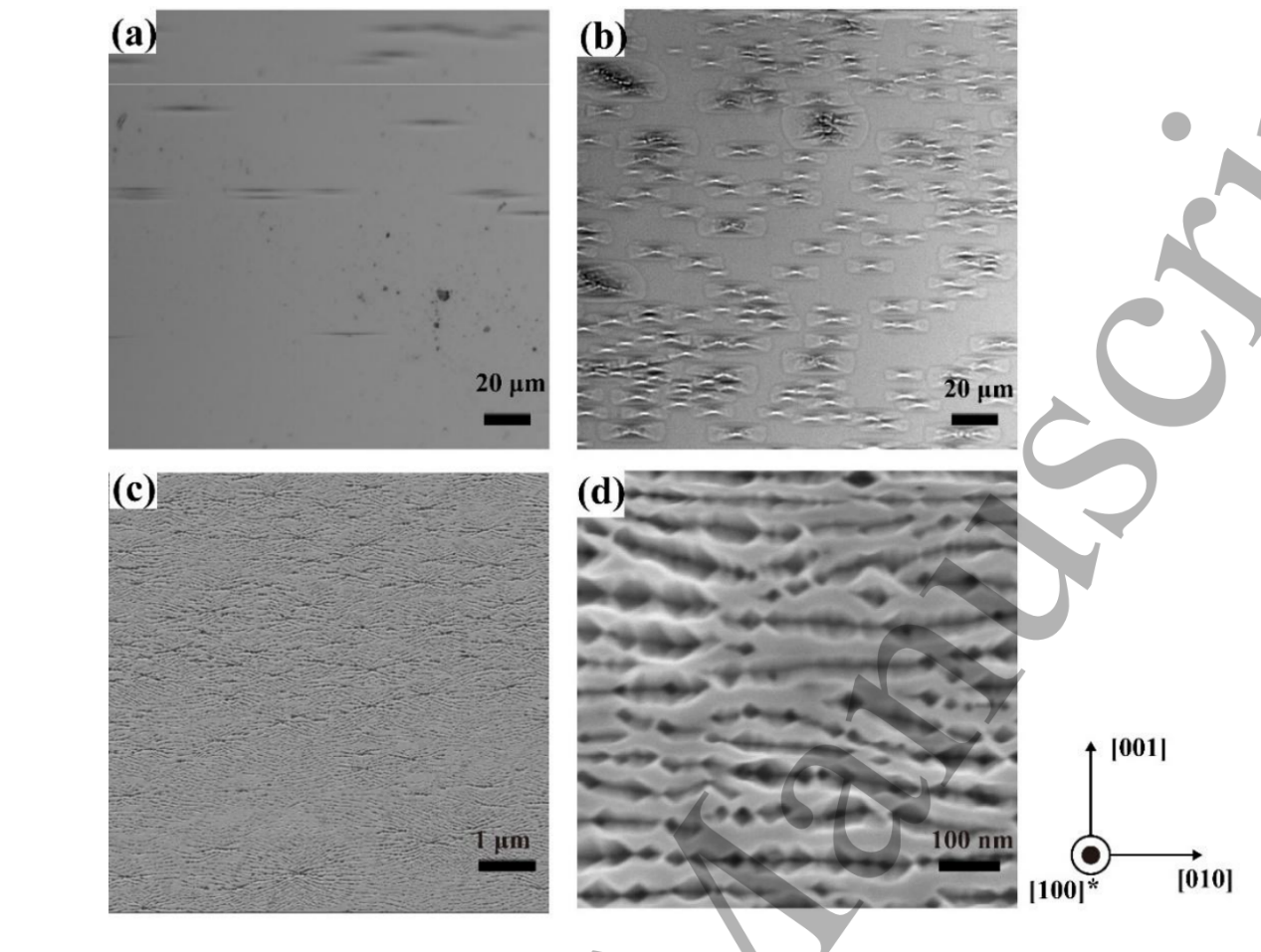
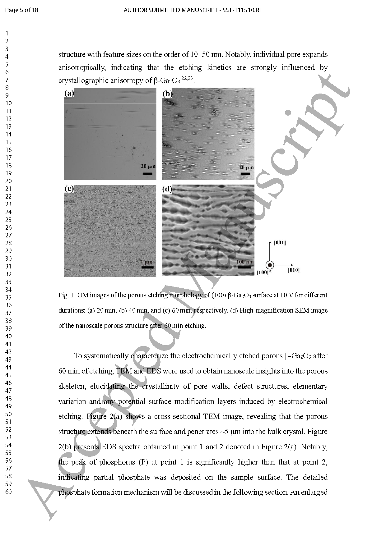
Fig. 1 OM images of the porous etching morphology of (100) β‑Ga₂O₃ surface at 10 V for different durations: (a) 20 min, (b) 40 min, and (c) 60 min, respectively. (d) High‑magnification SEM image of the nanoscale porous structure after 60 min etching.
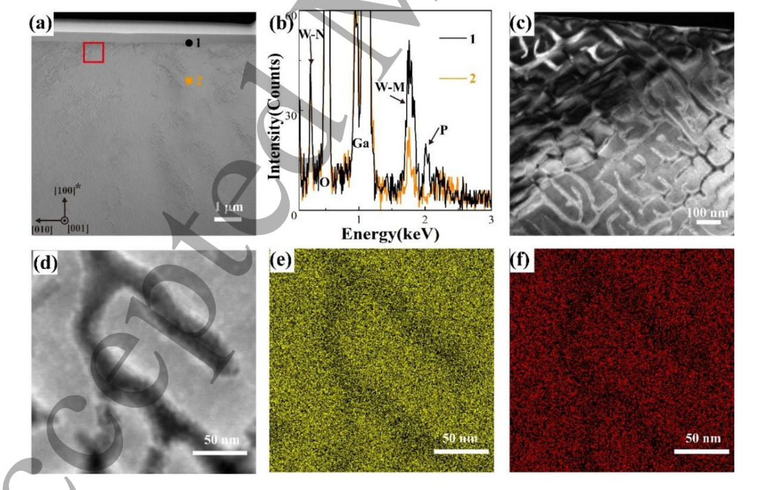
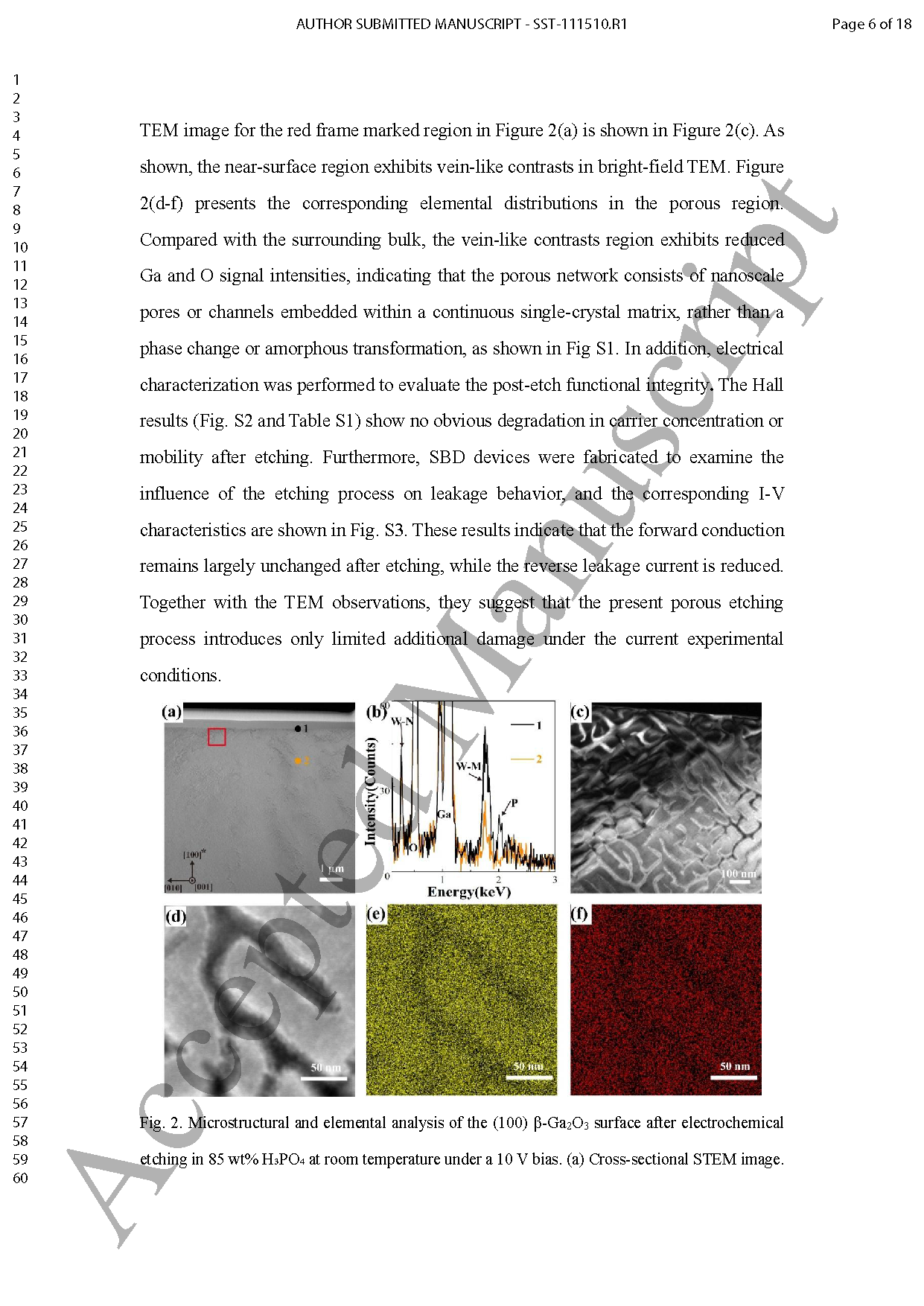
Fig. 2 Microstructural and elemental analysis of the (100) β‑Ga₂O₃ surface after electrochemical etching in 85 wt% H₃PO₄ at room temperature under a 10 V bias. (a) Cross‑sectional STEM image (b) EDS spectra obtained in point 1 and 2 marked in (a). (c) Bright‑field TEM image, highlighted by red frame marked region in (a). (d) High‑magnification TEM image and (e, f) EDS elemental mapping of Ga and O in (d), respectively.
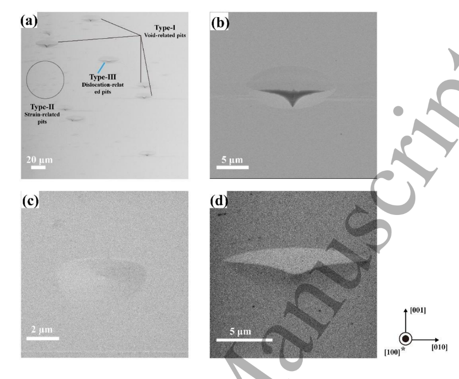
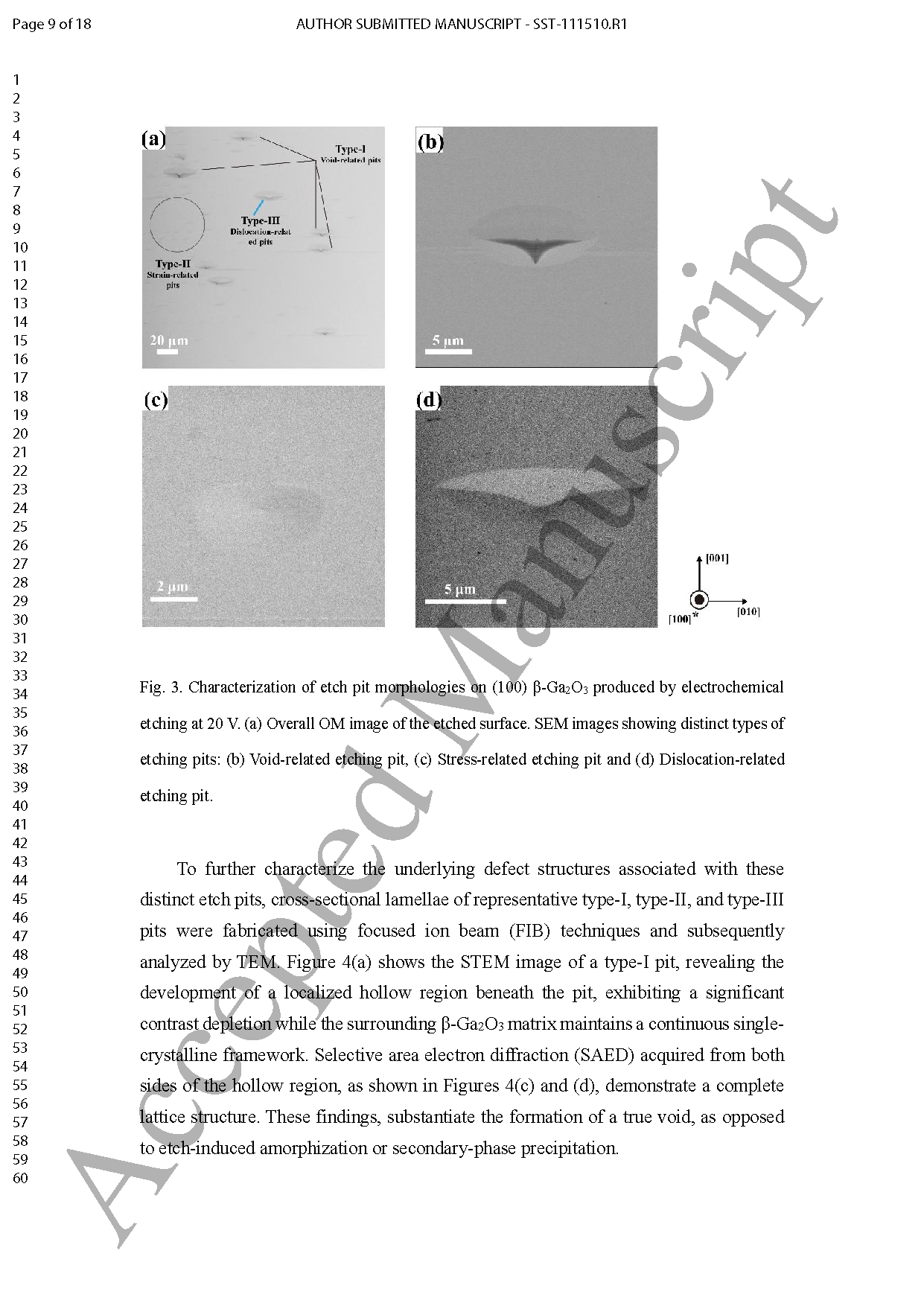
Fig. 3 Characterization of etch pit morphologies on (100) β‑Ga₂O₃ produced by electrochemical etching at 20 V. (a) Overall OM image of the etched surface. SEM images showing distinct types of etching pits: (b) Void‑related etching pit, (c) Stress‑related etching pit and (d) Dislocation‑related etching pit.
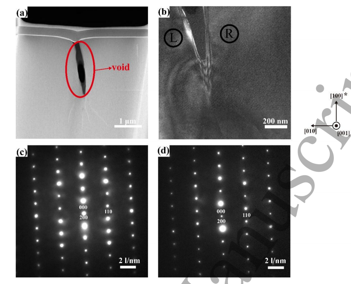
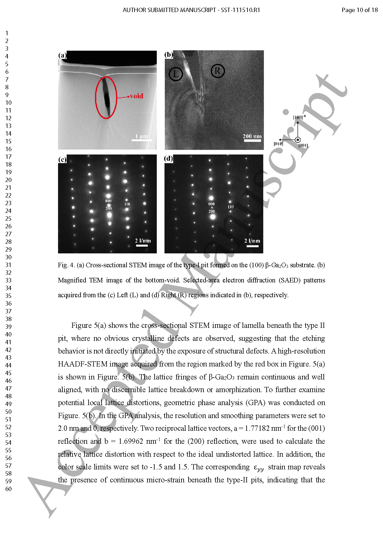
Fig. 4 (a) Cross‑sectional STEM image of the type‑I pit formed on the (100) β‑Ga₂O₃ substrate. (b) Magnified TEM image of the bottom‑void. Selected‑area electron diffraction (SAED) patterns acquired from the (c) Left (L) and (d) Right (R) regions indicated in (b), respectively.
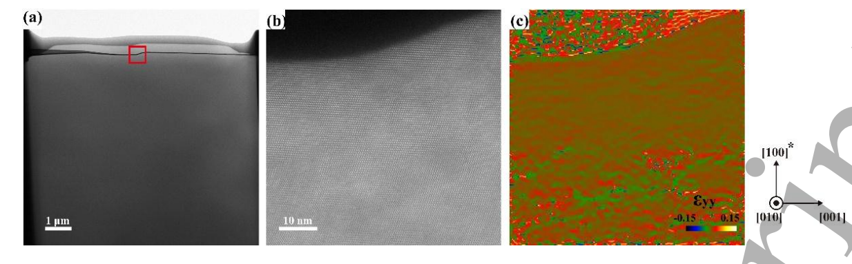
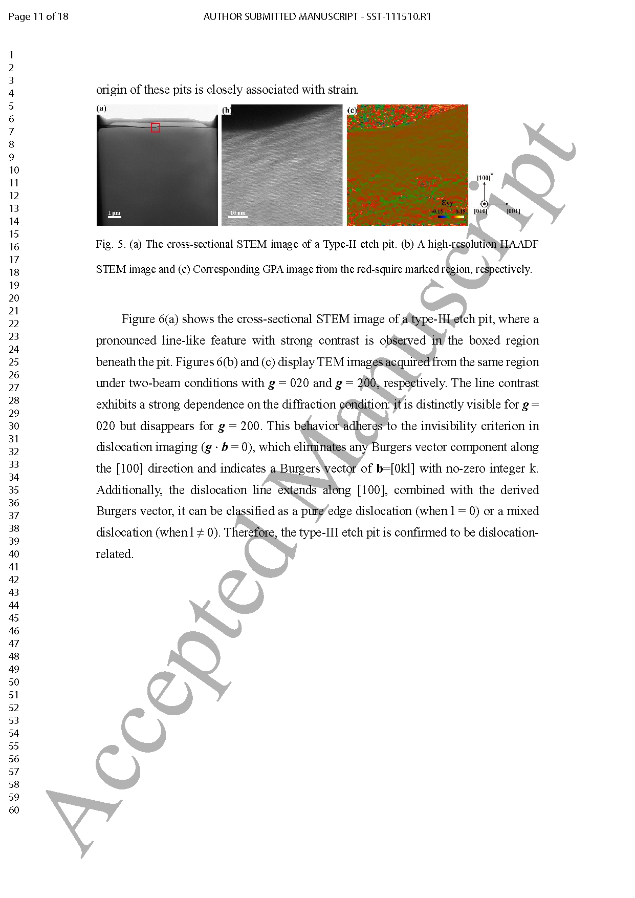
Fig. 5 (a) The cross‑sectional STEM image of a Type‑II etch pit. (b) A high‑resolution HAADF STEM image and (c) Corresponding GPA image from the red‑squire marked region, respectively.
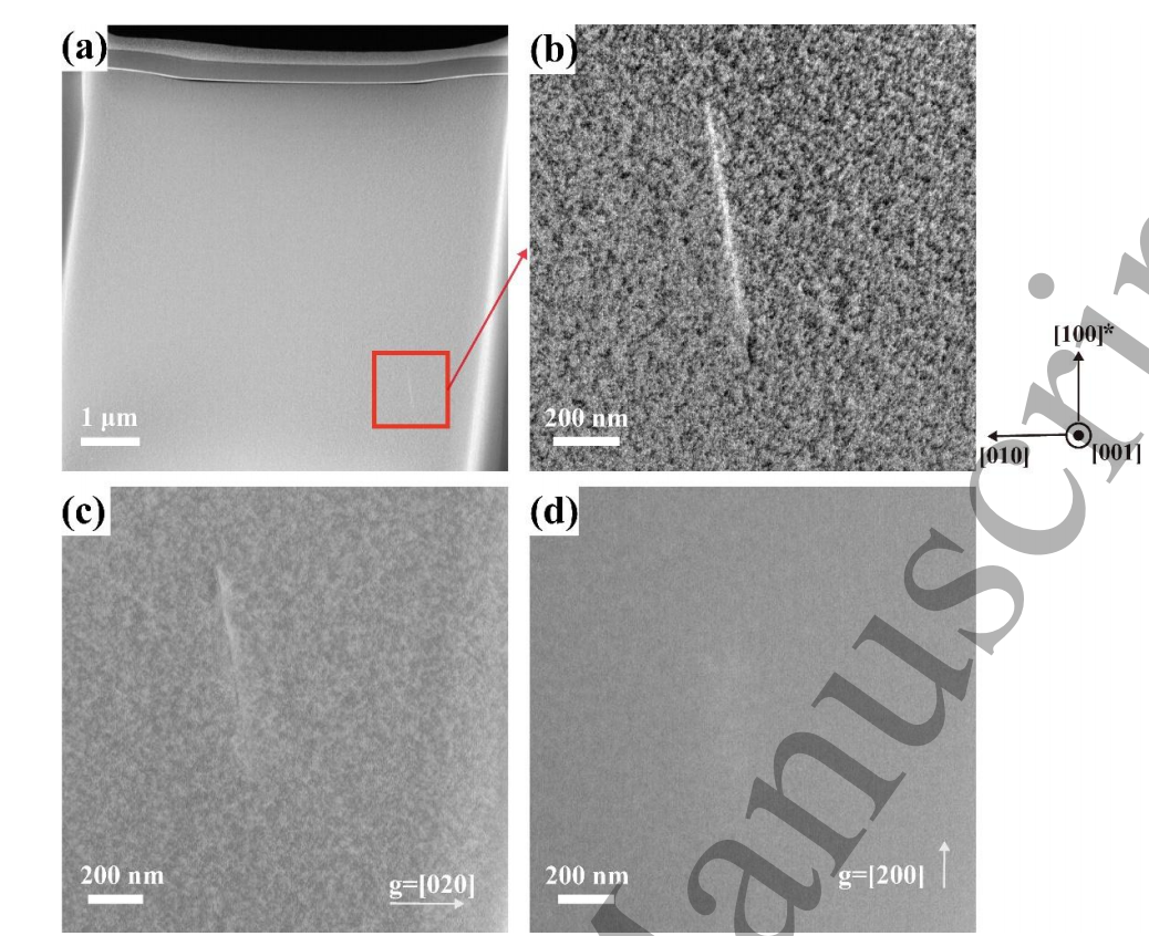
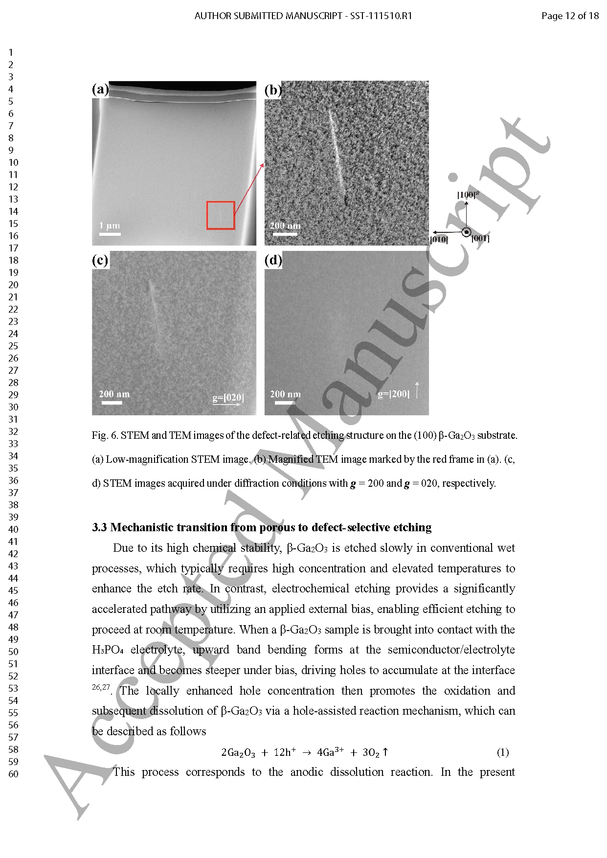
Fig. 6 STEM and TEM images of the defect‑related etching structure on the (100) β‑Ga₂O₃ substrate. (a) Low‑magnification STEM image. (b) Magnified TEM image marked by the red frame in (a). (c, d) STEM images acquired under diffraction conditions with g=200 and g=020, respectively.
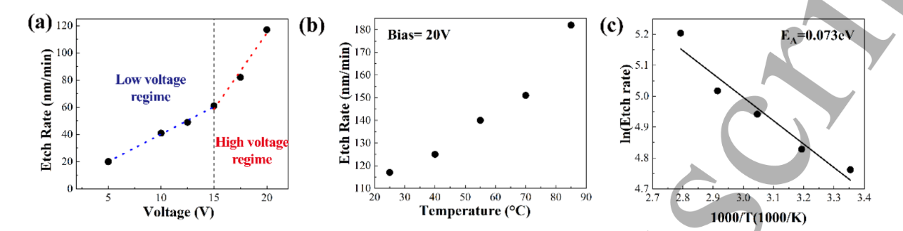
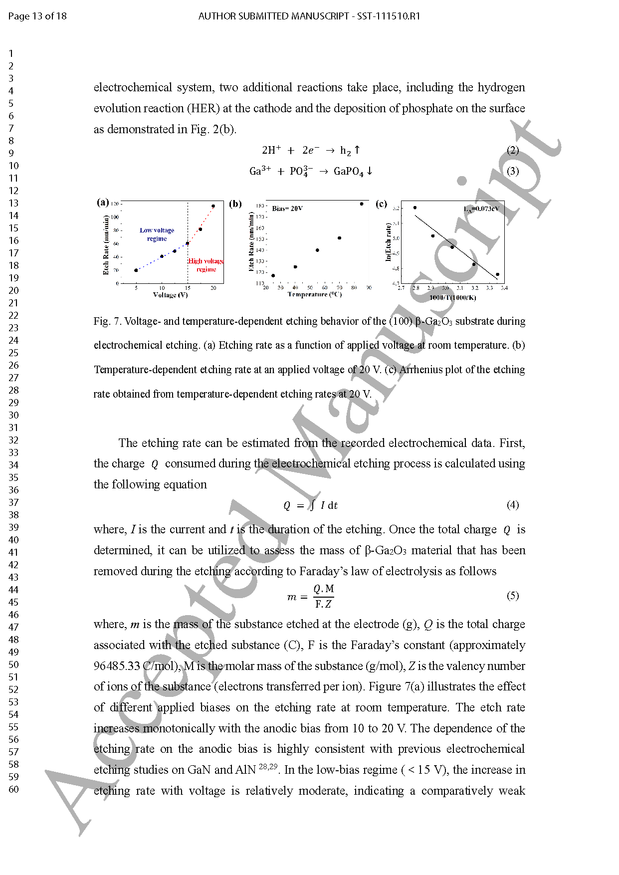
Fig. 7 Voltage‑ and temperature‑dependent etching behavior of the (100) β‑Ga₂O₃ substrate during electrochemical etching. (a) Etching rate as a function of applied voltage at room temperature. (b) Temperature‑dependent etching rate at an applied voltage of 20 V. (c) Arrhenius plot of the etching rate obtained from temperature‑dependent etching rates at 20 V.
DOI:
10.1088/1361-6641/ae7203