Paper Sharing
【Member Papers】One-Dimensional Wide-Bandgap Semiconductor β-Ga₂O₃ Nanorods for High-Performance Solar-Blind Ultraviolet Photodetectors
日期:2026-06-10阅读:30
Researchers from the Xidian University,Guilin University of Technology,Guilin University of Electronic Technology and Northwestern Polytechnical University have published a dissertation titled " One-Dimensional Wide-Bandgap Semiconductor β-Ga2O3 Nanorods for High-Performance Solar-Blind Ultraviolet Photodetectors " in Nanoscale.
Background
Solar-blind ultraviolet (UV) detection (200–280 nm) is indispensable for flame sensing, missile warning, ozone monitoring, space communications and other fields. Devices require high sensitivity, low dark current, fast response and compatibility with low-cost and scalable fabrication. As an ultra-wide-bandgap semiconductor (~4.8 eV), β‑Ga₂O₃ can completely suppress visible/near-UV absorption and is naturally suitable for the 254 nm solar-blind band, with high breakdown field strength and excellent chemical and thermal stability. One-dimensional nanorod structure is an ideal structure for high-performance optoelectronic devices due to its high aspect ratio which can enhance light absorption and carrier transport efficiency. Existing preparation methods of one-dimensional β‑Ga₂O₃ are mostly complex and difficult to scale. Low-pressure chemical vapor deposition (LPCVD) is simple and suitable for large-area growth, but the deposited products generally have oxygen vacancy defects, which increase background carrier concentration, dark current, and introduce trap states leading to slow response and persistent photoconductivity. Regulating the photoelectric properties of materials through oxygen vacancy defect engineering is a key way to realize high-performance solar-blind UV photodetectors.
Abstract
Solar-blind ultraviolet photodetectors require wide-bandgap materials that can be synthesized through simple and scalable processes. In this work, we demonstrate the controlled growth and defect engineering of β-Ga₂O₃ nanorod films for high-performance detection. Nanorods were synthesized on SiO₂/Si substrates by low-pressure chemical vapor deposition using gallium and oxygen, followed by post-growth oxygen annealing. Structural characterization confirms a highly crystalline monoclinic β phase, and surface chemistry analysis shows that the vacancy-related O 1s component is significantly reduced after annealing. Under 254 nm illumination, metal–semiconductor–metal photodetectors based on annealed nanorods deliver a dark current on the order of 10⁻¹⁰ A, a photo-to-dark current ratio up to 6×10³, and fast rise/decay times of 0.30/1.61 s. These performance enhancements are attributed to effective vacancy passivation, which reduces free-carrier background, mitigates trap-assisted recombination, and improves carrier transport in the nanorod film. Overall, this work establishes LPCVD combined with oxygen annealing as a cost-effective and scalable route to β-Ga₂O₃-based solar-blind photodetectors and provides practical insight into defect engineering strategies for wide-bandgap oxide semiconductors.
Highlights
High-crystallinity and interwoven porous one-dimensional β‑Ga₂O₃ nanorod films are controllably prepared on SiO₂/Si substrates by LPCVD with simple and scalable process.
High-temperature oxygen annealing is proposed to achieve efficient passivation of oxygen vacancies, reducing the vacancy-related O 1s component from 23.66% to 8.25% without changing the phase and morphology.
The dark current of the passivated detector is suppressed to 10⁻¹⁰ A, the photo-to-dark current ratio is increased to 6×10³, and the rise/decay time reaches 0.30/1.61 s with significantly improved response speed.
The correlation mechanism of oxygen vacancy-carrier transport-photoelectric performance is established, providing a universal strategy for defect regulation of wide-bandgap oxide solar-blind detectors.
Conclusion
Cost-effective LPCVD was used to form randomly oriented β-Ga₂O₃ nanorod films that interweave into a porous layer on Si/SiO₂; SEM and EDS analyses confirm film-scale morphology and Ga/O distribution, and HRTEM resolves lattice spacings of 0.187, 0.236, and 0.197 nm indexed to the (510), (−311), and (−312) planes of monoclinic β-Ga₂O₃. XRD together with Raman verifies the β phase and shows phase retention after oxygen annealing. O 1s XPS reveals a marked decrease of the vacancy-related component, indicating effective oxygen-vacancy passivation. MSM devices fabricated on the annealed films exhibit a suppressed dark current of ~10⁻¹⁰ A and a photo-to-dark current ratio of 6×10³ at 254 nm under 254 nm illumination and 10 V, with fast rise/decay times of 0.30 s/1.61 s. Together, these results demonstrate that combining LPCVD growth with oxygen annealing provides a scalable and effective approach to linking defect control at the materials level with enhanced device performance, offering a practical pathway toward high-performance solar-blind deep-UV photodetectors.
Project Support
National Natural Science Foundation of China (Grant Nos. 62574159, 62090033, 62293522); Zhejiang Provincial Natural Science Foundation of China (LDT23F0402, LDT23F04024F04); Key Research and Development Program of Shaanxi (Grant No. 2025GHYBXM-050); China National Postdoctoral Programme for Innovative Talents (BX20230281); Xidian University Specially Funded Project for Interdisciplinary Exploration (TZJH2024064); China Postdoctoral Science Foundation (Certificate Number: 2024M752520); Natural Science Foundation of Fujian (No. 2025J01327); Fuzhou Science and Technology Project (2024-SG-008); Fuzhou Institute of Oceanography project (No. 2024F17).
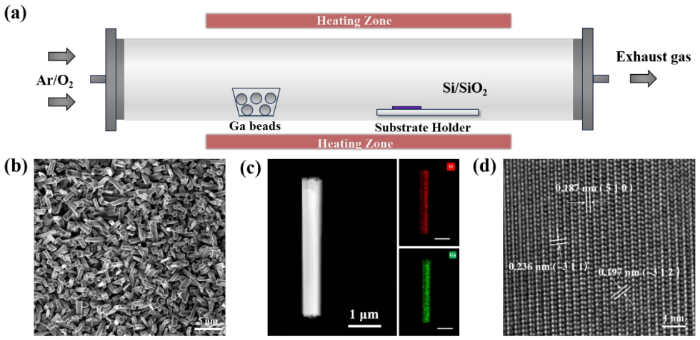
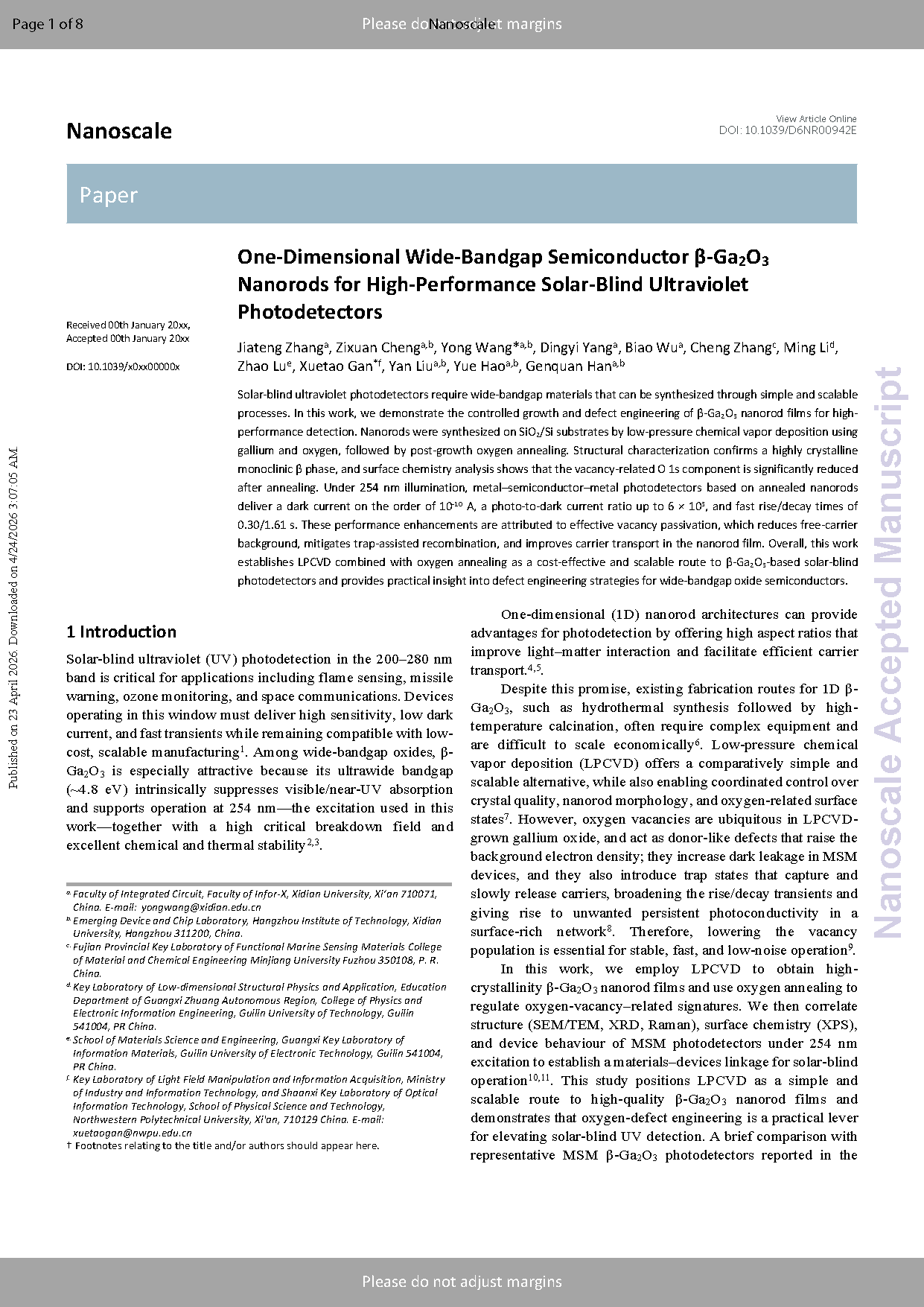
Fig. 1 (a) Schematic of the LPCVD growth for β-Ga₂O₃ nanorod films on SiO₂/Si (b) SEM image of β-Ga₂O₃ nanorod films. (c) EDS elemental maps of Ga and O corresponding to a nanorod. (d) HRTEM image of a nanorod.
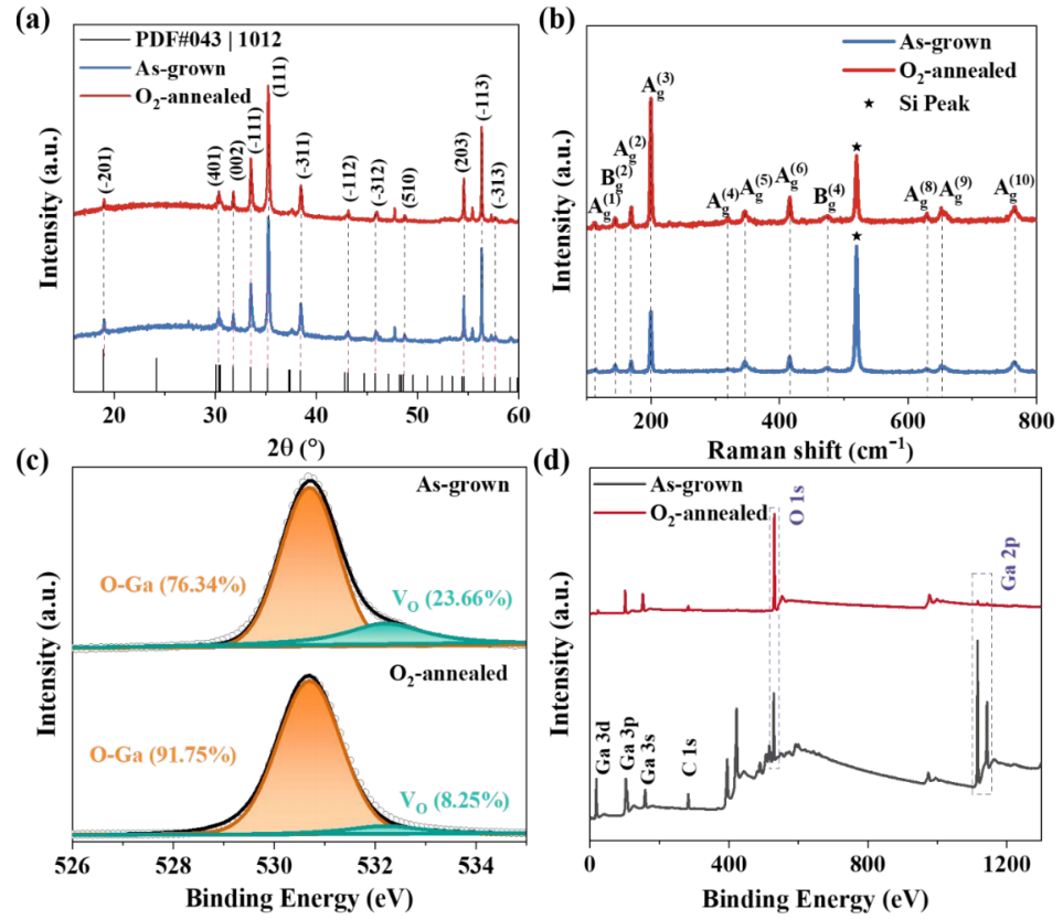
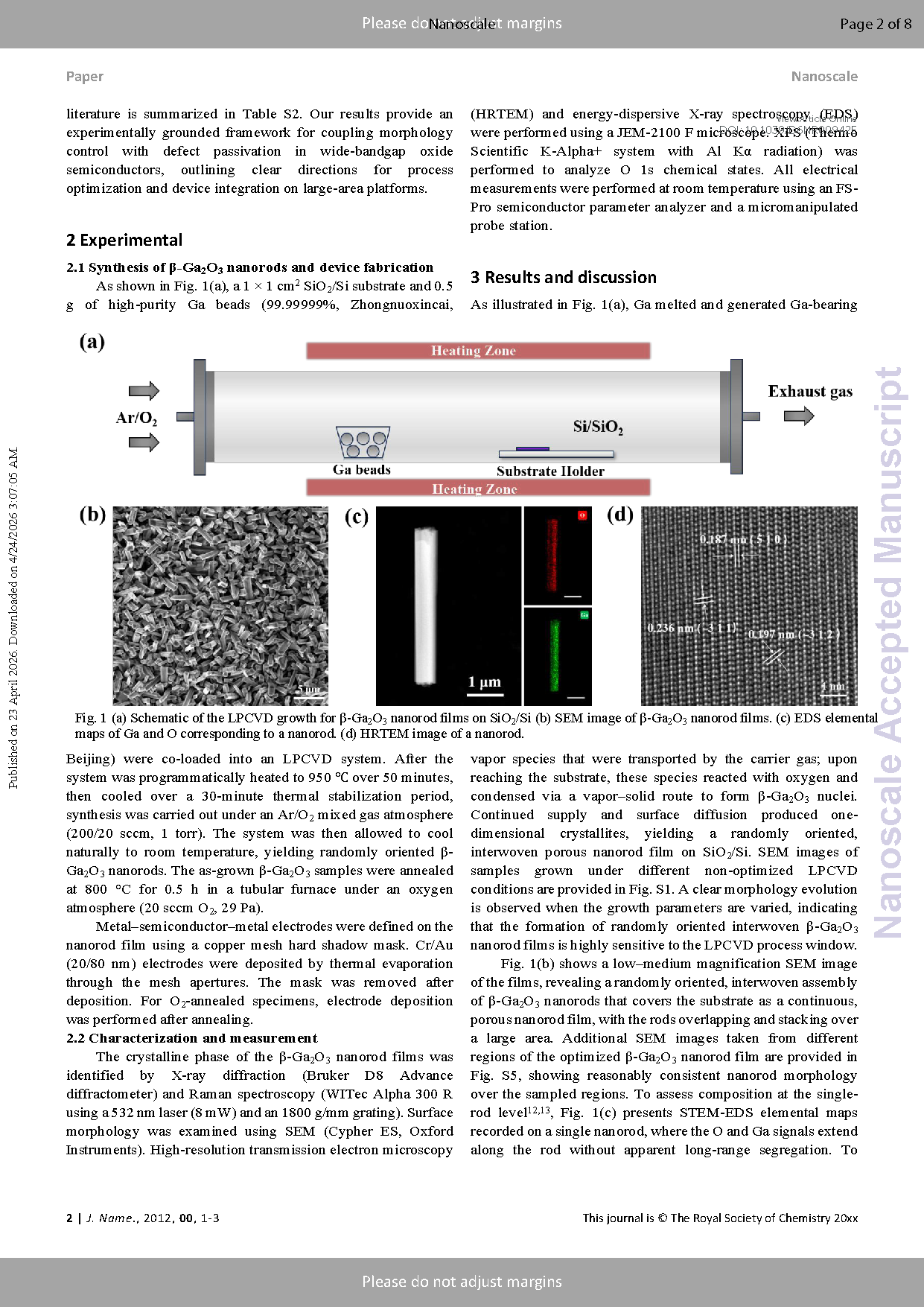
Fig. 2 (a) X-ray diffraction (XRD) patterns of as-grown and O₂-annealed β-Ga₂O₃ nanorod films. (b) Raman spectra of β-Ga₂O₃ nanorod films. (c) O 1s XPS spectra of the as-grown and O₂-annealed films. (d) XPS survey spectra of β-Ga₂O₃ nanorods before and after annealing in an oxygen atmosphere.
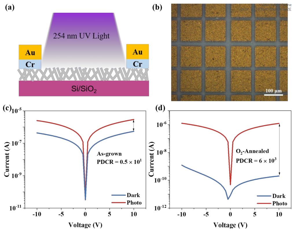
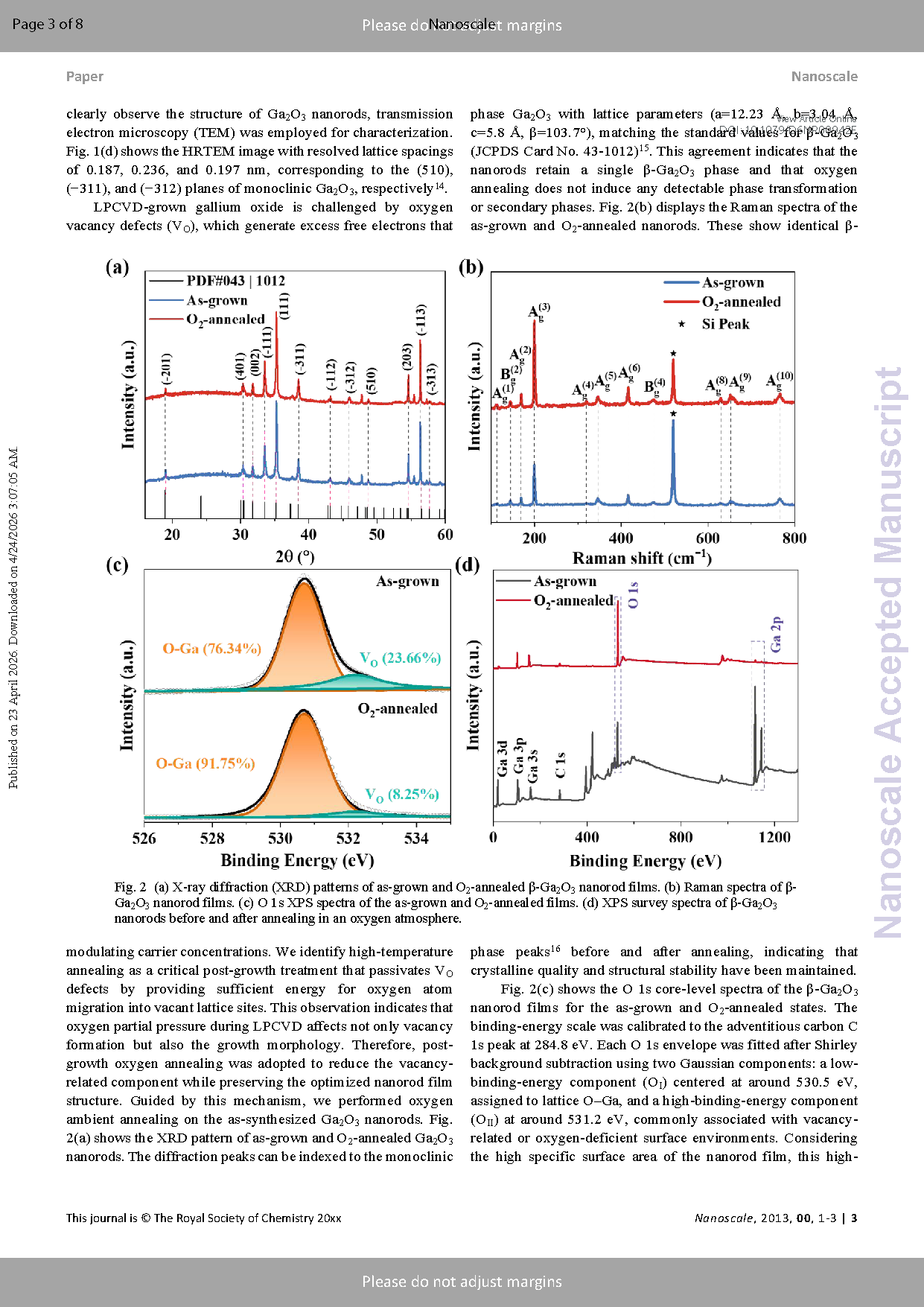
Fig. 3 (a) Schematic of the MSM photodetector. (b) Optical micrograph of the device array. (c) I–V characteristics of the as-grown and (d) the O₂-annealed device in the dark and under 254 nm illumination.
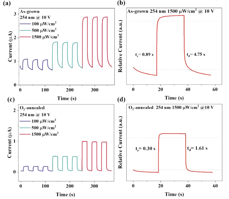
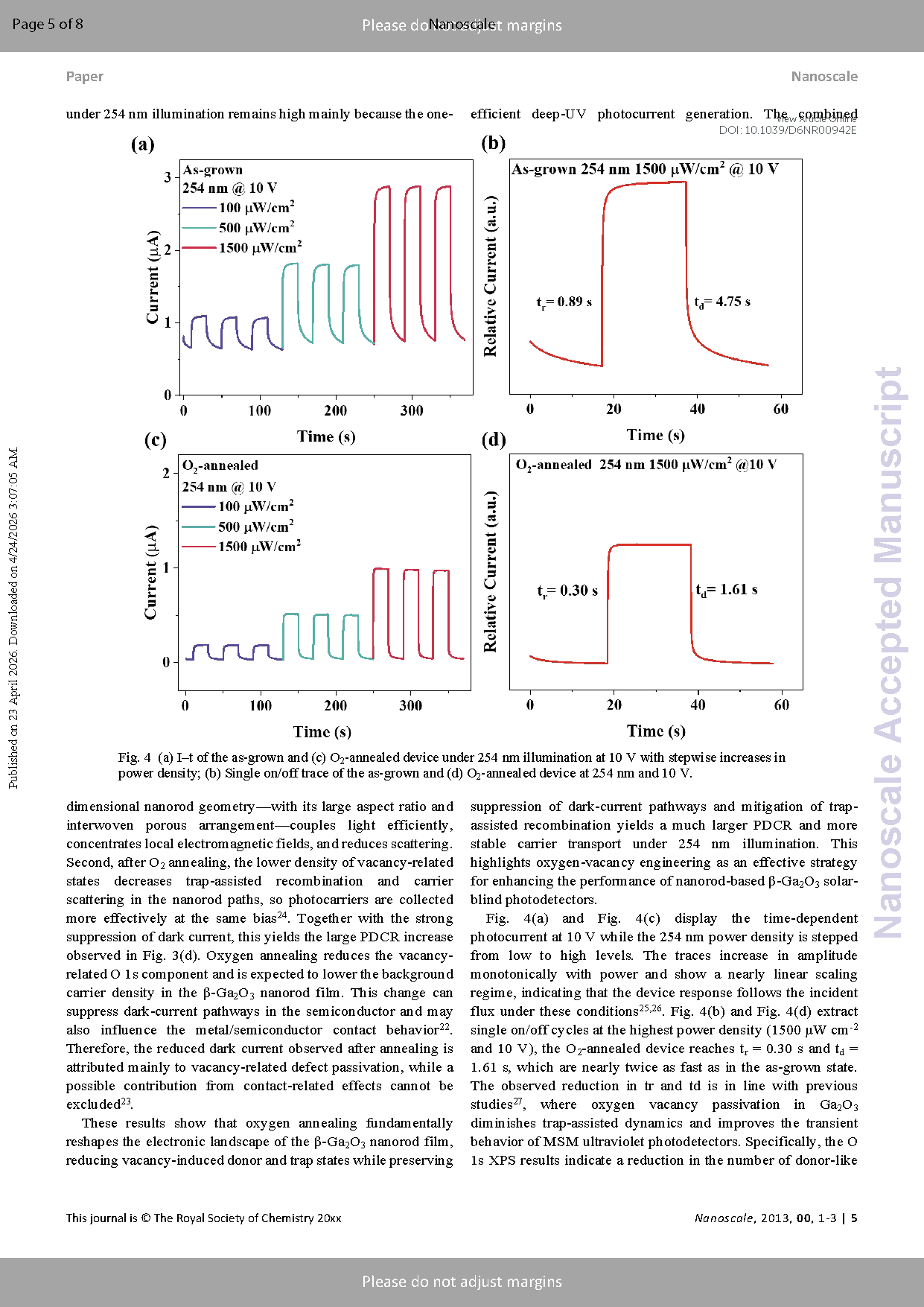
Fig. 4 (a) I–t of the as-grown and (c) O₂-annealed device under 254 nm illumination at 10 V with stepwise increases in power density; (b) Single on/off trace of the as-grown and (d) O₂-annealed device at 254 nm and 10 V.
DOI :
10.1039/D6NR00942E