Paper Sharing
【International Papers】Single-Crystalline High-Quality β-Ga₂O₃ Pseudosubstrate on Sapphire through Sputtering for Epitaxial Deposition
日期:2026-06-11阅读:12
Researchers from University of Wisconsin-Madison, University of Massachusetts Lowell, University of New Mexico, Agnitron Technology Incorporated have published a dissertation titled "Single-Crystalline High-Quality β-Ga₂O₃ Pseudosubstrate on Sapphire through Sputtering for Epitaxial Deposition" in ACS Applied Engineering Materials.
Background
β-Ga₂O₃ features an ultra-wide bandgap of ~4.8 eV and ultrahigh breakdown electric field, serving as promising candidate for high-power electronics and solar-blind photodetectors widely used in power grid and aerospace industry. Bulk β-Ga₂O₃ single crystal is expensive and large-size wafers are undeveloped, making heteroepitaxy on sapphire an economical alternative. Direct MOCVD/MBE growth on sapphire suffers severe lattice mismatch, resulting in miscellaneous phases, high defects and degraded electrical performance. RF sputtering is cost-effective for large-area coating yet normally produces amorphous Ga₂O₃, which cannot act as epitaxial template for subsequent CVD growth. Few available sputtering-derived single-crystal pseudosubstrate has been reported, leaving an important research gap in low-cost high-quality β-Ga₂O₃ epitaxy.
Abstract
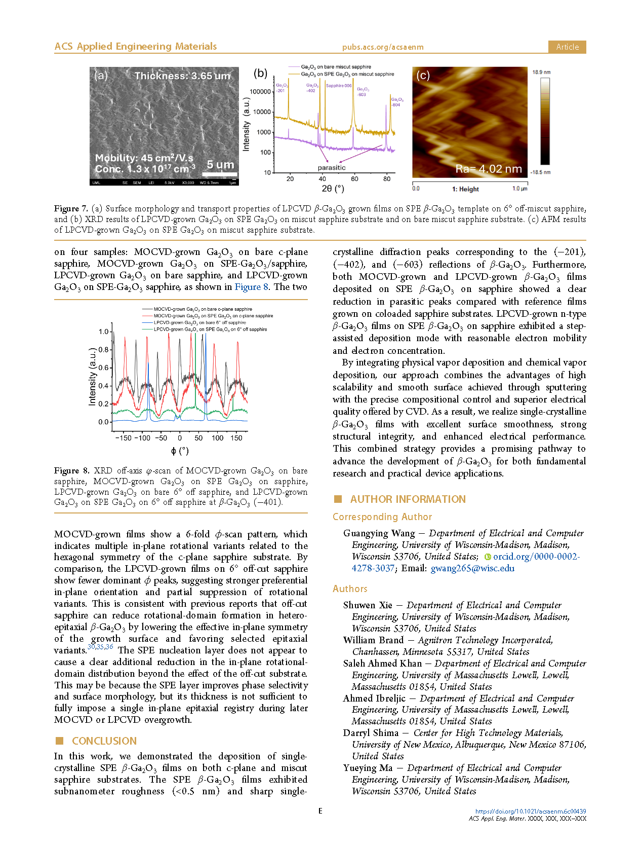
Solid-phase epitaxy (SPE) of β-Ga₂O₃ thin films by radio frequency (RF) sputtering, followed by high-temperature postdeposition annealing, is employed on sapphire substrates, yielding a high-quality pseudosubstrate for subsequent buffer growth via MOCVD and LPCVD. Low roughness (<0.5 nm) and sharp single-crystalline diffraction peaks corresponding to the (-201), (-402), and (-603) reflections of β-Ga₂O₃ were observed in the SPE β-Ga₂O₃ film and the subsequent epitaxial buffer layer. N-doped Ga₂O₃ film grown by LPCVD on SPE Ga₂O₃ film showed step-assisted growth mode with reasonable electronic behavior, with 45 cm²/V·s mobility at a bulk carrier concentration of 1.3 ×10¹⁷ cm⁻³. These results suggest that SPE Ga₂O₃ is a promising pathway to advance the development of β-Ga₂O₃ on foreign substrates.
Highlights
Combine RF sputtering and high-temperature annealing to realize SPE single-crystal β-Ga₂O₃ pseudosubstrate on sapphire.
The as-fabricated SPE template has surface roughness below 0.5 nm and pure β-phase crystalline property.
The pseudosubstrate effectively suppresses miscellaneous phase during follow-up MOCVD/LPCVD epitaxy.
LPCVD-grown n-Ga₂O₃ on SPE layer obtains mobility of 45 cm²/V·s at 1.3×10¹⁷ cm⁻³ carrier concentration.
Conclusion
In this work, we demonstrated the deposition of single-crystalline SPE β-Ga₂O₃ films on both c-plane and miscut sapphire. The SPE β-Ga₂O₃ films exhibited subnanometer roughness (<0.5 nm) and sharp single-crystalline diffraction peaks corresponding to the (-201), (-402), and (-603) reflections of β-Ga₂O₃. Furthermore, both MOCVD-grown and LPCVD-grown β-Ga₂O₃ films deposited on SPE β-Ga₂O₃ showed a clear reduction in parasitic peaks compared with reference films grown on bare sapphire. LPCVD-grown n-type β-Ga₂O₃ on SPE exhibited a step-assisted deposition mode with reasonable electron mobility and electron concentration.
By integrating physical vapor deposition and chemical vapor deposition, our approach combines the advantages of high scalability and smooth surface achieved through sputtering with precise compositional control offered by CVD. This combined strategy provides a promising pathway to advance the development of β-Ga₂O₃ for both fundamental research and practical device applications.
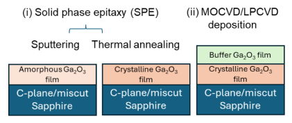
Figure 1. Schematic illustration of the two-step growth pathway: (i) formation of crystalline β-Ga₂O₃ on sapphire by SPE, followed by (ii) deposition of the β-Ga₂O₃ buffer layer by MOCVD or LPCVD.
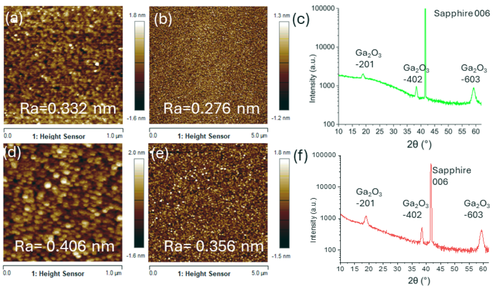
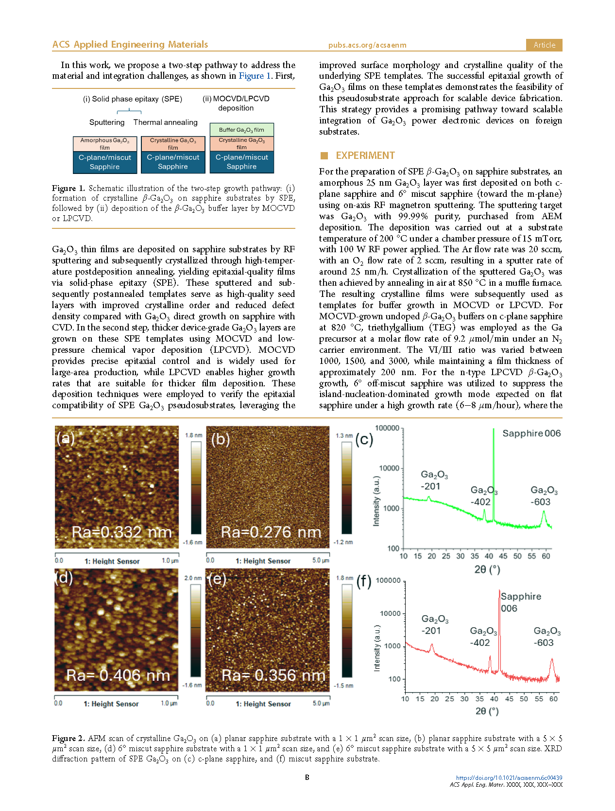
Figure 2. AFM scan of crystalline Ga₂O₃ on (a) planar sapphire substrate with a 1 ×1 μm² scan size, (b) planar sapphire substrate with a 5 ×5 μm² scan size, (d) 6° miscut sapphire substrate with a 1 ×1 μm² scan size, and (e) 6° miscut sapphire substrate with a 5 ×5 μm² scan size. XRD diffraction pattern of SPE Ga₂O₃ on (c) c-plane sapphire, and (f) miscut sapphire substrate.
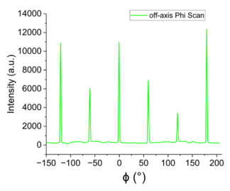
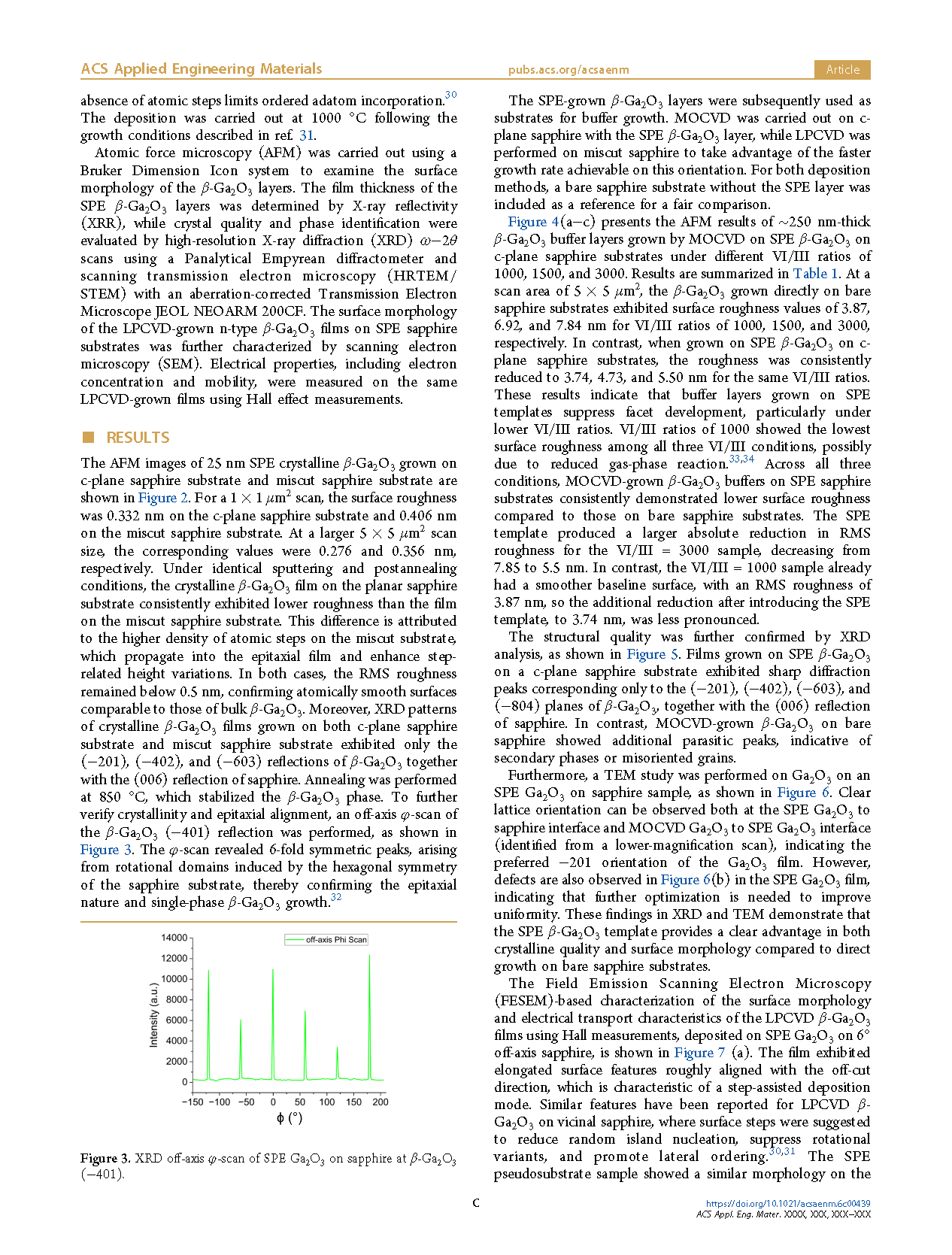
Figure 3. XRD off-axis φ-scan of SPE Ga₂O₃ on sapphire at β-Ga₂O₃ (-401).
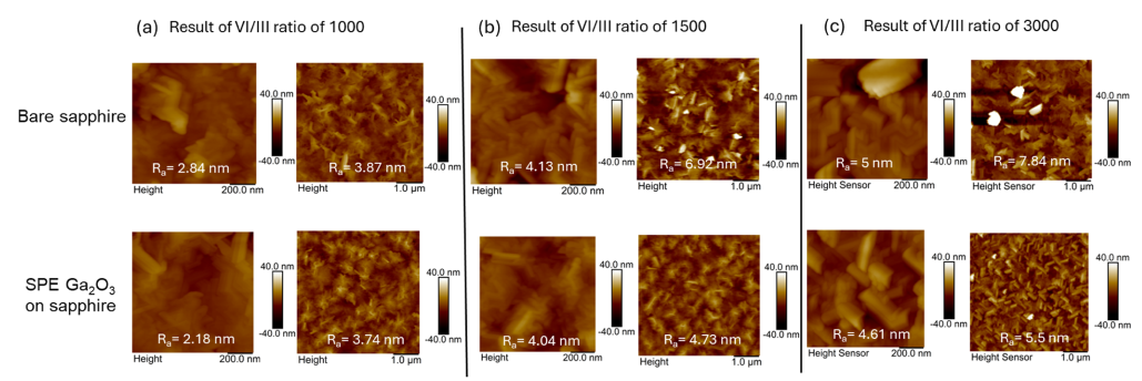
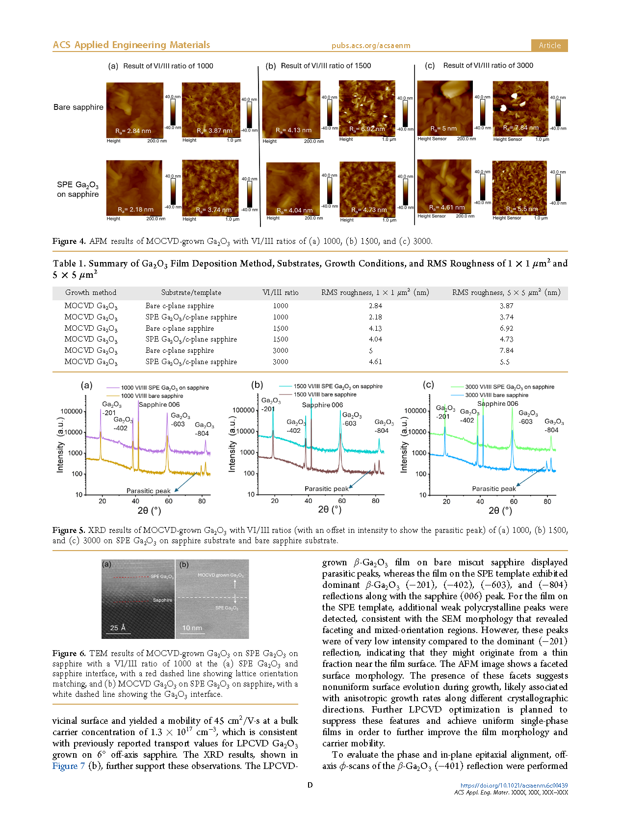
Figure 4. AFM results of MOCVD-grown Ga₂O₃ with VI/III ratios of (a) 1000, (b) 1500, and (c) 3000.
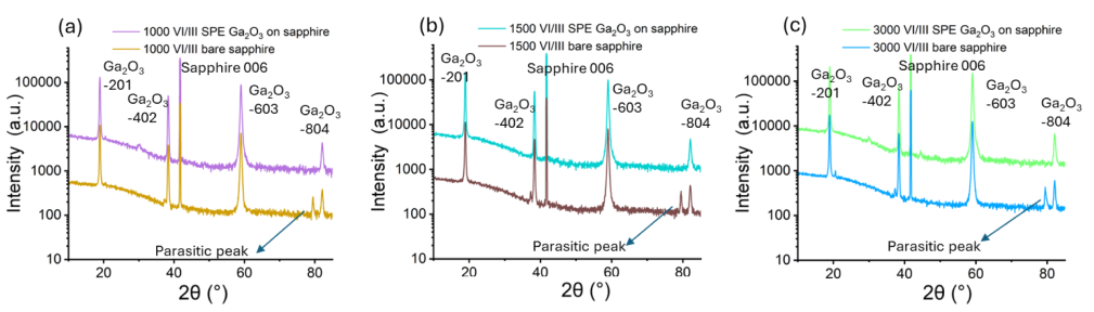
Figure 5. XRD results of MOCVD-grown Ga₂O₃ with VI/III ratios (with an offset in intensity to show the parasitic peak) of (a) 1000, (b) 1500, and (c) 3000 on SPE Ga₂O₃ on sapphire substrate and bare sapphire substrate.
DOI:
doi.org/10.1021/acsaenm.6c00439