Paper Sharing
【Member Papers】High Schottky barrier formation in tilted-dipole PdCoO₂/β-Ga₂O₃ (001) interfaces
日期:2026-06-11阅读:10
Researchers from National Institute for Materials Science, Novel Crystal Technology, Inc have published a dissertation titled "High Schottky barrier formation in tilted-dipole PdCoO₂/β-Ga₂O₃ (001) interfaces" in Applied Physics Letters.
Background
β-Ga₂O₃ is an ultra-wide-bandgap semiconductor with a bandgap of 4.6–5.0 eV, featuring high breakdown field, outstanding chemical stability and scalable single-crystal growth via melt method, which is promising for high-voltage Schottky diodes and high-temperature FETs. Large Schottky barrier can suppress thermally induced leakage and boost reverse blocking performance under high-temperature operation. Traditional Pt/Ni metal contacts only form limited barrier height. Layered PdCoO₂ generates intrinsic interfacial dipole to increase barrier, while previous researches are limited to β-Ga₂O₃ (201). The (001) plane is superior for high-quality homoepitaxy and high-power chips, yet the barrier property under tilted polarization direction remains unstudied.
Abstract
We report the growth and Schottky junction characteristics of metallic delafossite PdCoO₂/β-Ga₂O₃ (001) heterostructures. The PdCoO₂ thin films predominantly grow with the epitaxial relationship of PdCoO₂ (006)//β-Ga₂O₃ (202), forming a high-quality oxide–oxide interface. Despite a 24°tilt between the PdCoO₂ surface polarization axis and the β-Ga₂O₃ (001) surface normal, a large Schottky barrier height of φbJV >1.7 eV was achieved. This value is comparable with that reported for PdCoO₂/β-Ga₂O₃ (201) where the PdCoO₂ surface polarization axis is perpendicular to the interface. The PdCoO₂/β-Ga₂O₃ junction showed a large on–off ratio of ~10⁸ at 573 K. These results demonstrate the feasibility of delafossite-type electrodes for β-Ga₂O₃ (001) heterostructures with high-quality homoepitaxial layers.
Highlights
Realize epitaxial growth of PdCoO₂ on β-Ga₂O₃ (001) substrate with PdCoO₂ (006)//β-Ga₂O₃ (202) orientation.
Obtain over 1.7 eV Schottky barrier under 24° tilted interfacial dipole condition.
The fabricated diode achieves ~10⁸ on-off ratio at 573 K high temperature environment.
Verify PdCoO₂ is available as high-barrier electrode for β-Ga₂O₃ (001) high-power devices.
Conclusion
In summary, we fabricated heterostructures of the conductive layered oxide PdCoO₂ and β-Ga₂O₃ (001).The PdCoO₂ thin film was found to grow dominantly with the epitaxial relationship of PdCoO₂ (006)//β-Ga₂O₃ (202),with the PdCoO₂ surface polarization direction tilted by 24°from the β-Ga₂O₃ (001) surface normal. Nevertheless, a large Schottky barrier height exceeding 1.7 eV was obtained at the PdCoO₂/β-Ga₂O₃ (001) interface, enabling current rectification at elevated temperatures. This demonstrates that the advantage of PdCoO₂ electrodes-such as their strong dipole-induced high work function and high-quality oxide–oxide interface-can be utilized on β-Ga₂O₃ (001)-based heterostructures. Further optimization of the device design, such as edge termination and/or trench structures, is needed to enable high-voltage and high-temperature operation utilizing PdCoO₂/β-Ga₂O₃ crystalline heterostructures.
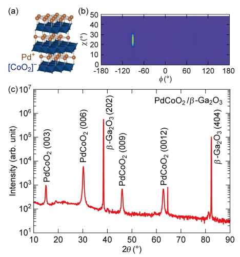
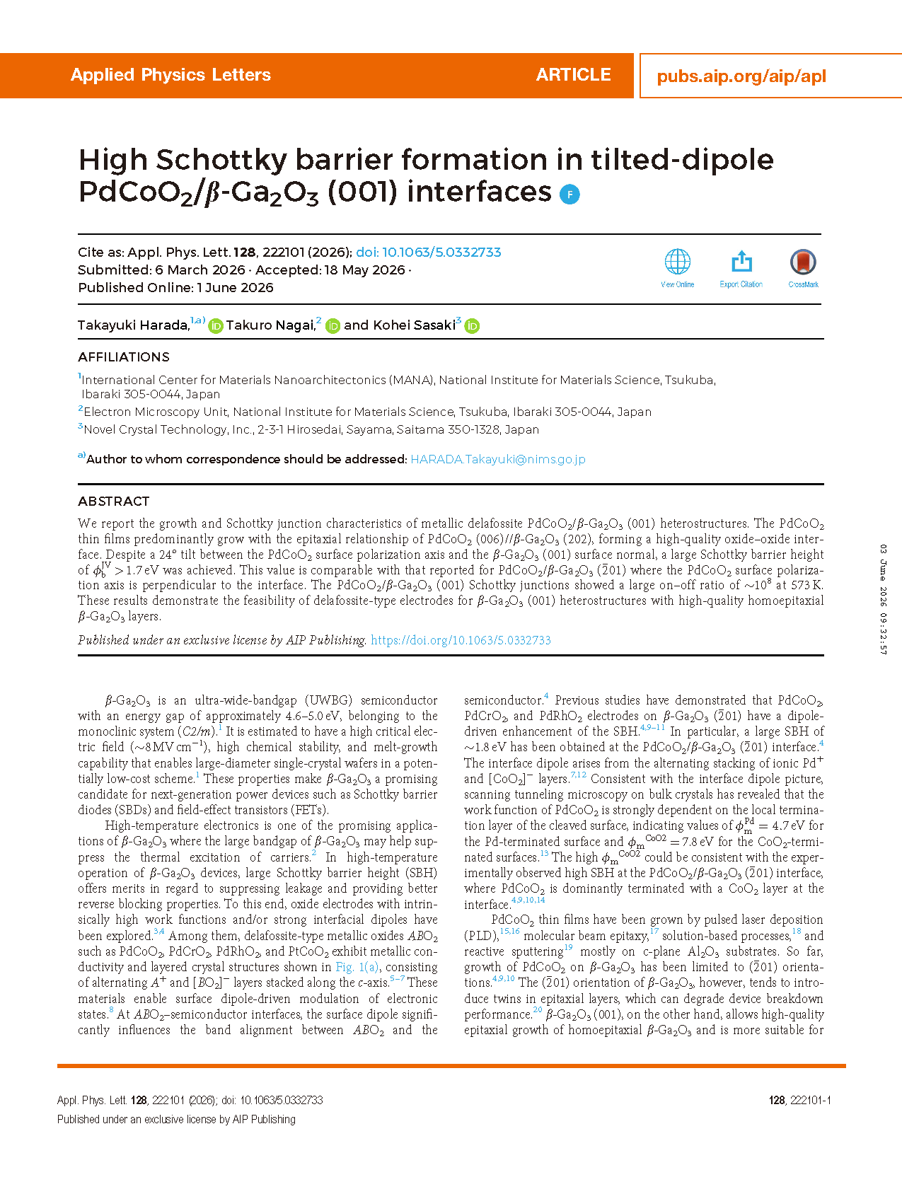
FIG. 1. (a) Crystal structure of PdCoO₂ highlighting the alternating ionic layers of Pd⁺ and [CoO₂]⁻. (b) XRD φ–χ mapping of the PdCoO₂ (006) reflection for PdCoO₂/β-Ga₂O₃ (001). (c) XRD 2θ–w scan of PdCoO₂/β-Ga₂O₃ (001) along the reciprocal vector G003n of PdCoO₂, measured in asymmetric geometry.
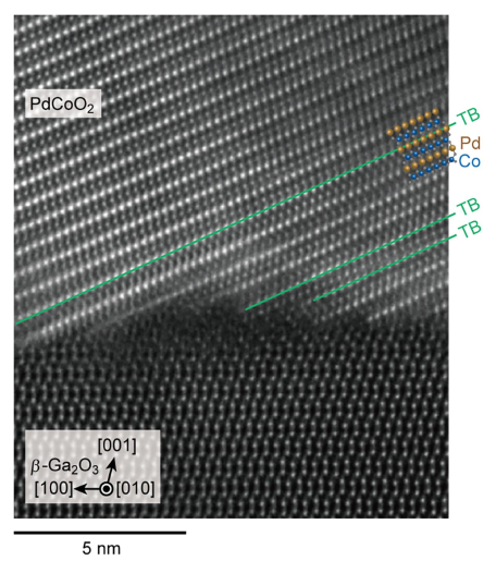
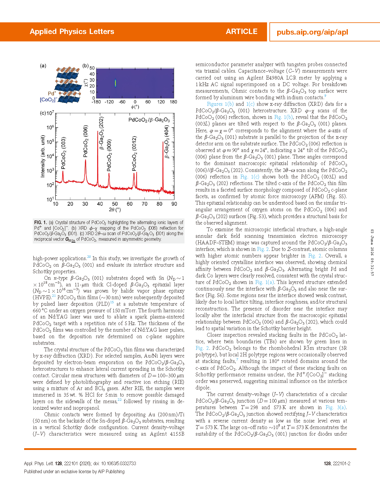
FIG. 2. HAADF–STEM image of a PdCoO₂/β-Ga₂O₃ (001) interface. The crystal model of PdCoO₂ is overlapped in the HAADF–STEM image. Twin boundaries (TBs) in the stacking faults are indicated by green lines.
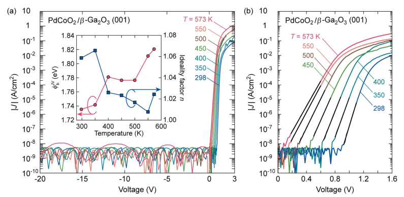
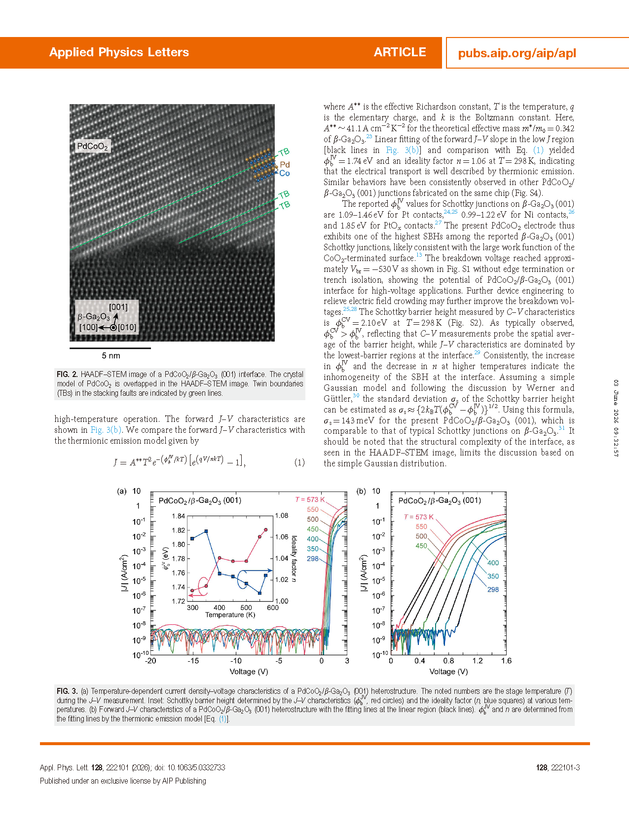
FIG. 3. (a) Temperature-dependent current density–voltage characteristics of a PdCoO₂/β-Ga₂O₃ (001) heterostructure. The noted numbers are the stage temperature (T) during the J–V measurement. Inset: Schottky barrier height determined by the J–V characteristics (φbJV, red circles) and the ideality factor (n, blue squares) at various temperatures. (b) Forward J–V characteristics of a PdCoO₂/β-Ga₂O₃ (001) heterostructure with the fitting lines at the linear region (black lines). φbJV and n are determined from the fitting lines by the thermionic emission model.
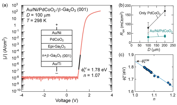
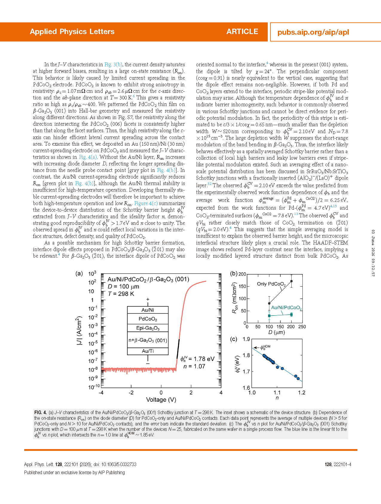
FIG. 4. (a) J–V characteristics of the Au/Ni/PdCoO₂/β-Ga₂O₃ (001) Schottky junction at T = 298 K. The inset shows a schematic of the device structure. (b) Dependence of the on-state resistance (Rₒₙ) on the diode diameter (D) for PdCoO₂-only and Au/Ni/PdCoO₂ contacts. Each data point represents the average of multiple devices (N ≥ 5 for PdCoO₂-only and N≥ 10 for Au/Ni/PdCoO₂ contacts), and the error bars indicate the standard deviation. (c) The φbJV vs n plot for Au/Ni/PdCoO₂/β-Ga₂O₃ (001) Schottky junctions with D=100 μm at T =298 K when the number of the devices N=25, fabricated on the same wafer in a single process flow. The blue line is the linear fit to the φbJV vs n plot, which intersects the n =1.0 line at φbHOM ≈1.85 eV.
DOI:
doi.org/10.1063/5.0332733