Paper Sharing
【Domestic Papers】UWBG Ga₂O₃/AlN DUV Phototransistors on Si Platform for In-sensor Memory and Computing based on Polarization-Induced Carrier Separation
日期:2026-06-11阅读:11
Researchers from University of Science and Technology of China, National University of Defense Technology have published a dissertation titled "UWBG Ga₂O₃/AlN DUV Phototransistors on Si Platform for In-sensor Memory and Computing based on Polarization-Induced Carrier Separation" in 2025 IEEE International Electron Devices Meeting.
Background
Deep ultraviolet photodetection is irreplaceable in flame monitoring, deep-space exploration and environmental ozone detection. Ultra-wide band Ga₂O₃ matches solar-blind spectrum and serves as core candidate for advanced DUV optoelectronics owing to its wide bandgap and high breakdown field. Conventional intelligent optical systems consist of discrete detector, memory and computing chips, which bring complicated layout, high power consumption and large signal delay and fail to satisfy miniaturization demand. Most existing Ga₂O₃-based devices are single-functional for detection or short-term synaptic calculation without integrated long-term nonvolatile memory. Few heterojunction devices adopt interfacial polarization to regulate dual storage characteristics and realize Si-compatible manufacturing, leaving a critical research gap for all-in-one optoelectronic chips.
Abstract
Integration of sensing, memory, and computing in one unit on commercial platform caters to future development of intelligent photodetection systems. Here, ultra-wide bandgap (UWBG) Ga₂O₃/AlN/Si transistor (GAST) with high deep-ultraviolet (DUV) responsivity (275 A/W) is developed for both in-sensor memory and computing. Polarization in Al-polar AlN contributes to both depletion of the Ga₂O₃ channel and non-volatile trapping of holes at the Ga₂O₃/AlN interface. Such effects endow the GAST with ultra-low leakage current (0.26 pA) and long-term multilevel storage. The GAST also harvests short-term memory for synapse-like computing as a reservoir based on tunable persistent photoconductivity (PPC) dominated by Ga₂O₃ bulk traps. Physical reservoir computing (PRC) system, constructed with such all-in-one GAST devices, achieves a 96.75% accuracy in motion direction recognition. This work demonstrates the great potential of UWBG transistors with polarization effect on mature Si platform for advanced in-sensor memory and computing application.
Highlights
For the first time, AlN interface polarization induced carrier separation is adopted to fabricate all-in-one Ga₂O₃/AlN DUV phototransistor with detection, long-term memory and short-term synaptic functions on Si substrate
Nonvolatile multilevel storage is realized via interfacial hole trapping, and tunable short-term synaptic behavior originates from PPC effect of bulk traps inside Ga₂O₃
The device obtains ultra-low leakage current of 0.26 pA and high DUV responsivity of 275 A/W with ~10 V memory window
Reservoir computing system constructed by the devices achieves 96.75% accuracy for motion direction identification
Conclusion
We tailored high-responsivity (275 A/W) GAST devices for in-sensor memory and computing based on polarizationinduced carrier separation strategy. Compared with reported insensor memory or computing devices (Table 1), the GAST features all-in-one multifunction, low leakage current (0.26 pA), and potential integration application based on mature Si platform. The constructed GAST PRC system achieves a 96.75% accuracy in motion direction recognition. This work demonstrates the great potential of UWBG semiconductor transistors with polarization effect for intelligent in-sensor memory and computing application.
Project Support
This work was partially carried out at Center for Micro and Nanoscale Research and Fabrication of USTC and supported by National Key R&D Program of China (2024YFA1208800).
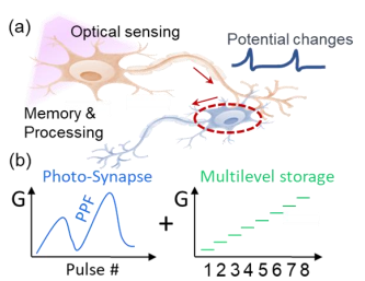
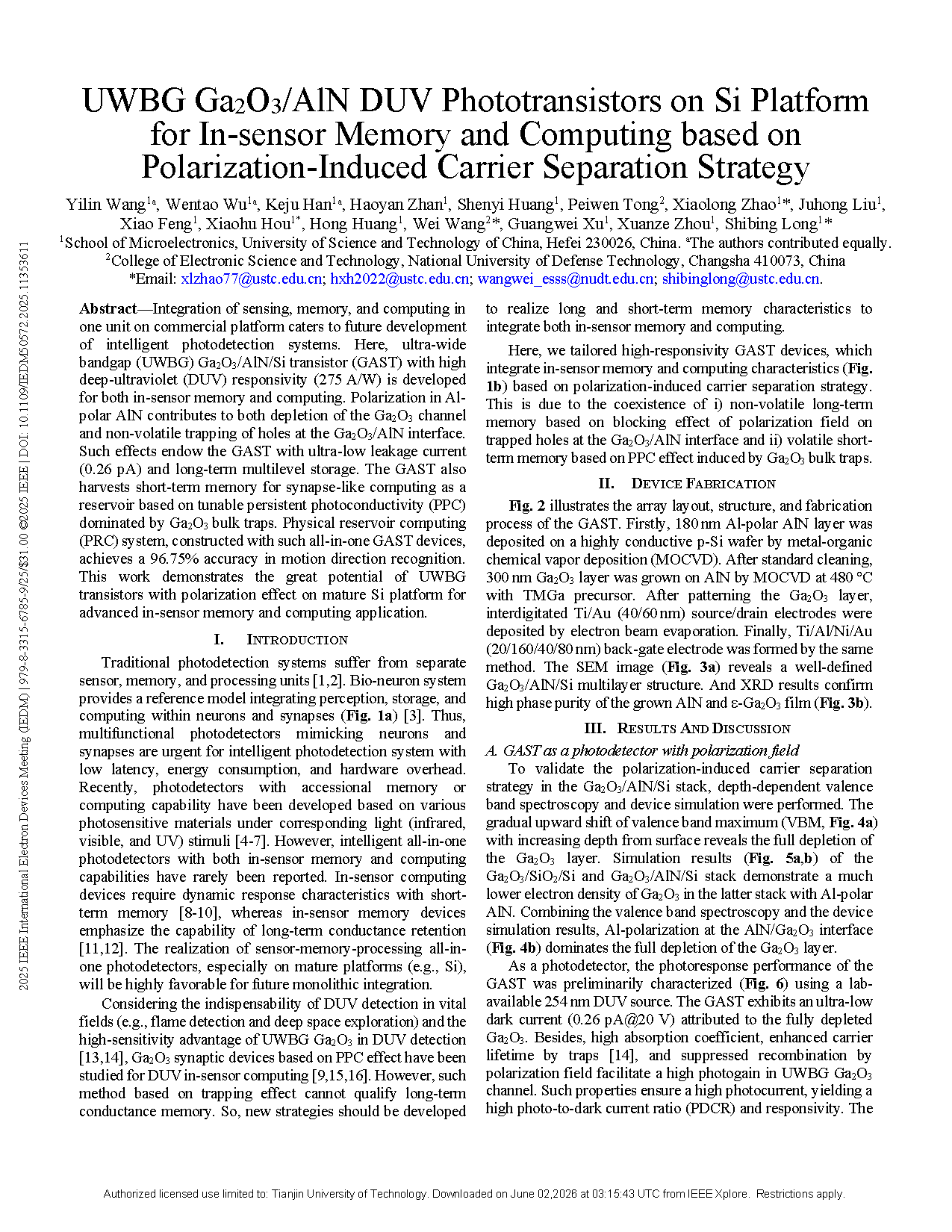
Fig. 1 (a) Synapse-connected neurons in a bio-neuron system with integrated sensing, processing, and memory capability. (b) Synaptic PPF arising from short-term memory and multilevel long-term storage of the GAST, enabling effective emulation of bio-neuronal functions.
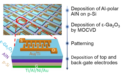
Fig. 2 Schematic of the tailored GAST array and device structure on Si platform. Ga₂O₃ acts as the photosensitive layer, and the Al-polar AlN as the dielectric layer. The fabrication process is shown on the right side of the figure.
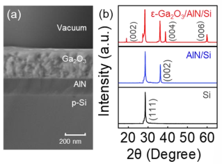
Fig. 3 (a) The cross-sectional SEM image and (b) XRD patterns of each layer in the Ga₂O₃/AlN/Si stack. The results show that (001) ε-Ga₂O₃ and (001) AlN films have been grown on (111) Si substrate with high phase purity.
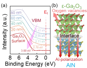
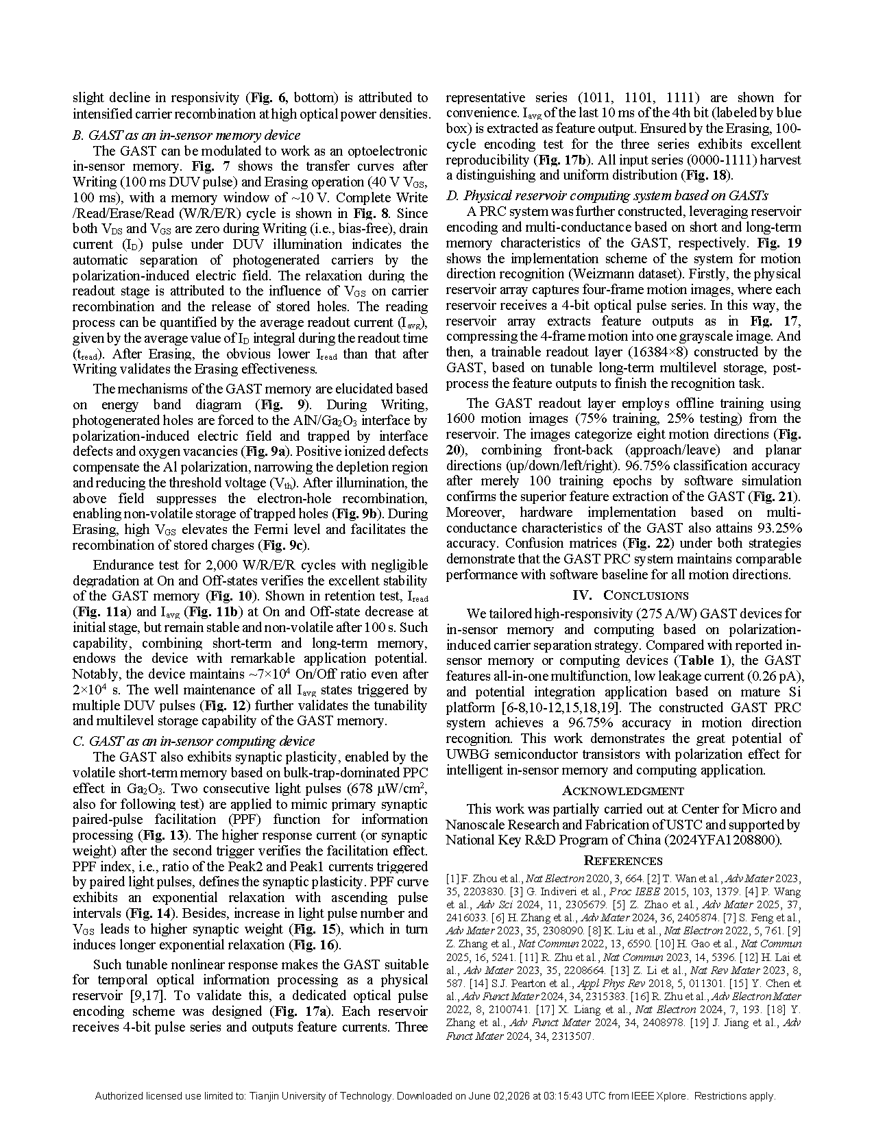
Fig. 4 (a) Depth-resolved valence band spectra of ε-Ga₂O₃ on AlN/Si stack with gradual upward shift of VBM with increasing depth from the surface. (b) Al-polarization direction at the Ga₂O₃/AlN interface. Rich vacancies as typical hole traps in Ga₂O₃ film are also labeled.
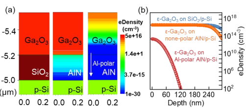
Fig. 5 (a) Electron density distribution simulated by Sentaurus of Ga₂O₃/SiO₂/Si and Ga₂O₃/AlN/Si structures without and with Al polar. (b) Comparison of the depth-dependent electron density in the three structures.The Ga₂O₃ layer on Al-polar AlN/Si stack presents much lower electron density, indicating the strong depletion effect of the Al-polar AlN on the Ga₂O₃ layer.
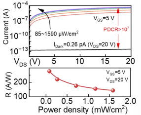
Fig. 6 Typical DUV photoresponse curves of the GAST device (top) and corresponding responsivity (bottom) at various optical power densities. The responsivity ranges from 275 to 140 A/W for the given optical power densities.
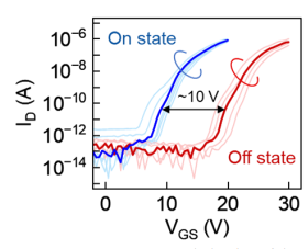
Fig. 7 In-sensor memory behavior of the GAST device. Transfer curves of such GAST memory at On and Off-state exhibit a memory window of ~10 V. The memory window is defined by the difference of Vth.
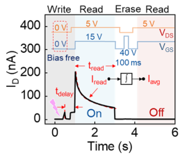
Fig. 8 The ID profiles of a complete W/R/E/R cycle with corresponding electrical schemes labeled at top. The detected positive ID pulse during bias-free Writing under DUV illumination denotes the existence of a built-in electric field.
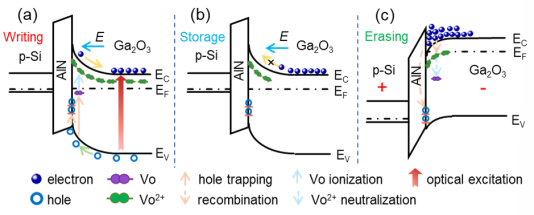
Fig. 9 Schematic energy band diagrams and carrier dynamics of the GAST memory at different stages. (a) Photogenerated carriers are separated by polarization-induced electric field, while holes are trapped during bias-free Writing. (b) The built-in field suppresses recombination of electrons and trapped holes, enabling charge storage. (c) A high VGS pulse during Erasing operation induces electron accumulation, thus promoting the recombination of carriers.
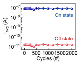
Fig. 10 Endurance performance of the GAST memory with stable Iavg at both On and Off-state for 2000 W/R/E/R cycles, indicating a high operation reliability.
DOI:
doi.org/10.1109/IEDM50572.2025.11353611