Paper Sharing
【Member Papers】Modulation of Microstructural Evolution and Defect States in MOCVD-Grown κ-Ga₂O₃ thin films via In Situ Annealing
日期:2026-06-12阅读:85
Researchers from the Nanjing University of Posts and Telecommunications and Inner Mongolia University have published a dissertation titled " Modulation of Microstructural Evolution and Defect States in MOCVD-Grown κ-Ga2O3 thin films via In Situ Annealing " in Chinese Physics B.
Background
Gallium oxide (Ga₂O₃) is an ultra-wide bandgap semiconductor with a bandgap of 4.8 eV and a high breakdown field of 8 MV/cm, which has broad application prospects in high-power, high-frequency and deep ultraviolet optoelectronic devices. Ga₂O₃ has five polymorphs including α, β, γ, δ and κ (ε), expanding its application range in semiconductor devices. The orthorhombic κ-Ga₂O₃ has low structural anisotropy and no inversion symmetry, thus possessing ferroelectric and piezoelectric properties. Its spontaneous polarization is about 0.23 C/m², nearly one order of magnitude higher than that of GaN, making it a promising material for high electron mobility transistors and two-dimensional electron gas devices.
As a metastable phase, κ-Ga₂O₃ can only be stabilized under kinetically limited growth conditions. When grown by metal-organic chemical vapor deposition (MOCVD), low temperature and low Ⅵ/Ⅲ ratio are required, which are quite different from the growth parameters of thermodynamically stable β-Ga₂O₃. These conditions restrict atomic migration and lattice rearrangement, leading to serious structural disorder and high-density native defects, mainly oxygen vacancies (VO). These defects damage crystal integrity, introduce localized states in the bandgap, and degrade carrier transport and optical properties.
In-situ annealing has been proved to be an effective method to solve the above problems. Previous studies have verified that annealing can remove surface impurities and optimize optical properties of β-Ga₂O₃. However, the relationship among annealing treatment, microstructural evolution and defect states of κ-Ga₂O₃ is still unclear. It has been reported that κ-Ga₂O₃ can maintain phase purity below 700 ℃, which supports the annealing research of this material. In this work, κ-Ga₂O₃ thin films were prepared by MOCVD and treated by in-situ annealing. The effects of annealing on structural quality, surface morphology, chemical states and defect-related luminescence of κ-Ga₂O₃ films were systematically investigated to reveal the kinetic mechanism of defect healing and formation during thermal treatment.
Abstract
Orthorhombic κ-Ga₂O₃ holds immense promise for electronic and optoelectronic devices due to its significant spontaneous polarization and reduced structural anisotropy. However, the kinetically limited growth conditions required to stabilize this metastable phase often led to severe structural disorder and a high density of native defects, primarily oxygen vacancies (VO), which degrade both crystalline integrity and carrier transport properties. In this work, we systematically investigate the modulation of microstructural evolution and defect kinetics in MOCVD-grown κ-Ga₂O₃ films through in situ oxygen-rich annealing. A critical thermal-processing window was identified at 700 °C: an optimized 20-minute treatment significantly enhances structural coherence, yielding a narrow XRD FWHM of 0.74° and a smooth surface with 2.88 nm roughness. XPS and photoluminescence spectra reveal that precise thermal modulation facilitates atomic rearrangement and heals VO, effectively suppressing deep-level donor-acceptor pair recombination. Conversely, excessive annealing (40 min) triggers lattice oxygen loss, leading to VO regeneration and structural degradation. By elucidating the competitive mechanism between defect annihilation and formation, this study provides a strategic pathway for stabilizing the κ-phase and tailoring the optoelectronic properties of Ga₂O₃ based devices.
Highlights
A critical annealing temperature of 700 °C and the optimal annealing time of 20 min are determined for in-situ oxygen-rich treatment of MOCVD-grown κ-Ga₂O₃ thin films.
Moderate annealing effectively improves crystallinity and surface quality, with the XRD FWHM reduced to 0.74° and surface roughness decreased to 2.88 nm.
The competitive mechanism between oxygen vacancy annihilation and regeneration during annealing is revealed for the first time.
Excessive annealing causes lattice oxygen loss and the regeneration of oxygen vacancies, leading to structural and performance degradation of κ-Ga₂O₃ films.
This work provides an effective strategy to stabilize metastable κ-phase Ga₂O₃ and regulate its defect states for optoelectronic device applications.
Conclusion
In conclusion, κ-Ga₂O₃ thin films were fabricated and in situ annealing was performed. The modulation of annealing on the morphological properties and defect related states of κ-Ga₂O₃ films was systematically investigated. The results showed that intrinsic defect states were readily introduced during film growth (S1). Under high-temperature and oxygen-rich conditions, an appropriate annealing process effectively repaired defect states in κ-Ga₂O₃ (S2), leading to improved crystal quality with a FWHM of 0.74°. SEM and AFM observations further revealed that the film surface became denser and smoother, with the surface roughness reduced to 2.88 nm. XPS analysis indicated that the VO concentration decreased to as low as 7.4%, while the PL spectroscopy further confirmed the reduction in defect concentration. In contrast, excessive annealing deteriorates the film properties (S3). Based on band-structure considerations, the origin and evolution of defect states in κ-Ga₂O₃ are clarified, confirming that the decrease in defect concentration after appropriate annealing is mainly associated with the repair of oxygen vacancies, whereas the increased defect concentration after excessive annealing primarily originates from additional oxygen vacancies formed by oxygen loss from the lattice. These findings highlight that in situ annealing is an effective approach for stabilizing the metastable κ-Ga₂O₃ phase and regulating its defect states, thereby providing important guidance for further tailoring its material properties and designing related devices.
Project Support
This work was funded by the National Natural Science Foundation of China (62305171 and U23A20349), the Basic Research Program of Jiangsu (BK20253003), the Suzhou Critical Core Technology Research Project (SYG2024003), the Natural Science Foundation of Jiangsu Province (BK20230361), the Young Scientific and Technological Talents Promotion Project of Jiangsu Province (JSTJ-2024-197), the Jiangsu Provincial Team of Innovation and Entrepreneurship (JSSCTD202351), Postgraduate Research & Practice Innovation Program of Jiangsu Province
(KYCX25_1140).
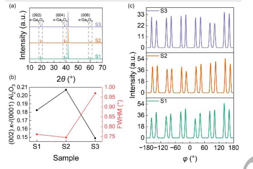
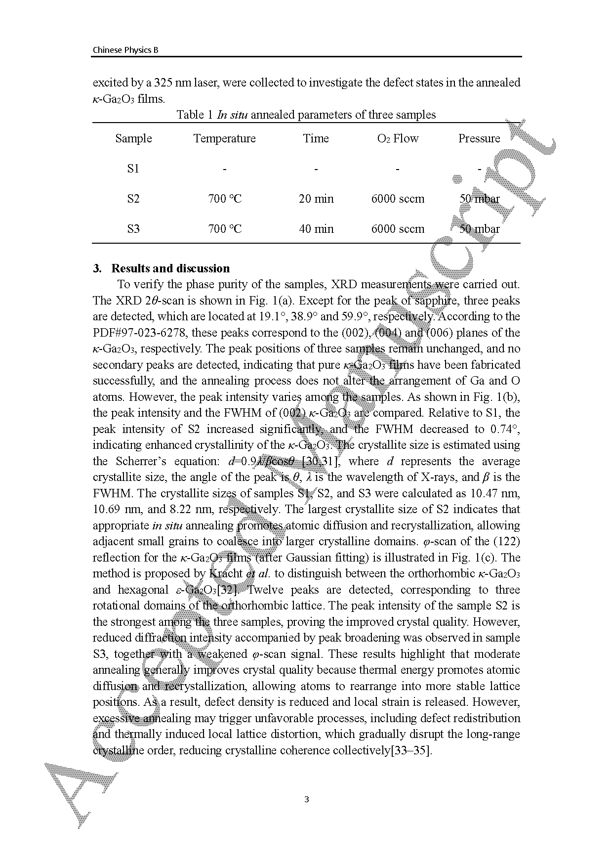
Fig. 1. (a) XRD 2θ-scan of S1, S2 and S3; (b) The XRD peak intensity ratio of (002) κ-Ga₂O₃/(0001) Al₂O₃ and FWHM of (002) κ-Ga₂O₃; (c) XRD φ-scan of (122) plane reflection on κ-Ga₂O₃ films after Gaussian fitting.
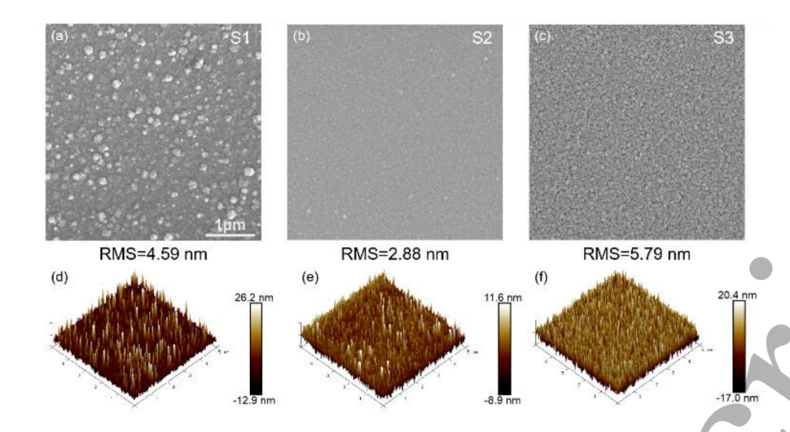
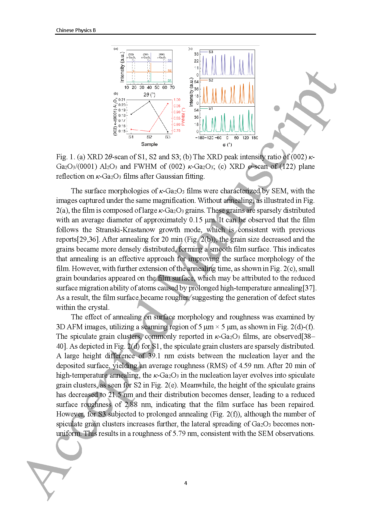
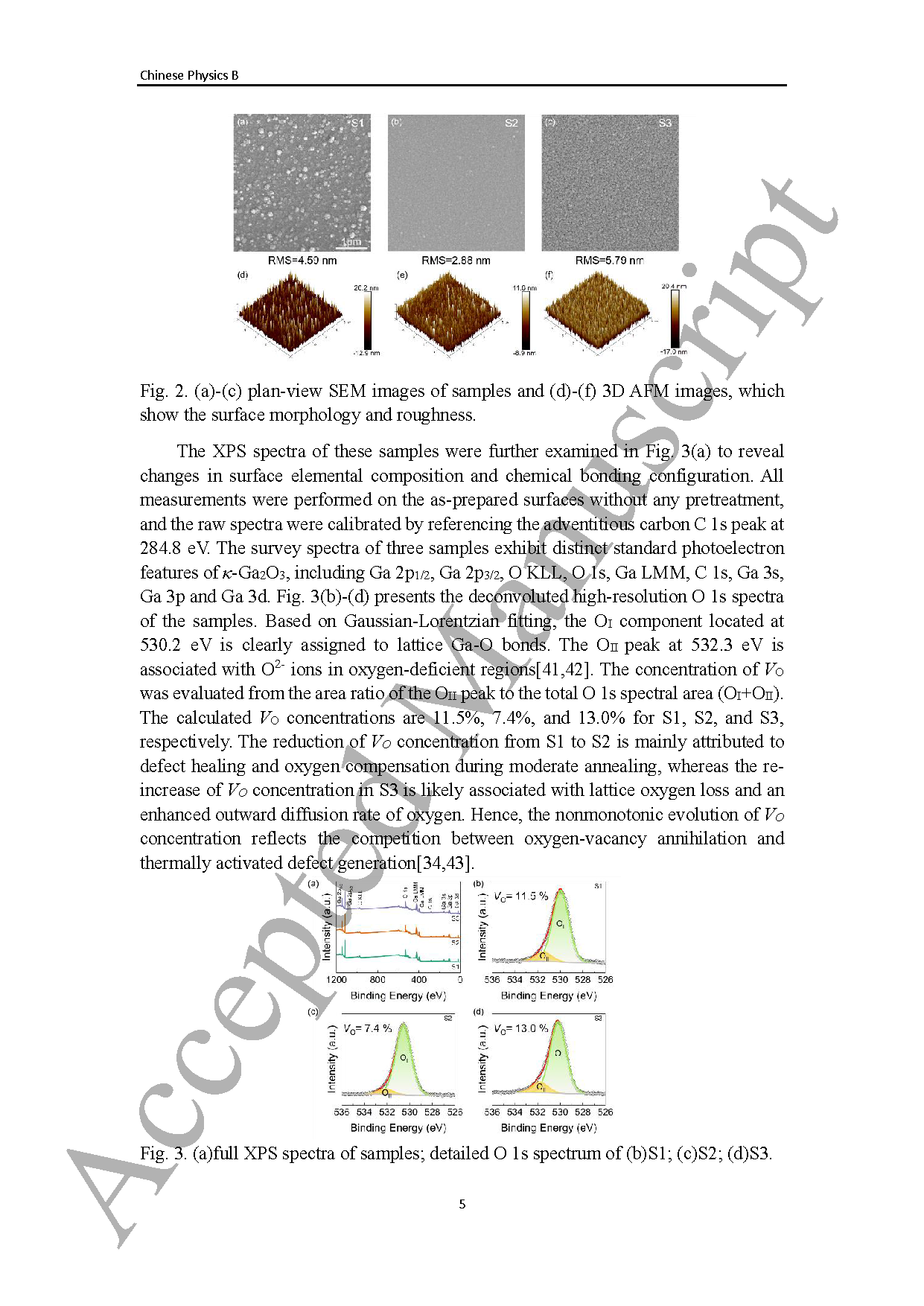
Fig. 2. (a)-(c) plan-view SEM images of samples and (d)-(f) 3D AFM images, which show the surface morphology and roughness.
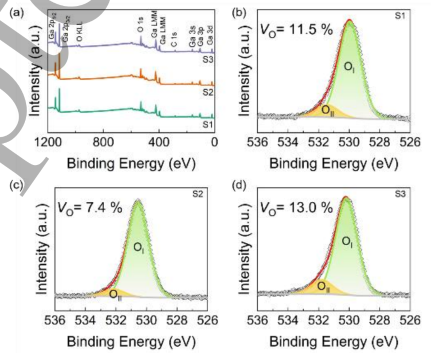
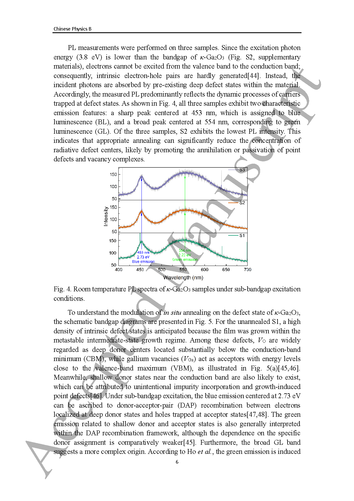
Fig. 3. (a) full XPS spectra of samples; detailed O 1s spectrum of (b) S1; (c) S2; (d) S3.
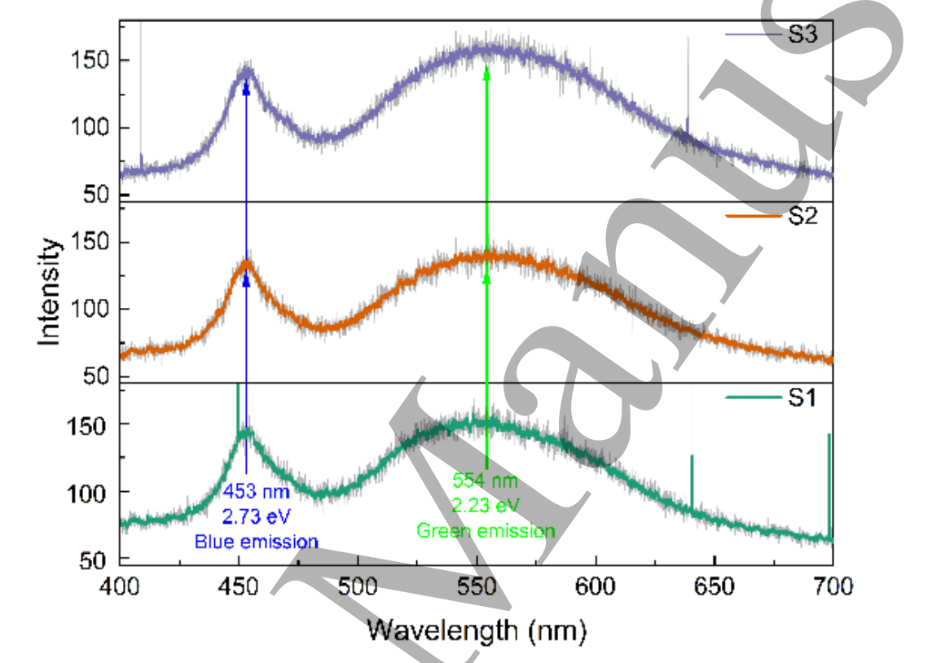
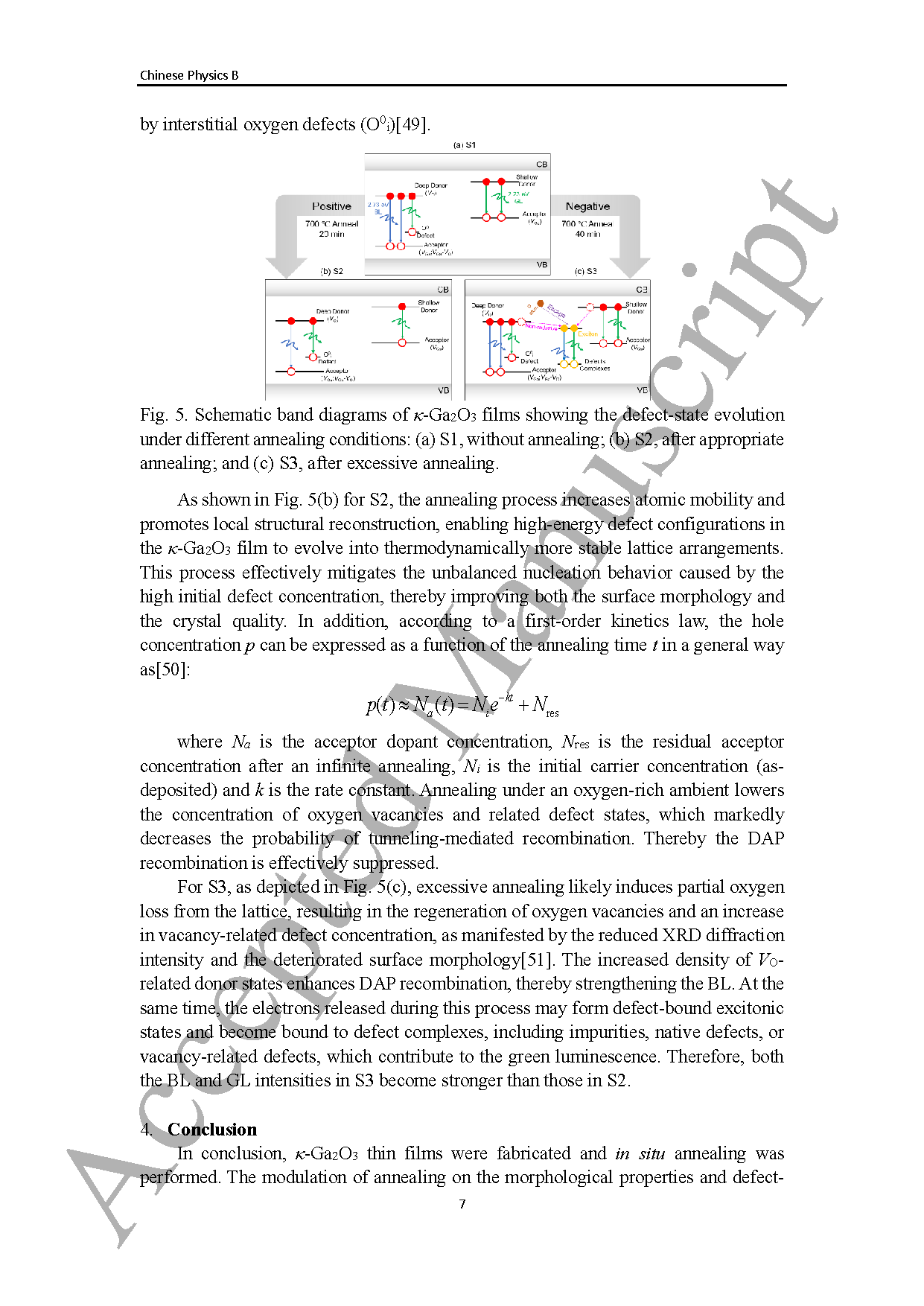
Fig. 4. Room temperature PL spectra of κ-Ga₂O₃ samples under sub-bandgap excitation conditions.
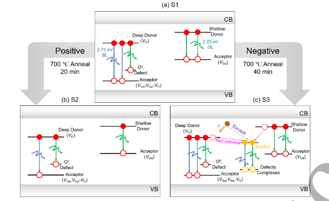
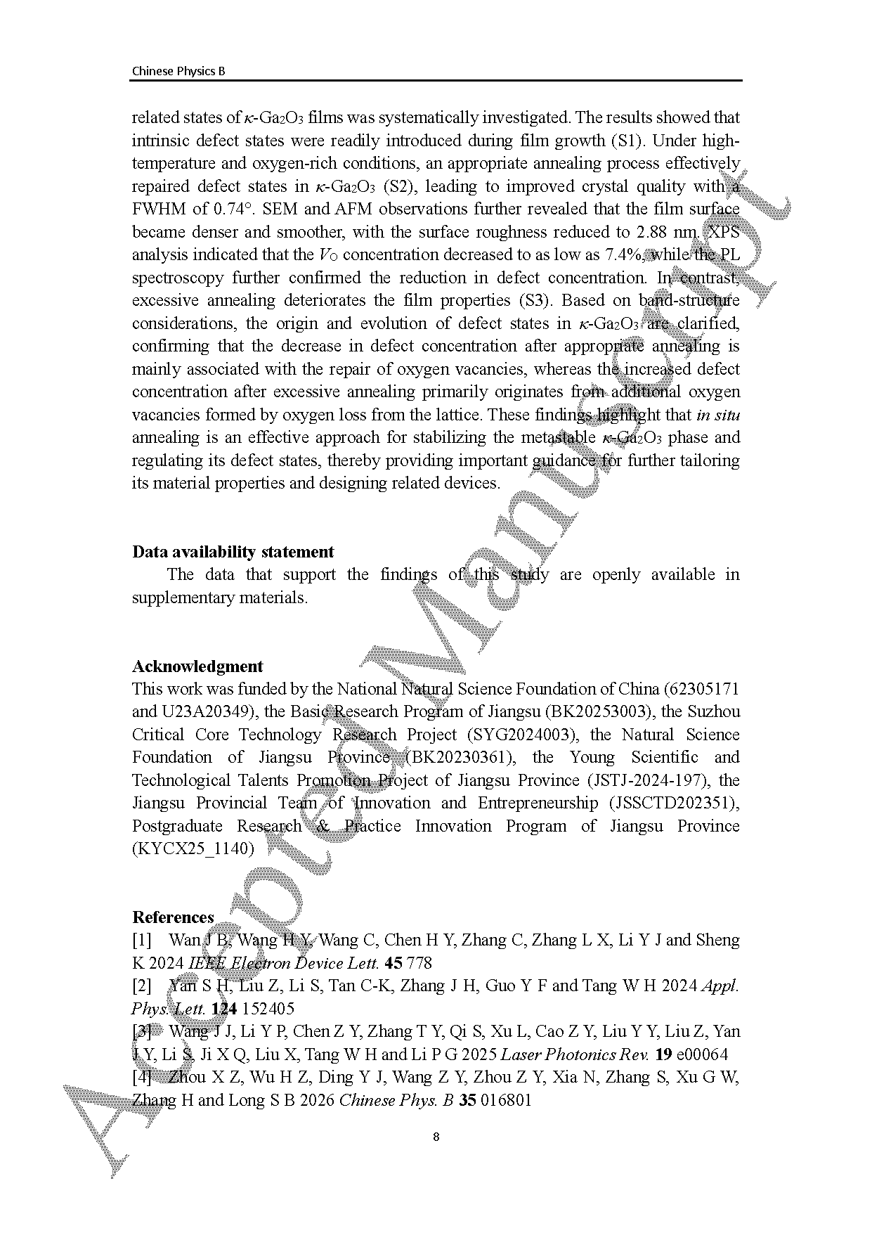
Fig. 5. Schematic band diagrams of κ-Ga₂O₃ films showing the defect-state evolution under different annealing conditions: (a) S1, without annealing; (b) S2,after appropriate annealing; and (c) S3, after excessive annealing.
DOI :
10.1088/1674-1056/ae77d2