Paper Sharing
【International Papers】Intrinsic Thermal Instability of δ-Ga₂O₃ Thin Films Grown via Mist Chemical Vapor Deposition
日期:2026-06-15阅读:53
Researchers from Kyoto Institute of Technology have published a dissertation titled " Intrinsic Thermal Instability of δ-Ga₂O₃ Thin Films Grown via Mist Chemical Vapor Deposition " in Crystal Growth & Design.
Background
Ultrawide-bandgap (4.6−5.3 eV) gallium oxide (Ga₂O₃) has attracted significant attention as a promising material for high power and high-voltage device applications owing to its high breakdown electric field. Ga₂O₃ possesses five crystal polymorphs: α, β, γ, δ, and κ(ε). Among these polymorphs, the β-phase is the most thermodynamically stable, and bulk substrates can be grown via melting methods. Consequently, homoepitaxial growth is feasible, and most research on Ga₂O₃ has focused on the β-phase.
Abstract
This study demonstrates that δ-Ga₂O₃ thin films grown by mist chemical vapor deposition (CVD) are intrinsically thermally unstable, and that rapid postgrowth cooling is essential to stabilize the δ phase. δ-Ga₂O₃ thin films were deposited on YSZ(111) substrates using a β-Fe₂O₃ buffer layer, and their thermal stability was systematically investigated. X-ray diffraction (XRD) showed that δ-Ga₂O₃ is stabilized only within a narrow growth-temperature window of 550−625 °C. Postgrowth annealing caused the disappearance of δ-Ga₂O₃ diffraction peaks at temperatures as low as 500 °C, indicating thermal instability below the growth temperature. Photoluminescence excitation (PLE) spectroscopy probed structural changes beyond the XRD detection limit. The PLE peak shifted from 4.94 eV in as-grown films to 5.12 eV after annealing at 700 °C, consistent with a δ→γ phase transformation, and further to 5.07 eV after annealing at 900 °C, suggesting mixed γ/β phases. The absence of additional diffraction peaks is attributed to nanocrystalline γ or γ/β phases below XRD detectability. δ-Ga₂O₃ also loses crystallinity when held at the growth temperature for more than 10 min, emphasizing the critical role of immediate cooling. These findings provide fundamental insight into δ-Ga₂O₃ metastability and define key processing constraints for its device applications.
Conclusion
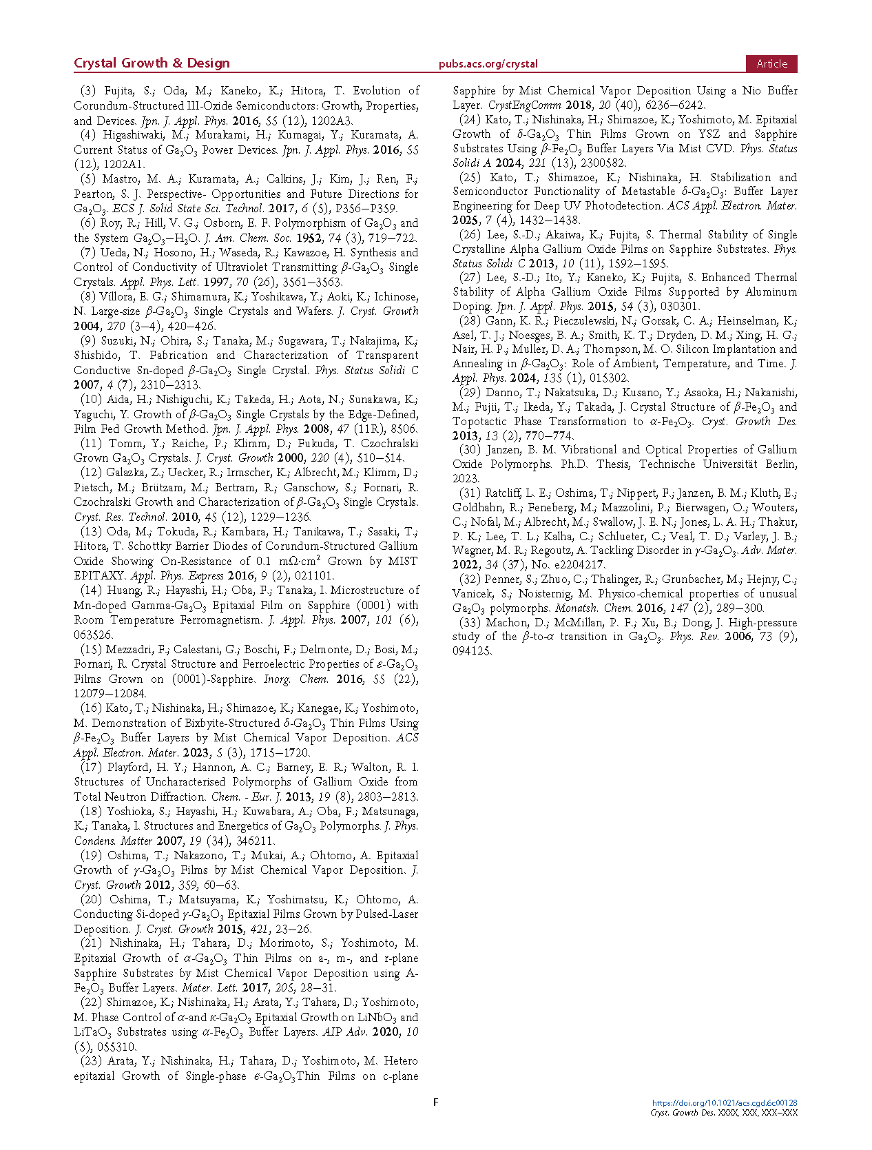
In this study, we systematically investigated the growth temperature range and thermal stability of δ-Ga₂O₃ thin films grown via mist CVD. Single-phase δ-Ga₂O₃ was stabilized only within a narrow growth temperature range of 550−625 °C utilizing β-Fe₂O₃ buffer layers, underscoring the highly metastable nature of the δ-phase. Postgrowth annealing experiments revealed that the characteristic δ-Ga₂O₃ diffraction peaks disappeared after annealing at temperatures as low as 500 °C, which is significantly lower than the growth temperature. PLE analysis provided critical insights into structural evolution that could not be derived from conventional XRD measurements. The observed shifts in the PLE peak positions indicate a δ→γ phase transformation at 700 °C, followed by the formation of mixed γ/β-phases at 900 °C. The absence of corresponding diffraction peaks is attributable to the formation of nanocrystalline phases with crystallite sizes below the XRD detection limit, demonstrating the importance of optical spectroscopy for evaluating metastable Ga₂O₃ polymorphs. Raman spectroscopy further supported the structural evolution of the δ-Ga₂O₃ films. The as-grown sample exhibited Raman peaks at 162, 280, 317, 372, 375, and 531 cm⁻¹, which differ from those reported for other Ga₂O₃ polymorphs (α, β, γ, and κ(ε)) and are therefore attributed to δ-Ga₂O₃. After annealing at 700 and 900 °C, additional Raman peaks consistent with those reported for β-Ga₂O₃ appeared, indicating a phase transformation from the δ-phase to the β-phase. Moreover, the increased peak intensities and the appearance of additional weak peaks in the sample annealed at 900 °C suggest that the transformation to the β-phase progresses further with increasing annealing temperature. Furthermore, we demonstrated that δ-Ga₂O₃ rapidly loses its crystallinity when samples are held at the growth temperature for more than 10 min after deposition, highlighting the critical role of the postgrowth cooling process. This behavior indicates that the thermal instability of δ-Ga₂O₃ is intrinsic and not induced by the degradation of the β-Fe₂O₃ buffer layer. Therefore, the ability of mist CVD to enable immediate sample removal and rapid cooling is essential for the realization of δ-Ga₂O₃ thin films. These findings establish fundamental processing constraints for stabilizing δ-Ga₂O₃ and provide important guidelines for the growth and integration of metastable Ga₂O₃ polymorphs in future electronic and optoelectronic device applications.
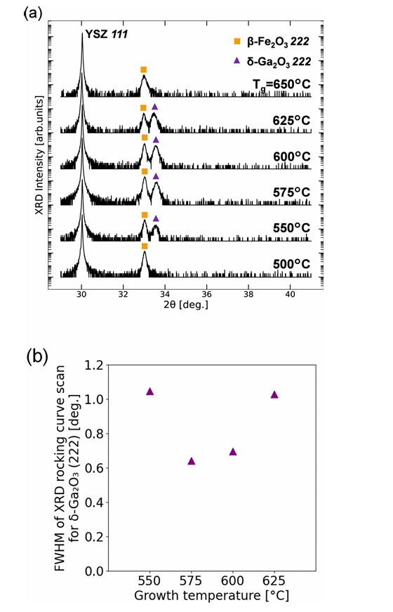
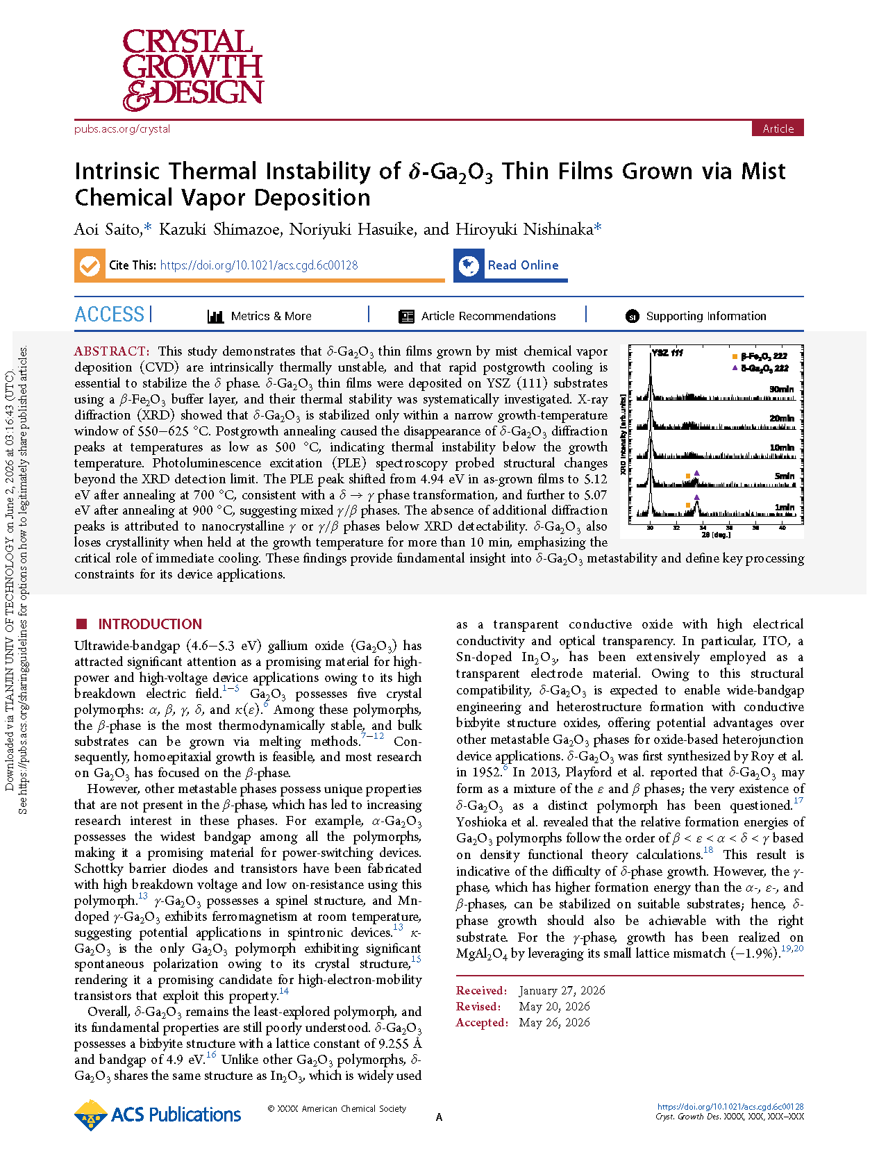
Figure 1. (a) XRD 2θ−ω scan of Ga₂O₃ thin films grown at temperatures ranging from 500 to 650 °C for 10 min; (b) FWHM of the XRD rocking curve scans of the (222) planes of δ-Ga₂O₃ thin films grown at different temperatures.
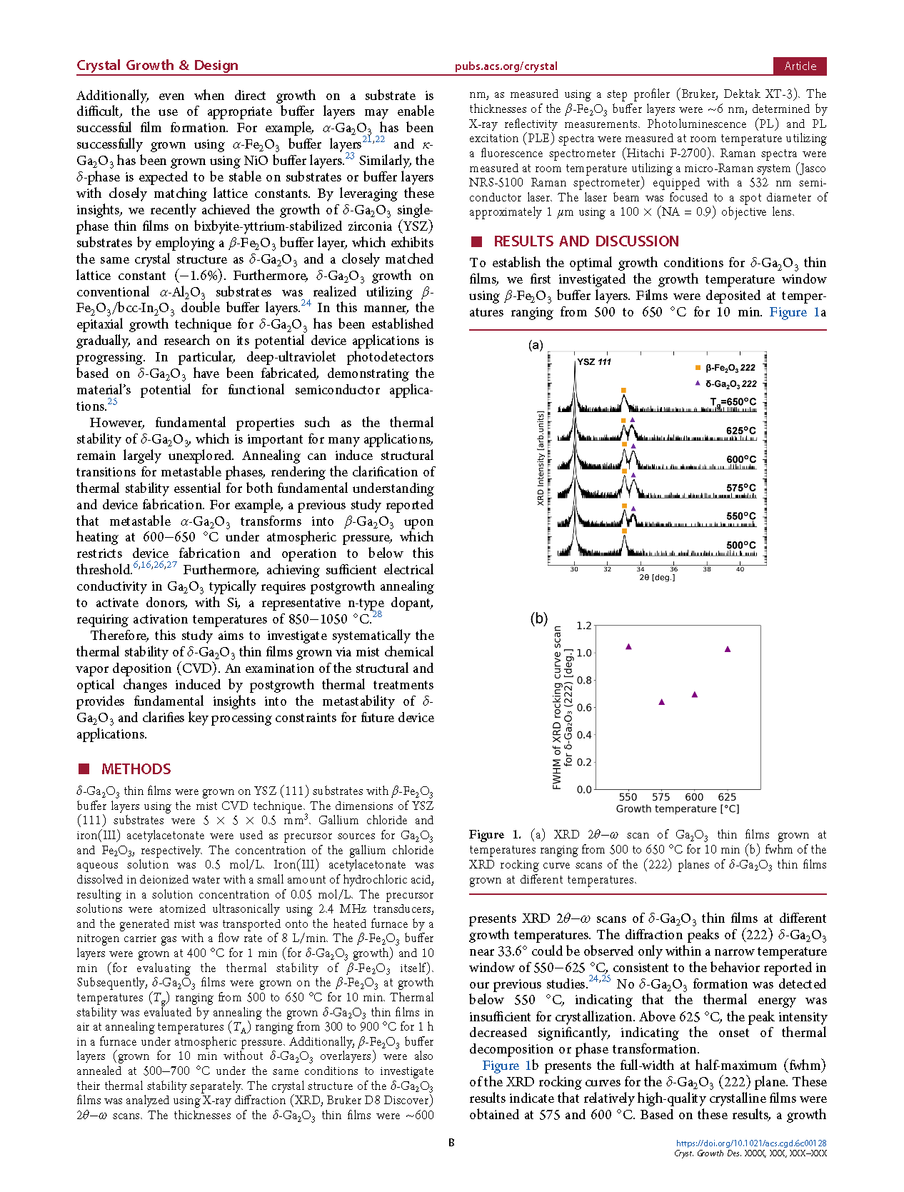
Figure 2. (a) XRD 2θ−ω scans of δ-Ga₂O₃ thin films annealed at temperatures ranging from 300 to 900 °C for 1 h in the 2θ range of 29−41°. (b) Wide-range XRD 2θ−ω scans (10−90°) for δ-Ga₂O₃ thin films annealed at 700 and 900 °C.
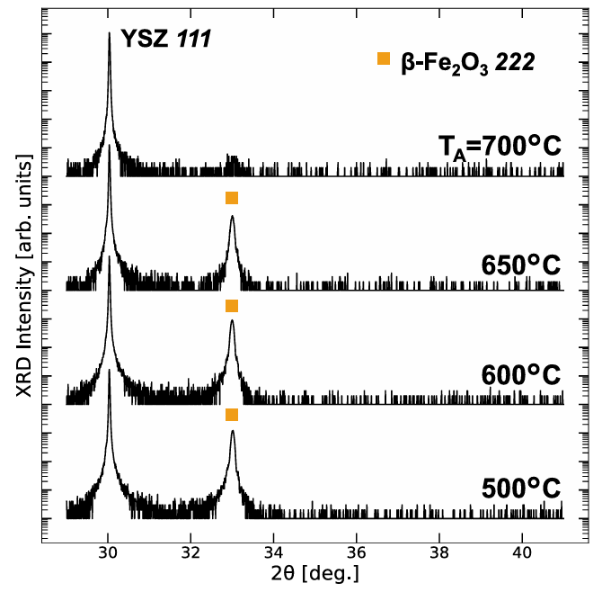
Figure 3. XRD 2θ−ω scans of β-Fe₂O₃ thin films annealed at temperatures ranging from 500 to 700 °C.
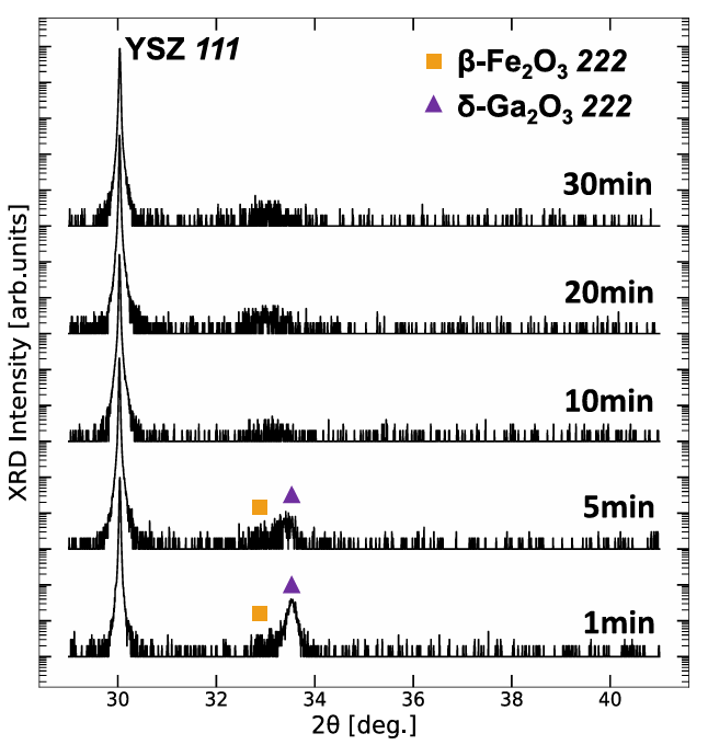
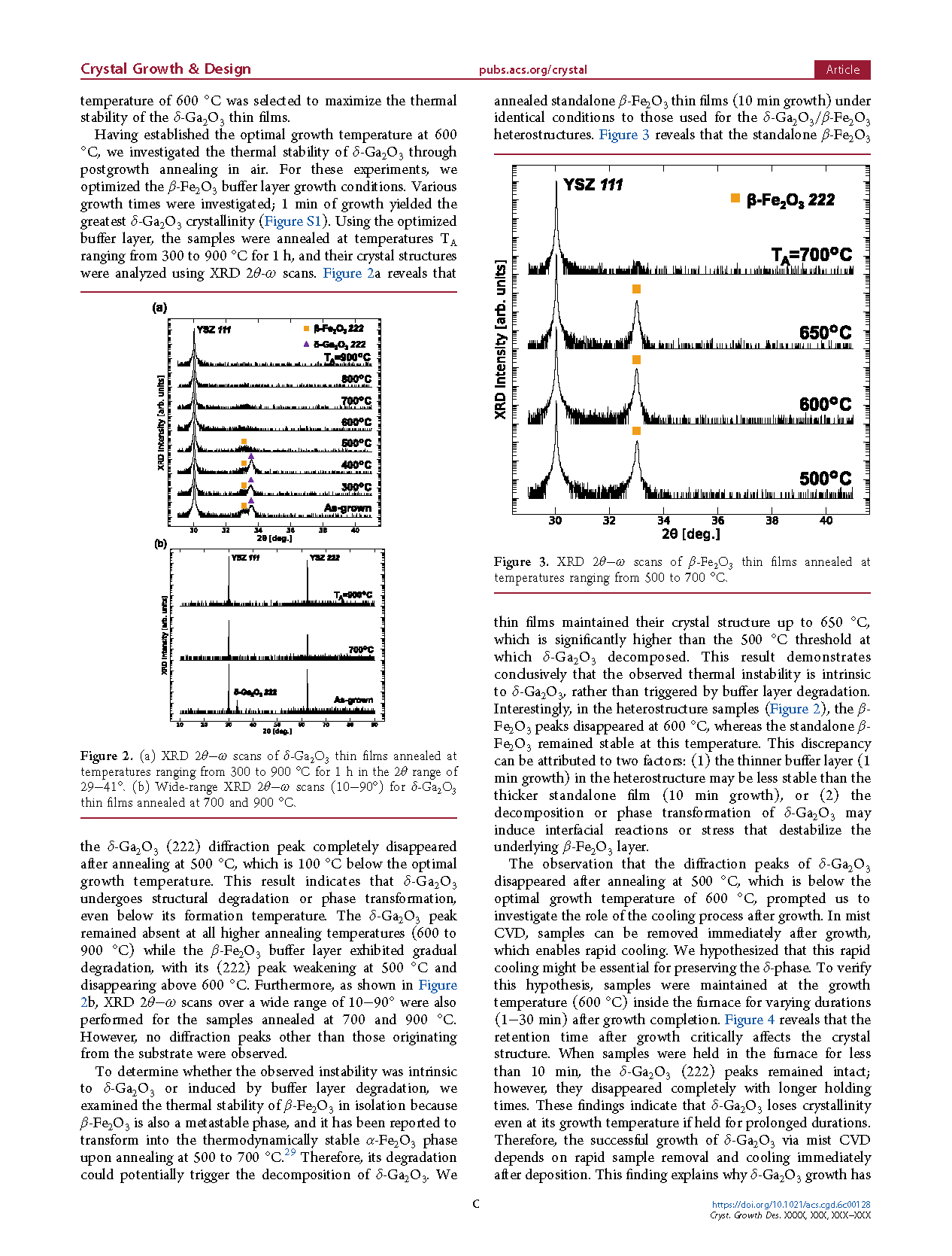
Figure 4. XRD 2θ−ω scans of Ga₂O₃ thin films held in the furnace 1 to 30 min after growth.
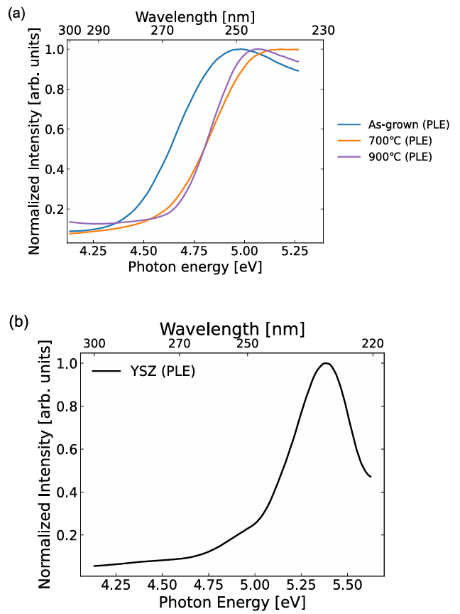
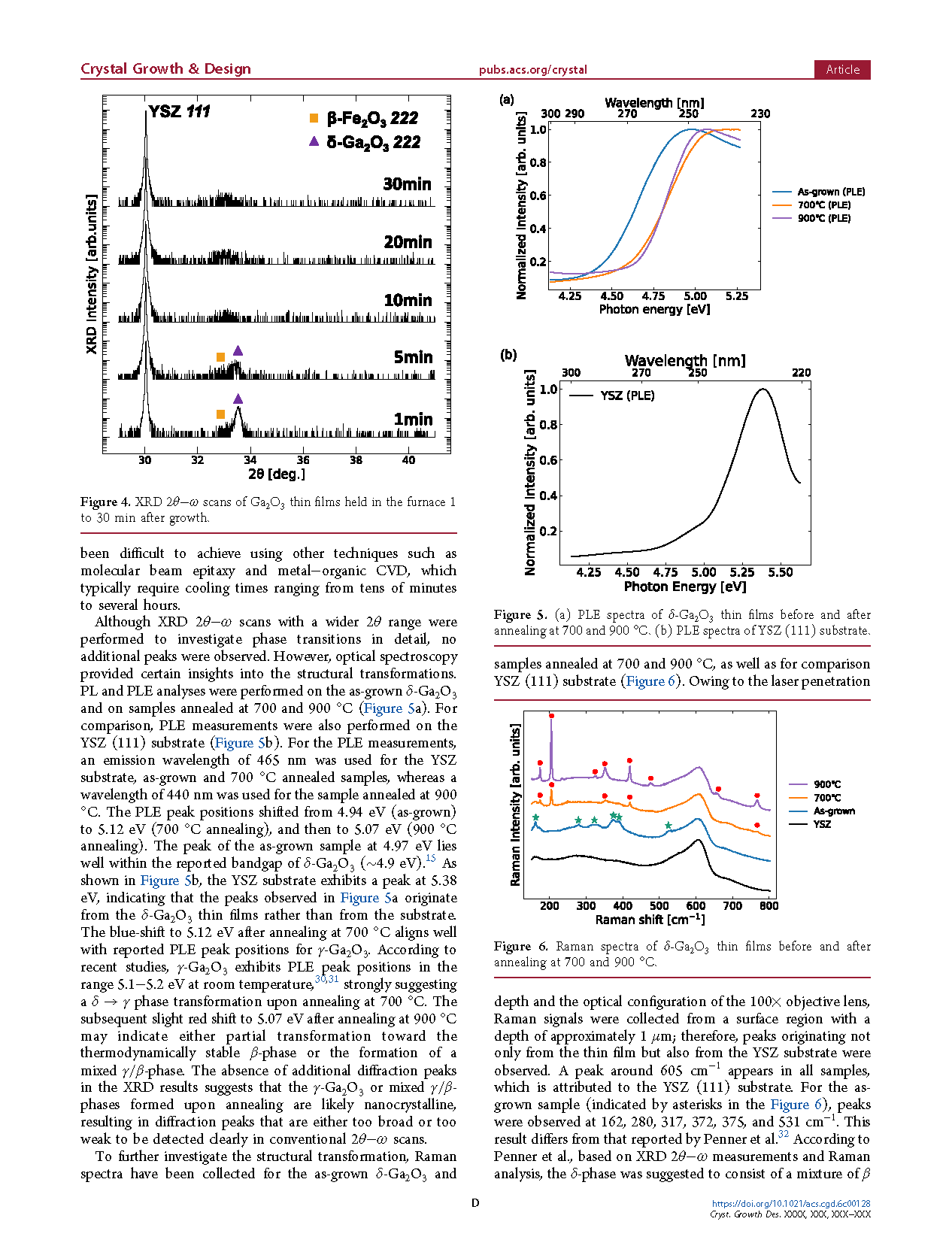
Figure 5. (a) PLE spectra of δ-Ga₂O₃ thin films before and after annealing at 700 and 900 °C. (b) PLE spectra of YSZ (111) substrate.
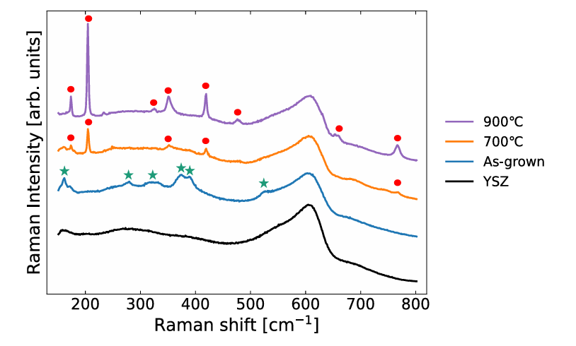
Figure 6. Raman spectra of δ-Ga₂O₃ thin films before and after annealing at 700 and 900 °C.
DOI:
doi.org/10.1021/acs.cgd.6c00128