Paper Sharing
【Member Papers】Electro-Thermal Improvement in a β‑Ga₂O₃ Cage-Integrated Slanted-Fin MOSFET
日期:2026-06-15阅读:57
Researchers from Xidian University have published a dissertation titled “Electro-Thermal Improvement in a β‑Ga₂O₃ Cage-Integrated Slanted-Fin MOSFET” in Micromachines.
Background
β‑Ga₂O₃ is an ideal candidate for next-generation power devices as an ultra-wide bandgap semiconductor with high Baliga’s figure of merit and high critical breakdown electric field. However, its low intrinsic thermal conductivity leads to severe self-heating effect, and serious electric-field crowding in the gate-to-drain region restricts the synergistic improvement of high-voltage capability and heat dissipation. Most existing studies focus on either electric-field modulation or thermal management alone, failing to achieve both breakdown voltage improvement and self-heating suppression in a single device structure. There is a lack of experimentally verified device-layout-level strategy for electro-thermal co-optimization.
Abstract
Electro-thermal improvement is critical for β‑Ga₂O₃ power devices to mitigate self-heating while maintaining high-voltage capability. Here, we propose a β‑Ga₂O₃ cage-integrated slanted-fin MOSFET (C-SFMOSFET). By optimizing the cage-to-fin and cage-to-drain distances, the cage sequence simultaneously strengthens channel depletion and enhances heat dissipation in the gate-to-drain region. Compared with the baseline slanted-fin MOSFET (SFMOSFET), the proposed 4-cage C-SFMOSFET achieves a 1.75× higher Baliga’s figure of merit and reduces the peak junction temperature by 8 °C at 0.55 W/mm. These results indicate that the proposed device layout can effectively improve device-level electro-thermal performance and further exploit the inherent advantages of ultra-wide-bandgap β‑Ga₂O₃.
Highlights
A cage-integrated slanted-fin structure is proposed to realize electro-thermal co-optimization for β‑Ga₂O₃ MOSFETs.
The cage sequence optimizes electric-field distribution and suppresses electric-field crowding in the gate-to-drain region.
The cage structure provides additional heat-spreading paths and enhances topside heat dissipation.
The 4-cage C-SFMOSFET increases BFOM by 1.75× and reduces Tpeak by 8 °C experimentally.
The electro-thermal improvement strategy is validated by both TCAD simulations and experimental measurements.
Conclusion
In summary, an electro-thermally improved β‑Ga₂O₃ C-SFMOSFET is presented in this study. The cage-integrated slanted-fin structure improves channel depletion and raises the breakdown voltage. In addition, the cage sequence promotes thermal transport and topside heat dissipation, which helps improve its high-temperature power handling. Despite the low thermal conductivity of β‑Ga₂O₃, the proposed device-level electro-thermal improvement layout offers a practical balance between thermal constraints and electrical performance, providing useful design guidance for thermally sensitive β‑Ga₂O₃ devices. Future work will extend this framework to the design of large-sized β‑Ga₂O₃ power devices.
Project Support
This work was supported by the National Natural Science Foundation of China (Grant No. 62204187).
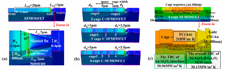
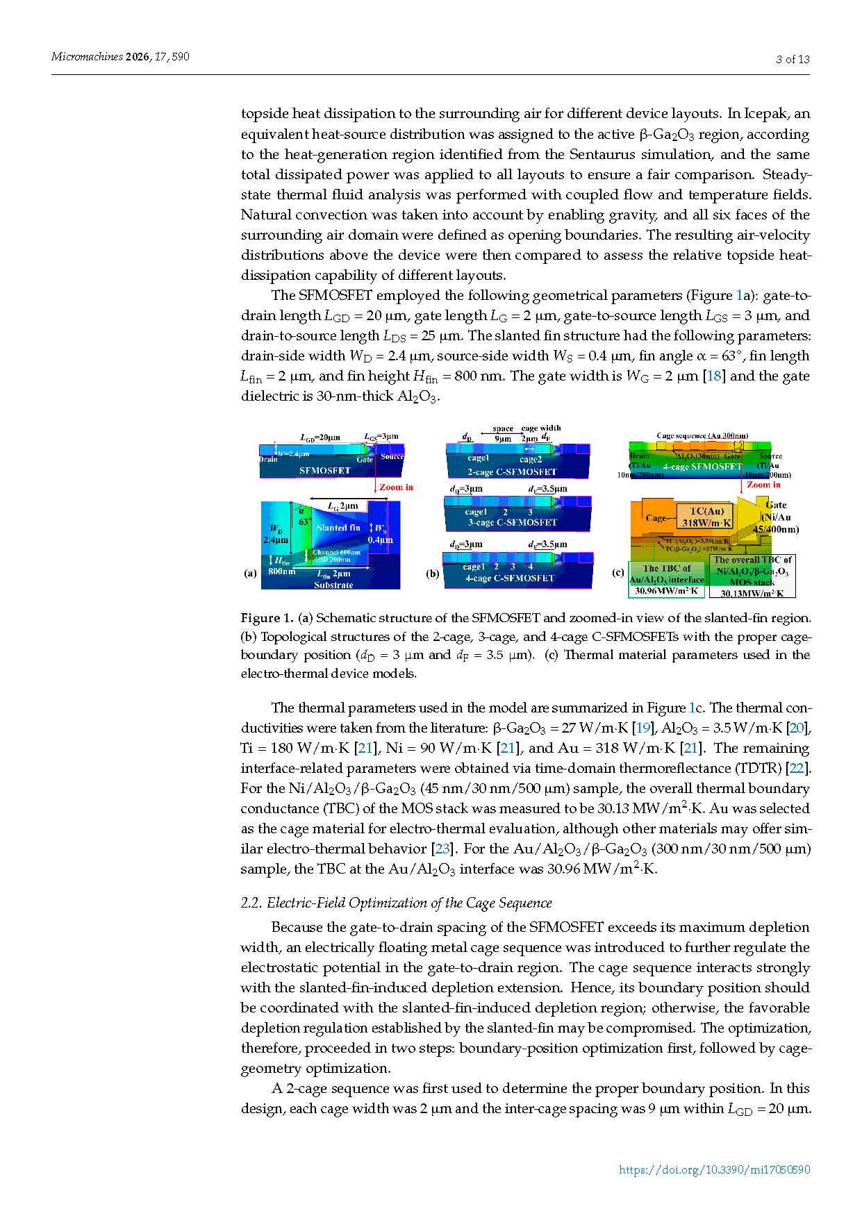
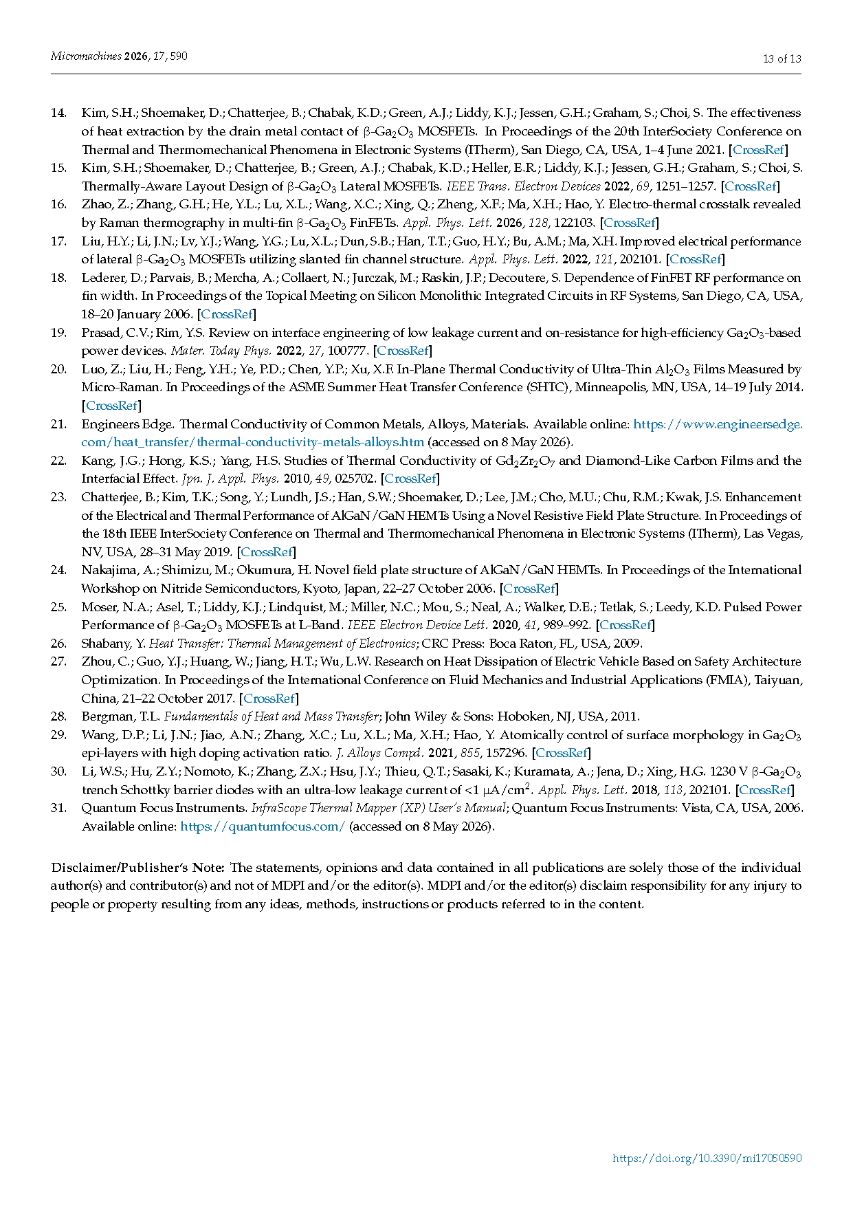
Figure 1. (a) Schematic structure of the SFMOSFET and zoomed-in view of the slanted-fin region. (b) Topological structures of the 2-cage, 3-cage, and 4-cage C-SFMOSFETs with the proper cage boundary position (dD = 3 μm and dF = 3.5 μm). (c) Thermal material parameters used in the electro-thermal device models.
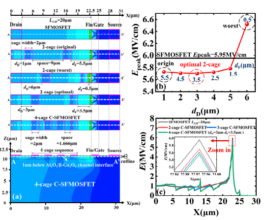
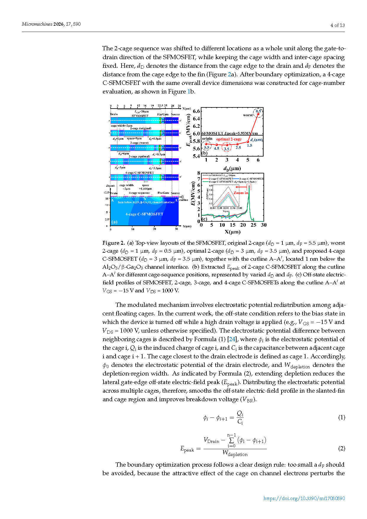
Figure 2. (a) Top-view layouts of the SFMOSFET, original 2-cage (dD = 1 μm, dF = 5.5 μm), worst 2-cage (dD = 1 μm, dF = 0.5 μm), optimal 2-cage (dD = 3 μm, dF = 3.5 μm), and proposed 4-cage C-SFMOSFET (dD = 3 μm, dF = 3.5 μm), together with the cutline A–A′, located 1 nm below the Al₂O₃/β‑Ga₂O₃ channel interface. (b) Extracted Epeak of 2-cage C-SFMOSFET along the cutline A–A′ for different cage-sequence positions, represented by varied dD and dF. (c) Off-state electric-field profiles of SFMOSFET, 2-cage, 3-cage, and 4-cage C-SFMOSFETs along the cutline A–A′ at VGS = −15 V and VDS = 1000 V.
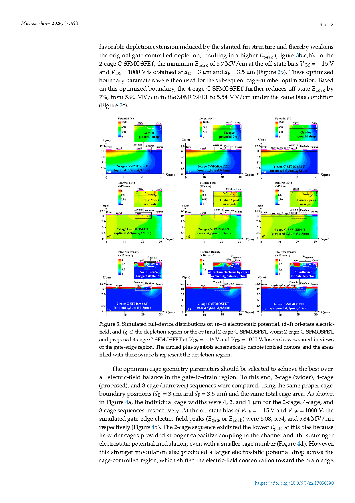
Figure 3. Simulated full-device distributions of: (a–c) electrostatic potential, (d–f) off-state electric-field, and (g–i) the depletion region of the optimal 2-cage C-SFMOSFET, worst 2-cage C-SFMOSFET, and proposed 4-cage C-SFMOSFET at VGS = −15 V and VDS = 1000 V. Insets show zoomed-in views of the gate-edge region. The circled plus symbols schematically denote ionized donors, and the areas filled with these symbols represent the depletion region.
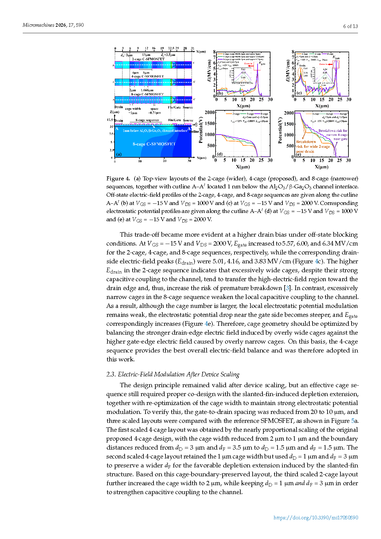
Figure 4. (a) Top-view layouts of the 2-cage (wider), 4-cage (proposed), and 8-cage (narrower) sequences, together with cutline A–A′ located 1 nm below the Al₂O₃/β‑Ga₂O₃ channel interface. Off-state electric-field profiles of the 2-cage, 4-cage, and 8-cage sequences are given along the cutline A–A′ (b) at VGS = −15 V and VDS = 1000 V and (c) at VGS = −15 V and VDS = 2000 V. Corresponding electrostatic potential profiles are given along the cutline A–A′ (d) at VGS = −15 V and VDS = 1000 V and (e) at VGS = −15 V and VDS = 2000 V.
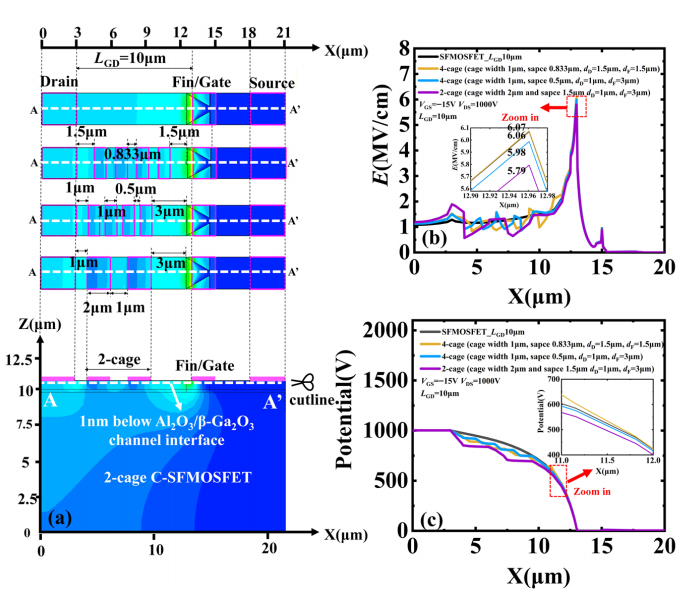
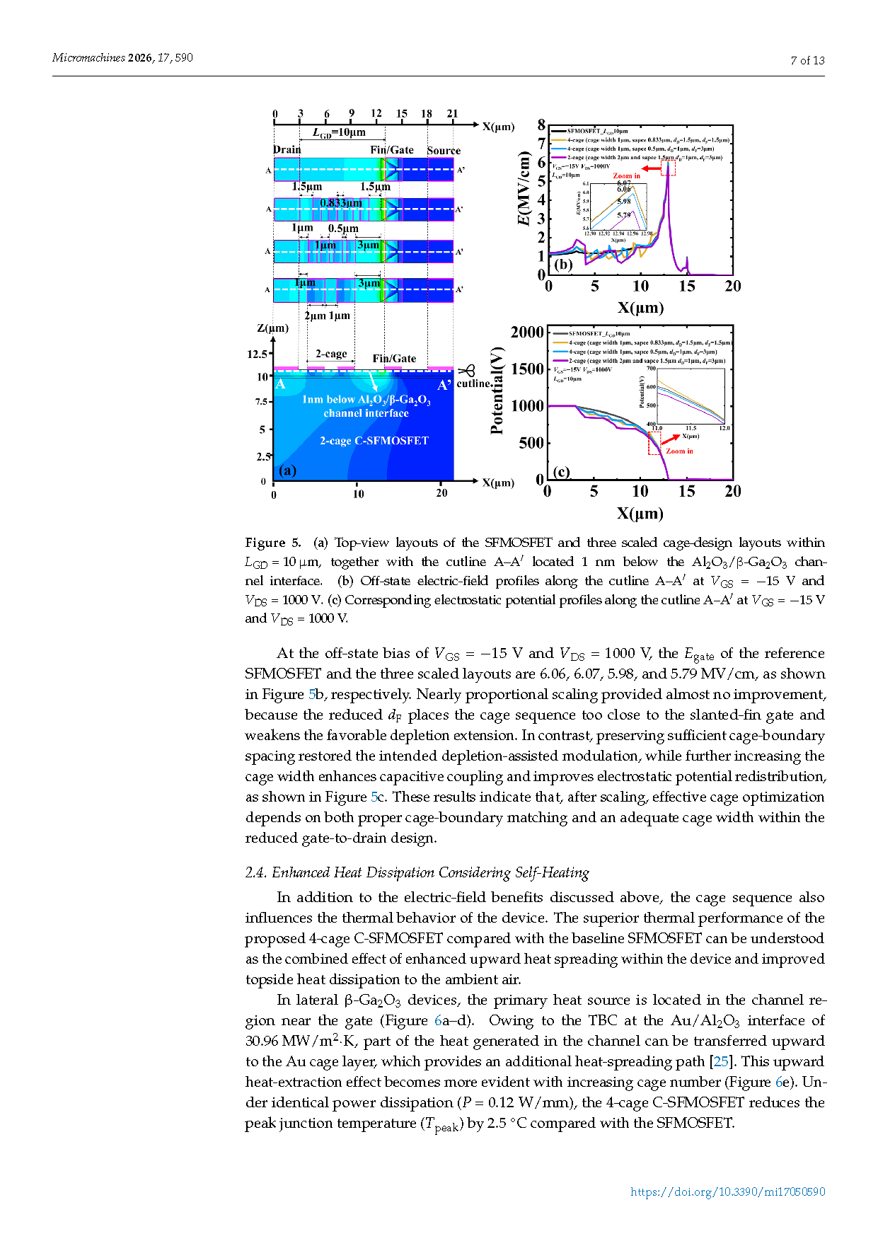
Figure 5. (a) Top-view layouts of the SFMOSFET and three scaled cage-design layouts within LGD = 10 μm, together with the cutline A–A′ located 1 nm below the Al₂O₃/β‑Ga₂O₃ channel interface. (b) Off-state electric-field profiles along the cutline A–A′ at VGS = −15 V and VDS = 1000 V. (c) Corresponding electrostatic potential profiles along the cutline A–A′ at VGS = −15 V and VDS = 1000 V.
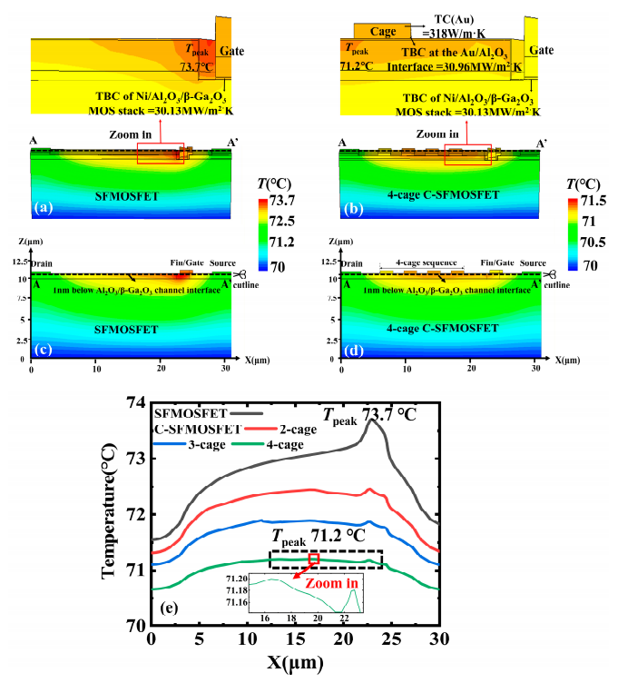
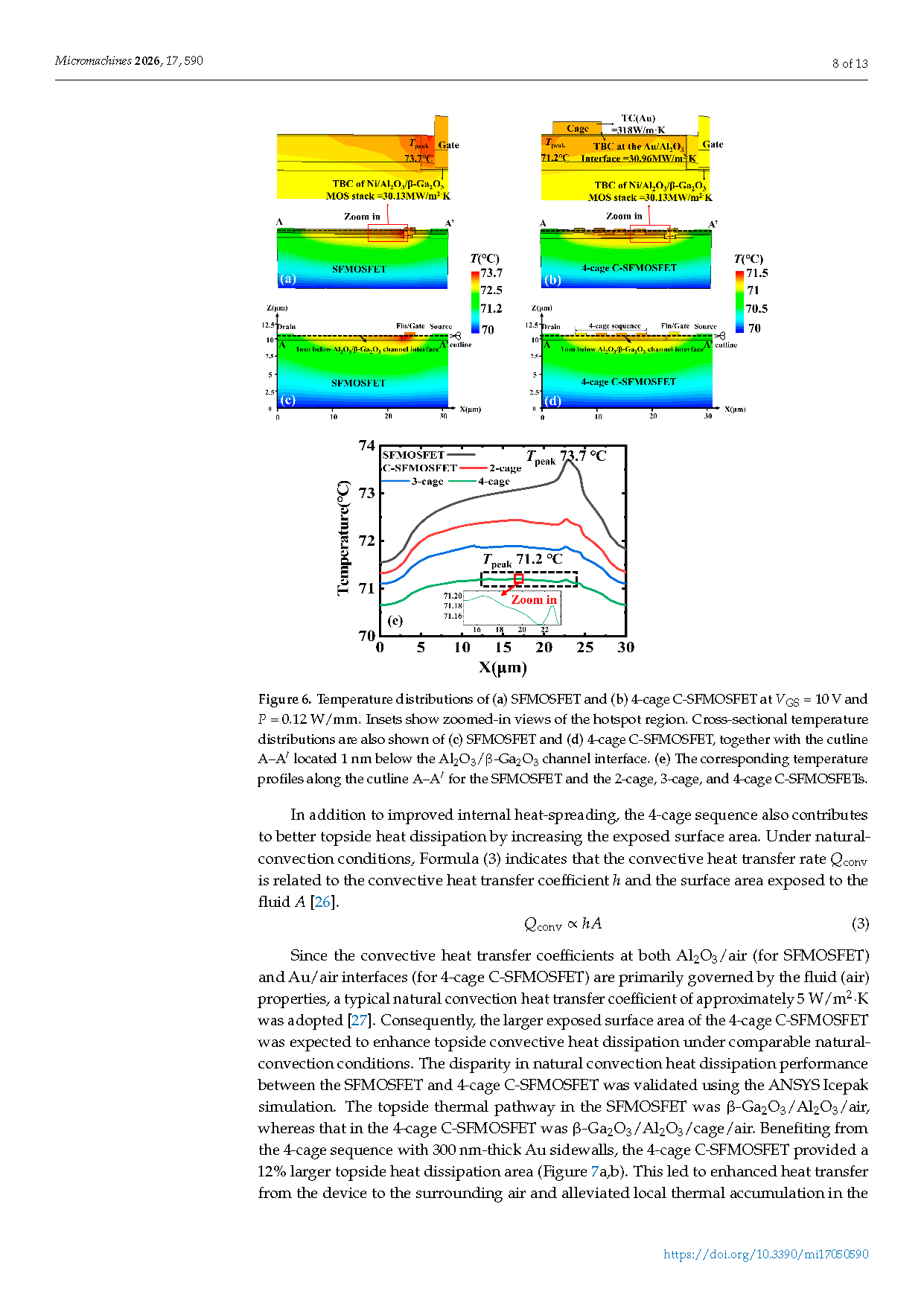
Figure 6. Temperature distributions of (a) SFMOSFET and (b) 4-cage C-SFMOSFET at VGS = 10 V and P = 0.12 W/mm. Insets show zoomed-in views of the hotspot region. Cross-sectional temperature distributions are also shown of (c) SFMOSFET and (d) 4-cage C-SFMOSFET, together with the cutline A–A′ located 1 nm below the Al₂O₃/β‑Ga₂O₃ channel interface. (e) The corresponding temperature profiles along the cutline A–A′ for the SFMOSFET and the 2-cage, 3-cage, and 4-cage C-SFMOSFETs.
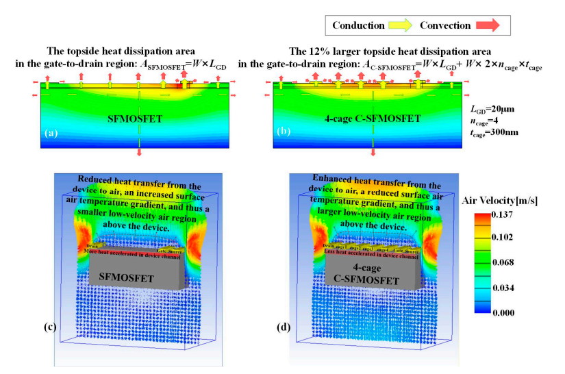
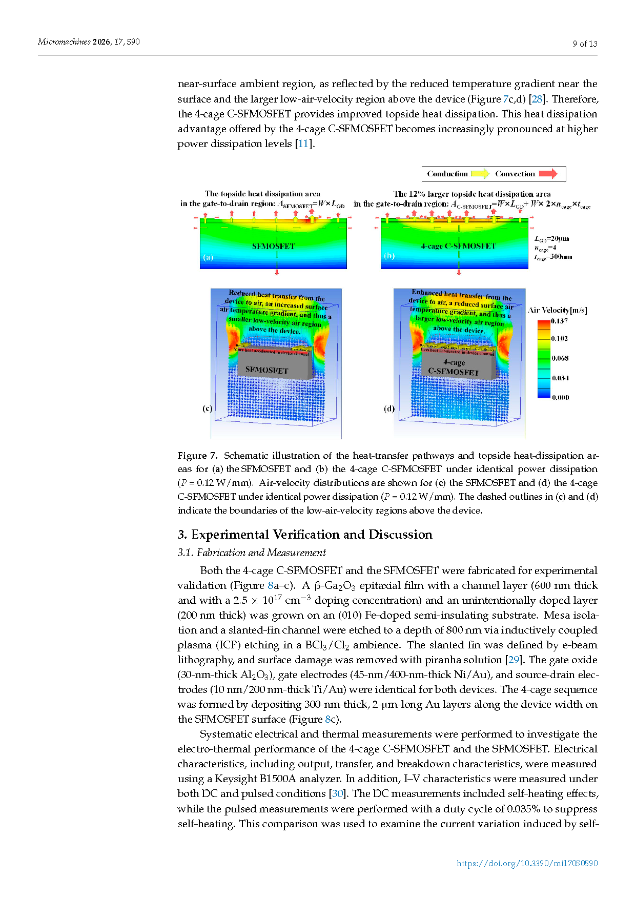
Figure 7. Schematic illustration of the heat-transfer pathways and topside heat-dissipation areas for (a) the SFMOSFET and (b) the 4-cage C-SFMOSFET under identical power dissipation (P = 0.12 W/mm). Air-velocity distributions are shown for (c) the SFMOSFET and (d) the 4-cage C-SFMOSFET under identical power dissipation (P = 0.12 W/mm). The dashed outlines in (c) and (d) indicate the boundaries of the low-air-velocity regions above the device.
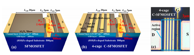
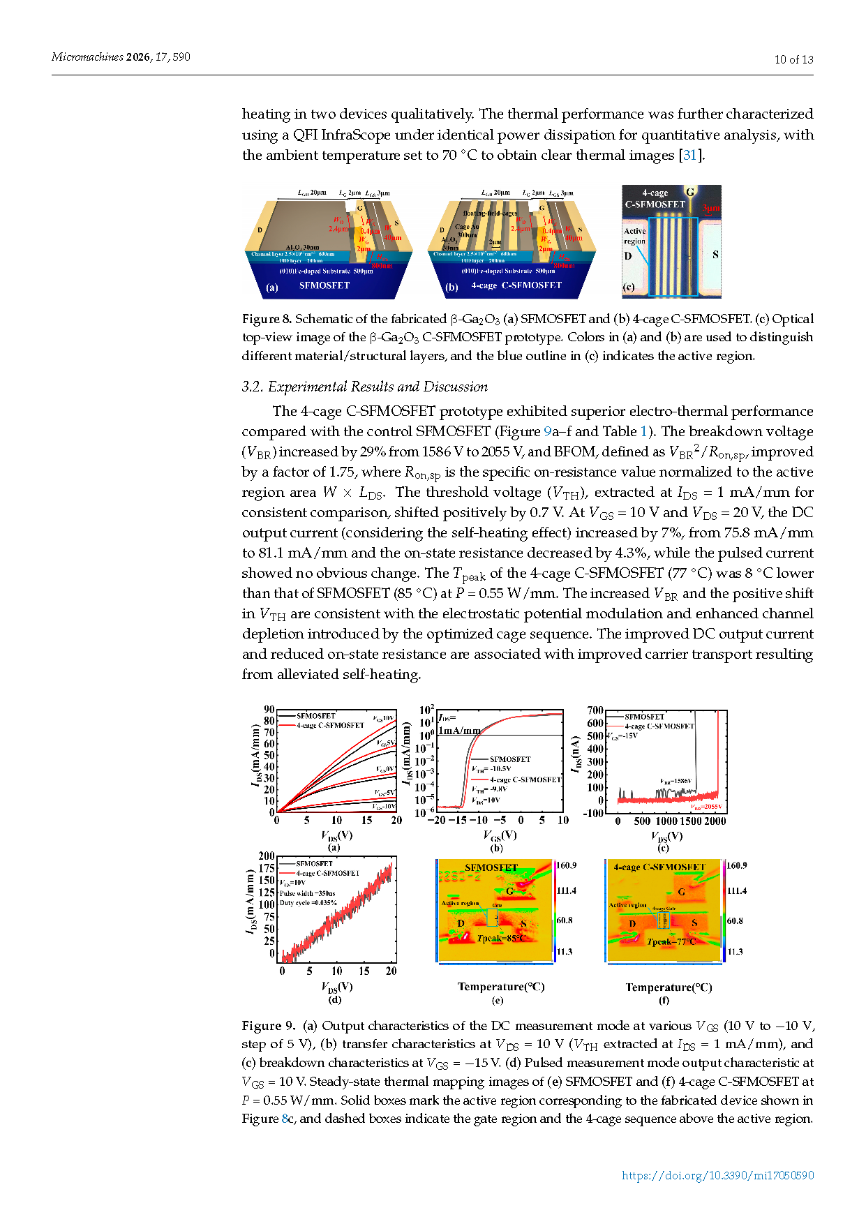
Figure 8. Schematic of the fabricated β‑Ga₂O₃ (a) SFMOSFET and (b) 4-cage C-SFMOSFET. (c) Optical top-view image of the β‑Ga₂O₃ C-SFMOSFET prototype. Colors in (a) and (b) are used to distinguish different material/structural layers, and the blue outline in (c) indicates the active region.
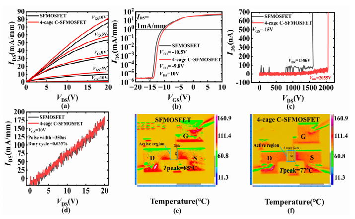
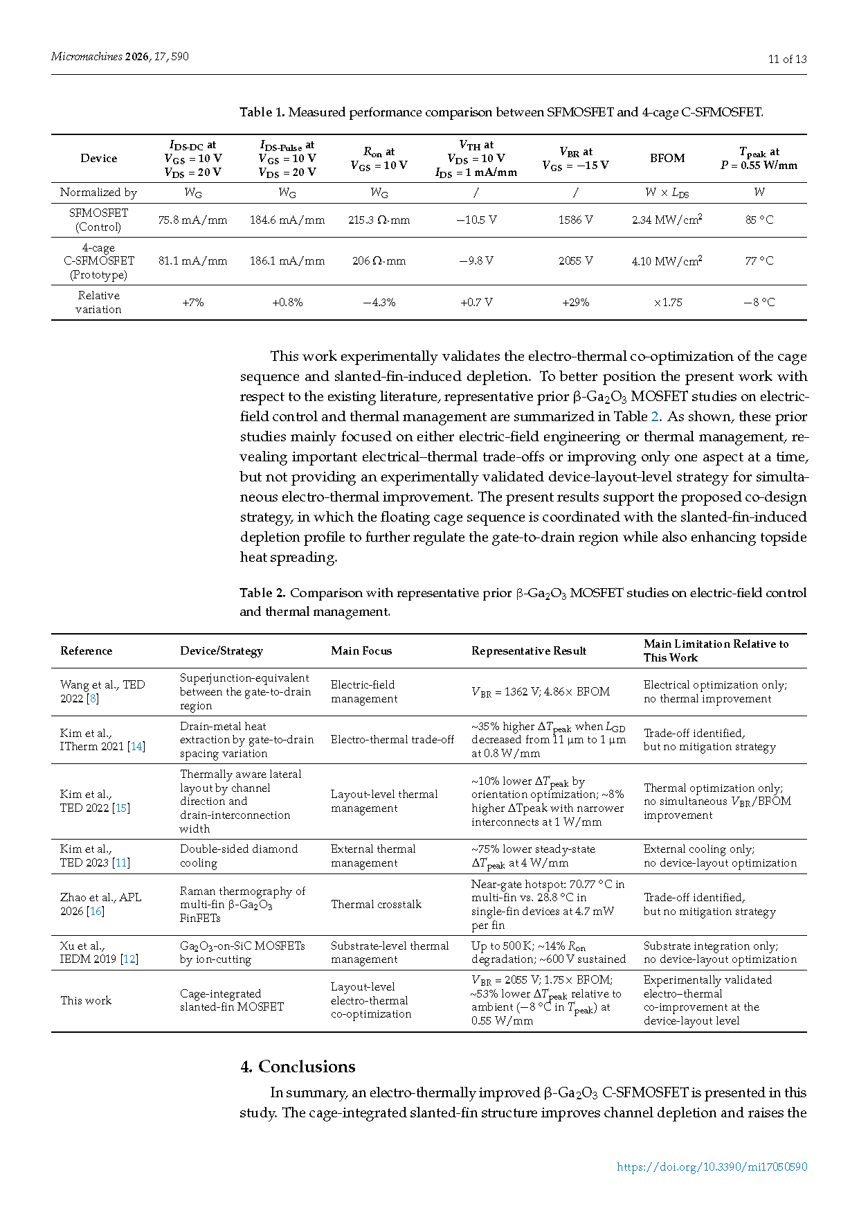
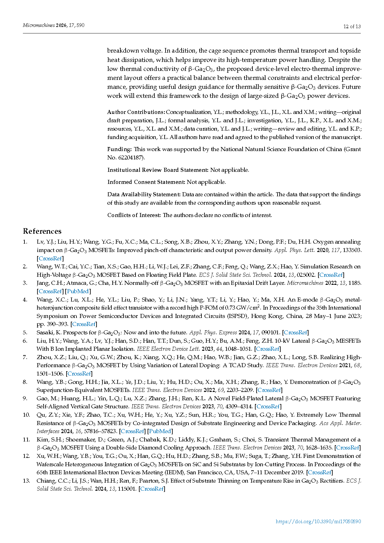
Figure 9. (a) Output characteristics of the DC measurement mode at various VGS (10 V to −10 V, step of 5 V), (b) transfer characteristics at VDS = 10 V (VTH extracted at IDS = 1 mA/mm), and (c) breakdown characteristics at VGS = −15 V. (d) Pulsed measurement mode output characteristic at VGS = 10 V. Steady-state thermal mapping images of (e) SFMOSFET and (f) 4-cage C-SFMOSFET at P = 0.55 W/mm. Solid boxes mark the active region corresponding to the fabricated device shown in Figure 8c, and dashed boxes indicate the gate region and the 4-cage sequence above the active region.
DOI:
doi.org/10.3390/mi17050590