Paper Sharing
【Domestic Papers】Controllable phase transition in Sn-doped Ga₂O₃ film induced by mixed nitrogen-oxygen growth atmosphere
日期:2026-06-16阅读:41
Researchers from Zhejiang Normal University and Shanghai University have published a dissertation titled Controllable phase transition in Sn-doped Ga₂O₃ film induced by mixed nitrogen-oxygen growth atmosphere in Vacuum.
Background
Ultra-wide bandgap semiconductors drive the development of next-generation high-power electronic and deep-ultraviolet optoelectronic devices. As one of the most promising candidates for the post-Moore era, β-Ga₂O₃ possesses an ultra-wide bandgap and extremely high critical breakdown electric field, and it has the best thermodynamic stability among five crystal phases of Ga₂O₃. Nevertheless, its low intrinsic carrier concentration restricts practical applications in high-power devices.
Tin (Sn) doping is widely used to improve the n-type conductivity of Ga₂O₃, for Sn can donate extra electrons via aliovalent substitution. Unfortunately, high Sn doping content will form metastable ε-Ga₂O₃ and lead to mixed phases, which degrades device performance.
Existing studies mainly focus on the effects of cation doping and growth temperature on Ga₂O₃ crystal phases, while the regulation effect of growth atmosphere is rarely investigated. In this work, the team systematically studied Sn-doped Ga₂O₃ films under different N₂/O₂ ratios to develop a simple and controllable strategy for crystal phase modulation.
Abstract
Although β-Ga₂O₃ holds distinct advantages for high-power electronics and deep-ultraviolet photodetection, its low intrinsic carrier concentration limits practical applications. Tin (Sn) doping is commonly employed to enhance n-type conductivity; however, this approach tends to induce the formation of metastable ε-Ga₂O₃ thereby degrading device performance. To date, a simple and controllable strategy to suppress this undesirable phase transition remains lacking. Herein, we demonstrate that the phase evolution of Sn-doped Ga₂O₃ thin films can be effectively regulated by tuning the N₂/O₂ growth atmosphere during deposition. Specifically, as the N₂ partial pressure increases from 0 to 0.009 mbar, the transformation from the ε-phase to the β-phase is markedly promoted, with the β-phase fraction reaching 100%. SIMS measurements reveal a nitrogen doping concentration as high as 6 × 10²⁰ atoms/cm³. This phase-transition control method offers valuable guidance for the fabrication of high-performance Ga₂O₃-based devices.
Highlights
A novel strategy using N₂/O₂ mixed atmosphere to modulate crystal phases of Sn-doped Ga₂O₃ is proposed, without changing growth temperature and Sn doping concentration.
Increasing N₂ partial pressure can realize complete phase transition from ε-Ga₂O₃ to β-Ga₂O₃; excessive nitrogen will turn the film into amorphous state.
Control experiments exclude the interference of air pressure and argon, proving nitrogen doping is the key factor for phase transition. The phase transition mechanism that N atoms replace O sites and destroy octahedral Ga coordination is clarified.
Nitrogen doping increases oxygen vacancy concentration, narrows optical bandgap, and improves dark current, photocurrent and photoresponse properties of the films.
Conclusion
In this study, we demonstrate the existence of a controllable phase transition in tin-doped gallium oxide (Ga₂O₃) thin films prepared by pulsed laser deposition technology in a mixed N₂/O₂ atmosphere, driven by thermodynamics. By simply adjusting the nitrogen-to-oxygen ratio, the crystal phase of the thin films can be tuned from the ε phase system to a mixed phase, and ultimately to a pure β phase. Comprehensive TEM-EDS and SIMS analysis confirm that the thin films contain high concentrations of nitrogen doping. With the incorporation of nitrogen, it occupies the O sites in Ga₂O₃, especially the octahedral sites of Ga, driving the sample to transition to the thermodynamically more stable β phase. This study not only provides a simple and effective strategy for phase engineering of gallium oxide thin films but also offers new insights into the role of non-reactive gases in oxide thin film growth, paving the way for the synthesis and design of high-performance gallium oxide-based devices through atmosphere control.
Project Support
This work is supported by the Zhejiang Province Natural Science Foundation Joint Fund Project (Grants No: JHSZ26F040001), Jinhua City Science and Technology Plan Project (Grants No: 2025-4-186, 2025-4-185), Scientific Research Fund of Zhejiang Provincial Education Department (Grants No: Y202455408), National Natural Science Foundation of China (Grants No: 12304181, 12574178, 11604201), and FERMION INSTRUMENTS (SHANGHAI) CO., LTD.
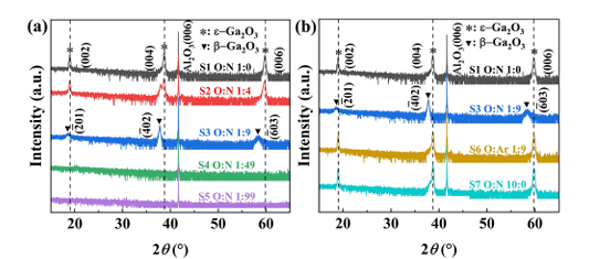
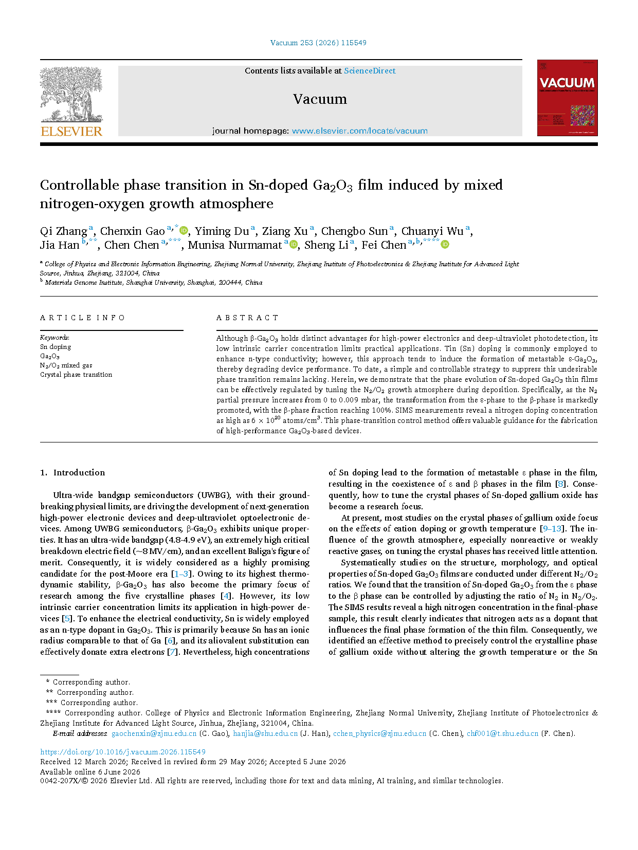
Figure 1 (a) XRD patterns of S1~S5, showing the phase evolution of Ga₂O₃ films among the ε, β and amorphous phases; (b) XRD patterns of S1, S3, S6 and S7 with the addition of control group S6 and control group S7.
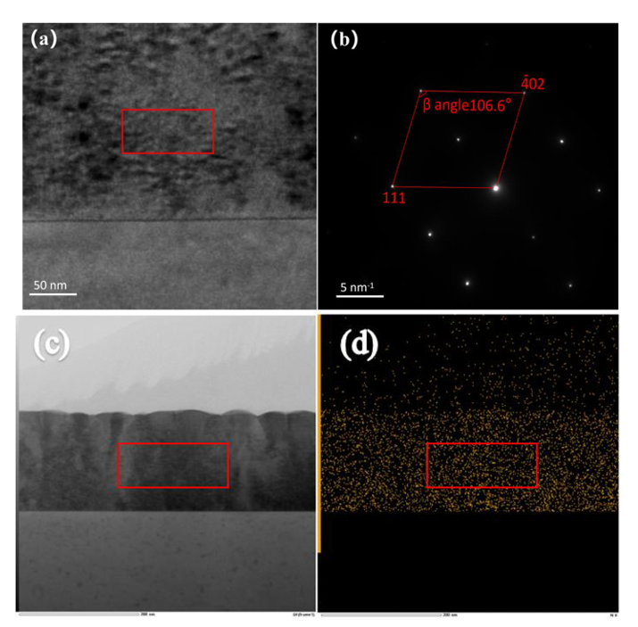
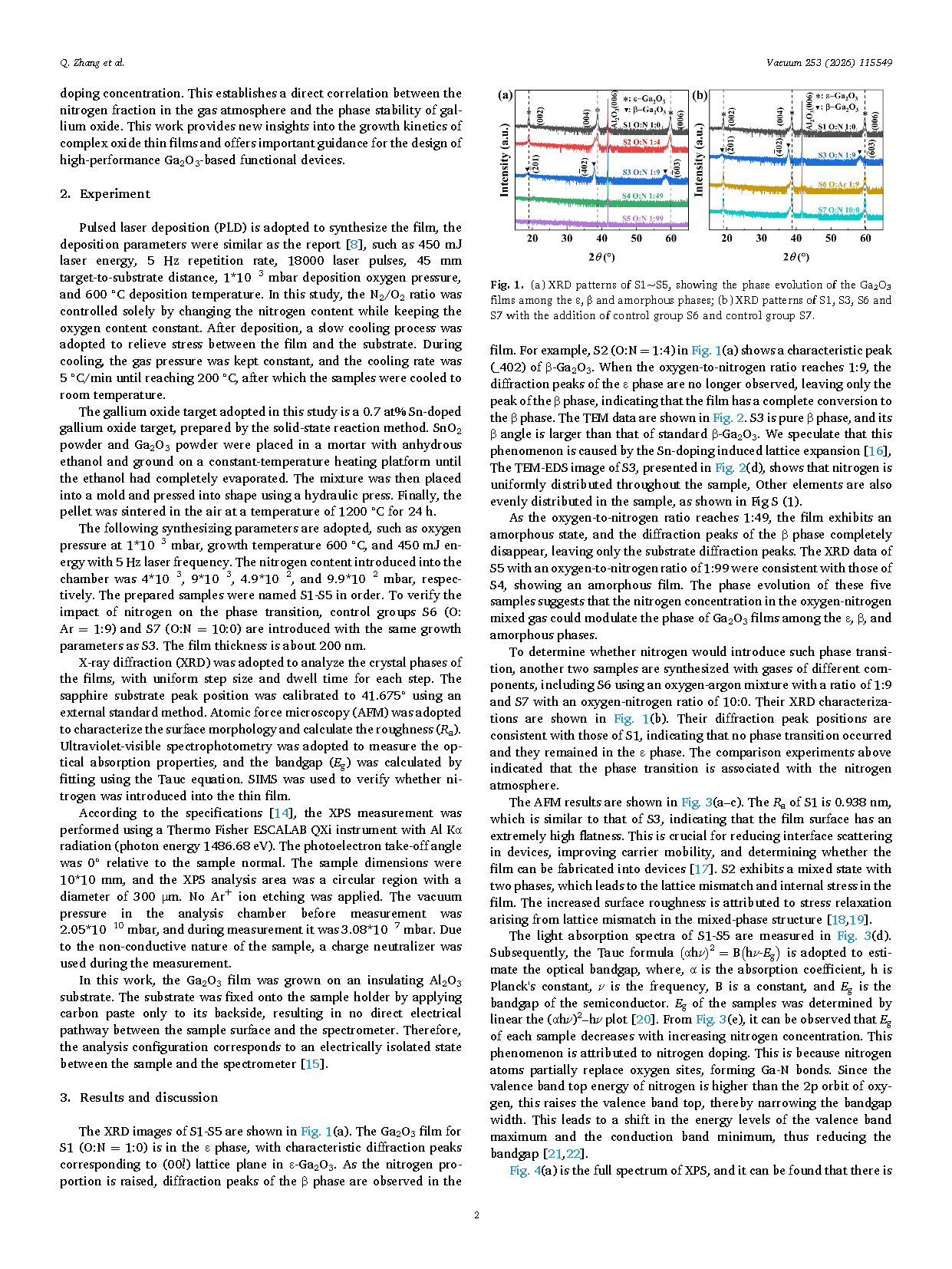
Figure 2 (a) TEM image of the film cross-section, with the red box indicating the approximate range selected for diffraction; (b) Selected diffraction pattern corresponding to the film cross-section, with the lattice plane indices corresponding to their spacings being (4̄02) and (111), and the beta angle of the monoclinic β phase is 106.6°; (c) TEM-EDS sample morphology image; (d) Distribution map of N element.
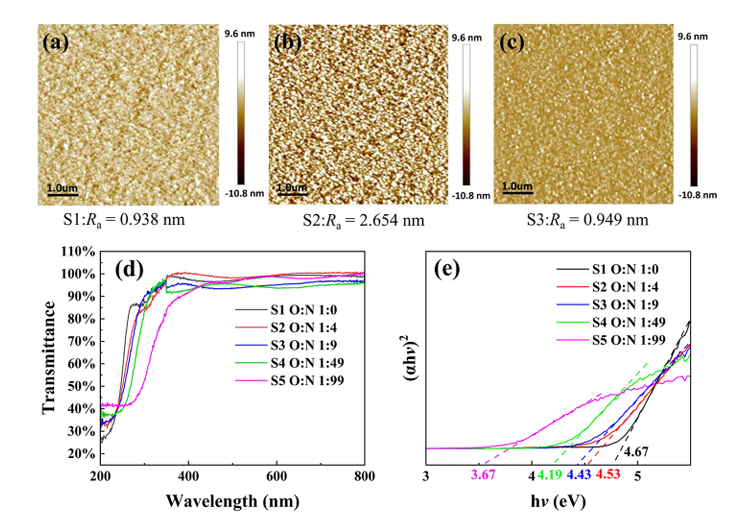
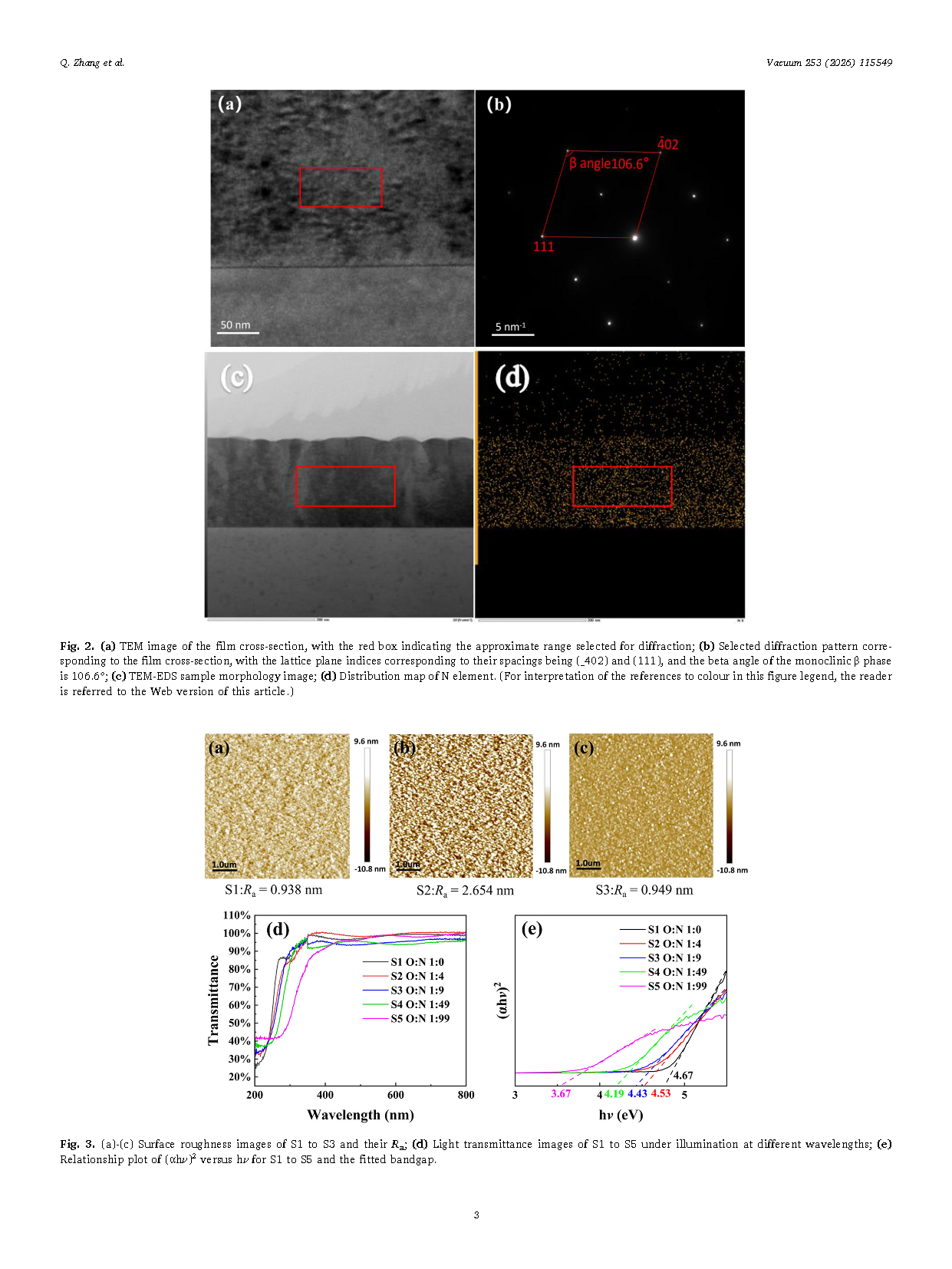
Figure 3 (a)-(c) Surface roughness images of S1 to S3 and their Rₐ; (d) Light transmittance images of S1 to S5 under illumination at different wavelengths; (e) Relationship plot of (αhν)² versus hν for S1 to S5 and the fitted bandgap.
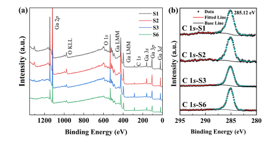
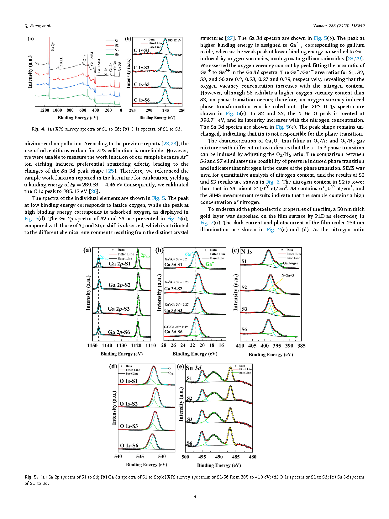
Figure 4 (a) XPS survey spectra of S1 to S6; (b) C 1s spectra of S1 to S6.
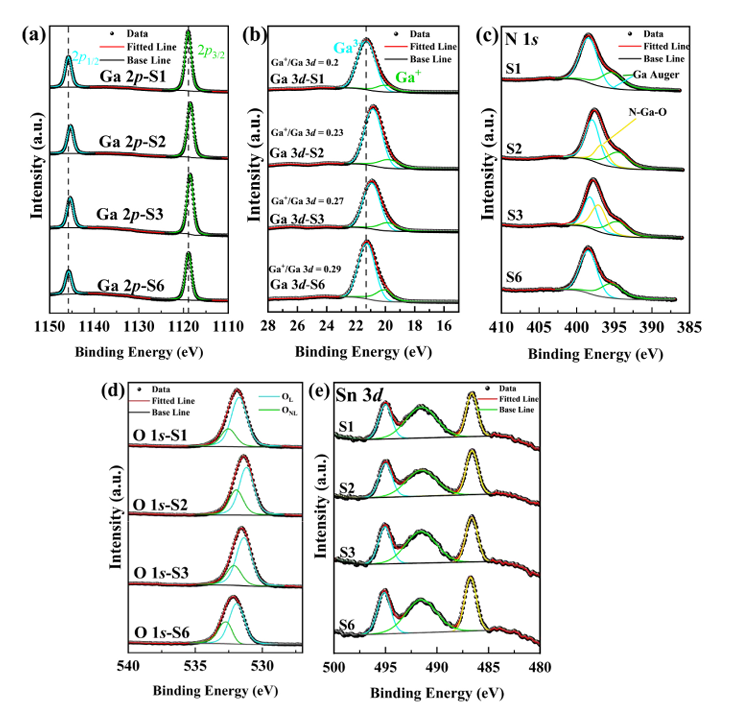
Figure 5 (a) Ga 2p spectra of S1 to S6; (b) Ga 3d spectra of S1 to S6; (c) XPS survey spectrum of S1-S6 from 385 to 410 eV; (d) O 1s spectra of S1 to S6; (e) Sn 3d spectra of S1 to S6.
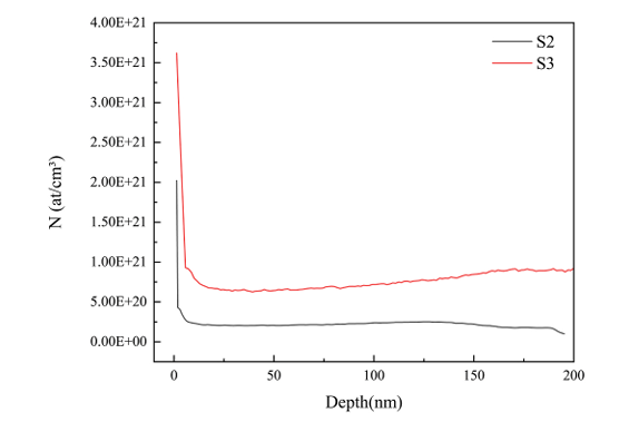
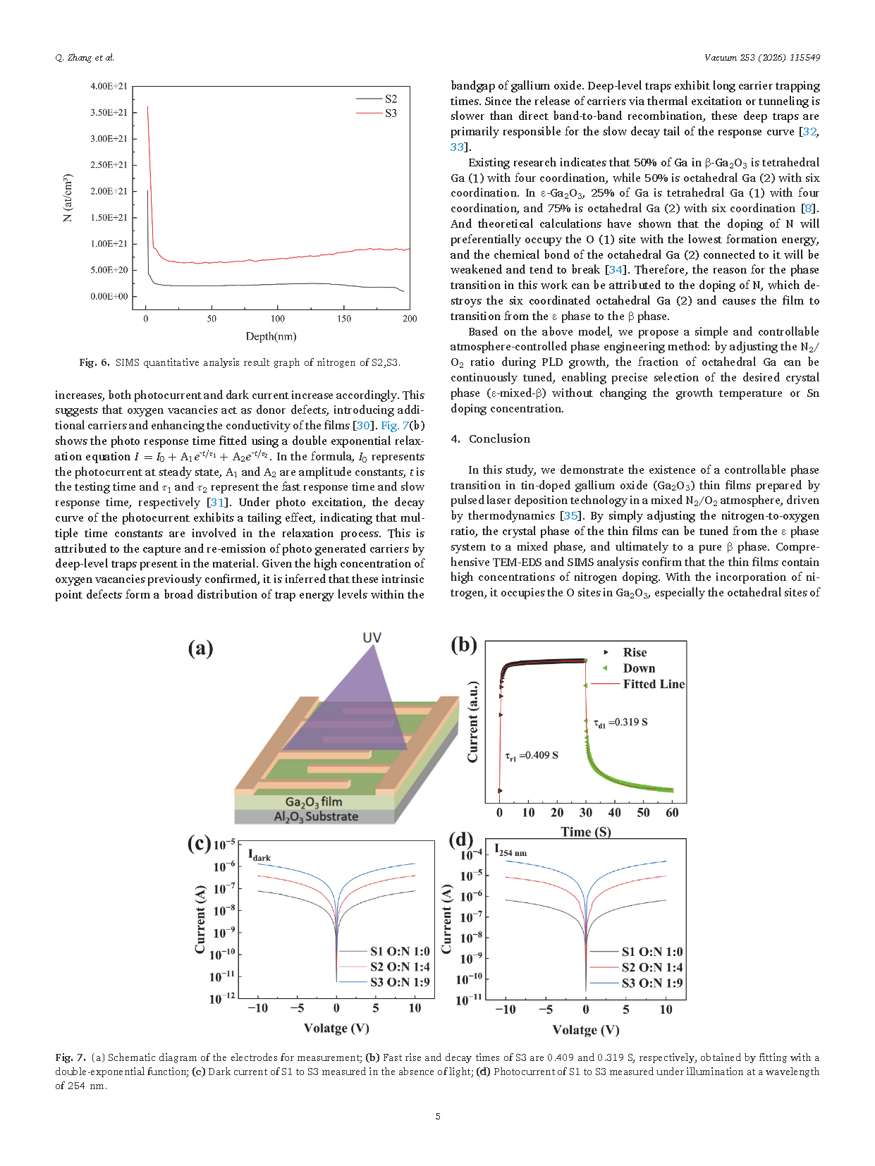
Figure 6 SIMS quantitative analysis result graph of nitrogen of S2,S3.
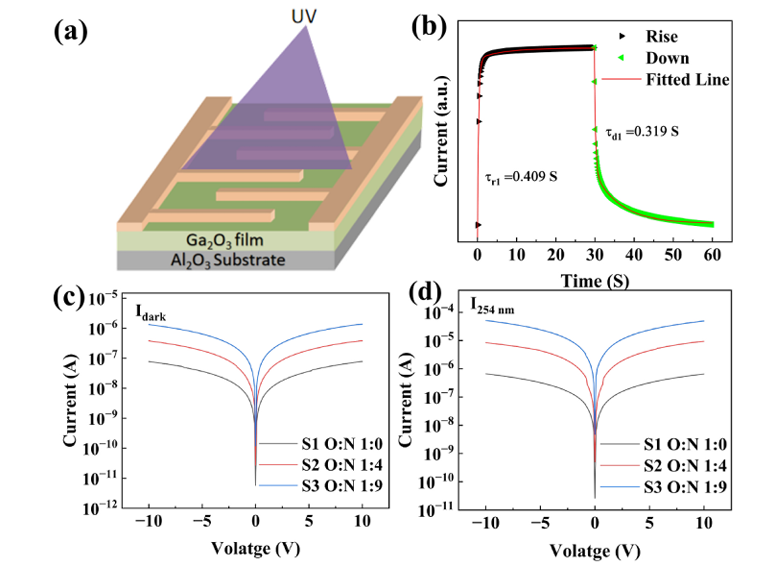
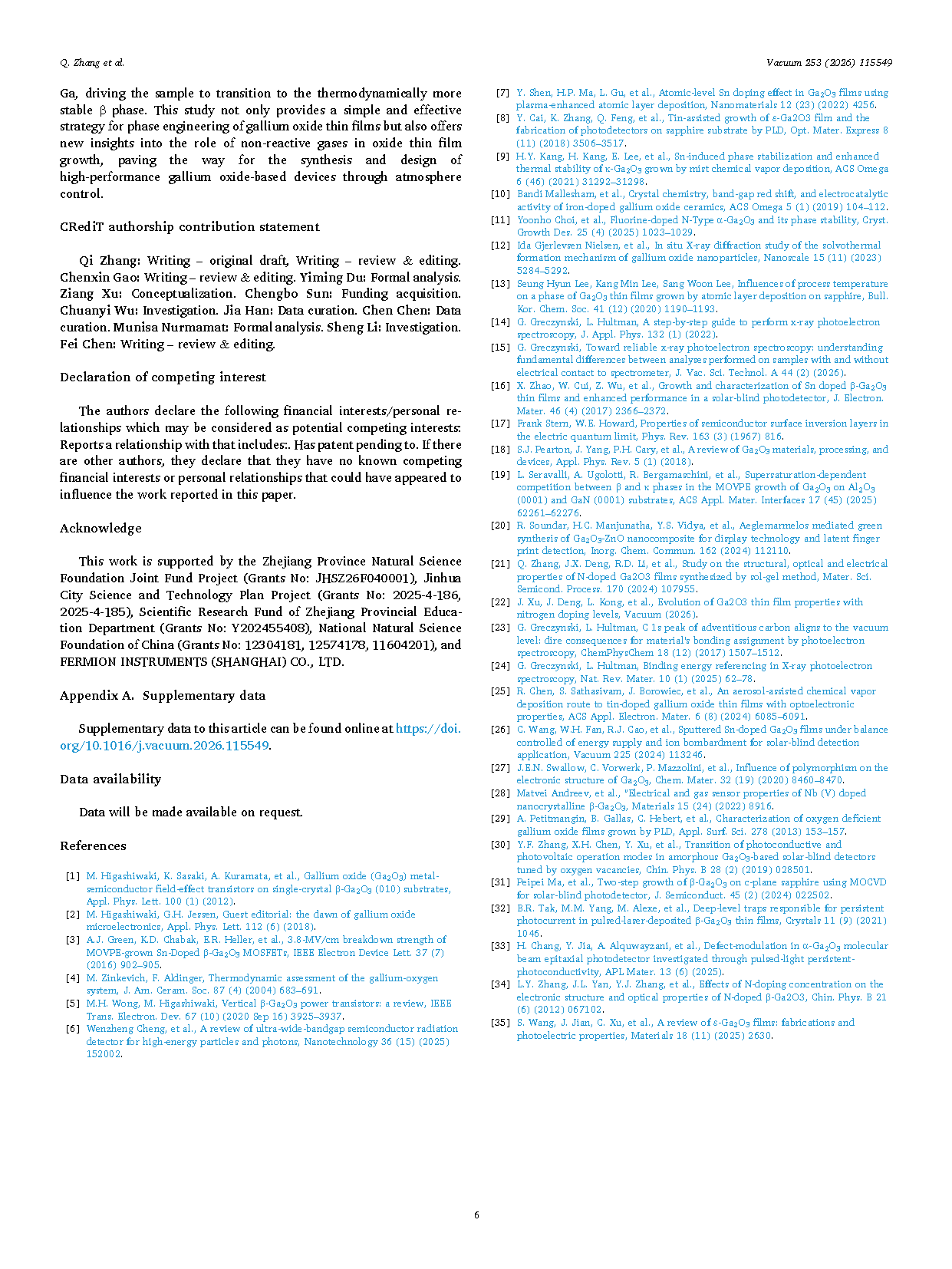
Figure 7 (a) Schematic diagram of the electrodes for measurement; (b) Fast rise and decay times of S3 are 0.409 and 0.319 S, respectively, obtained by fitting with a double-exponential function; (c) Dark current of S1 to S3 measured in the absence of light; (d) Photocurrent of S1 to S3 measured under illumination at a wavelength of 254 nm.
DOI:
doi.org/10.1016/j.vacuum.2026.115549