Paper Sharing
【International Papers】Microwave plasma CVD growth and characterization of polycrystalline diamond films on β-Ga₂O₃
日期:2026-06-18阅读:38
Researchers from University of Massachusetts Lowell have published a dissertation titled "Microwave plasma CVD growth and characterization of polycrystalline diamond films on β-Ga₂O₃" in Applied Physics Letters.
Background
β-Ga₂O₃ is an ultra-wide bandgap semiconductor. It has a bandgap of 4.8 eV, high critical electric field and low-cost melt-grown large-area substrates, which makes it promising for next-generation power electronic devices. However, its low intrinsic thermal conductivity causes local overheating under high power, leading to device degradation and poor reliability. Diamond features ultrahigh thermal conductivity, wide bandgap, great mechanical strength and chemical stability, which is an excellent material for thermal management. Microwave plasma CVD has been successfully used for diamond integration on GaN, while it is challenging to grow diamond on β-Ga₂O₃ due to surface energy mismatch. Previous studies mainly focus on the early nucleation stage. There is a lack of systematic research on the influence of deposition conditions and dielectric interlayers on the morphology, grain structure, phase composition and optical properties of diamond films, which hinders the development of thermal management solutions for β-Ga₂O₃ power devices.
Abstract
The integration of diamond with β-Ga₂O₃ presents a promising pathway to enhance thermal management in high-power electronic devices, where the inherently low thermal conductivity of β-Ga₂O₃ can lead to localized self-heating and elevated junction temperatures. In this work, we demonstrate a scalable, low-damage approach to integrate polycrystalline diamond films on (010) β-Ga₂O₃ substrates via microwave plasma chemical vapor deposition, employing dielectric interlayers and polymer-assisted electrostatic nanodiamond seeding to systematically evaluate the impact of growth conditions on film morphology, grain evolution, phase purity, and optical characteristics. At the growth temperature of 800 °C, progressive grain coarsening is observed with extended deposition, with lateral grain size increasing from 37.6 nm (53 nm thickness) to 192.5 nm for an 886 nm film. This microstructural evolution is accompanied by narrowing of the diamond peak and a monotonic increase in sp³-phase fraction from 95.9% to as high as 98.9%, indicating continued suppression of non-diamond carbon with prolonged growth. Comparison of SiO₂ and SiNₓ interlayers under identical growth conditions shows only marginal differences in grain size and phase purity, indicating limited interlayer influence once high nucleation density is established. Importantly, diamond films exhibiting >96% sp³-phase content were achieved at substrate temperatures as low as 480 °C, highlighting the viability of diamond-on-Ga₂O₃ integration under reduced thermal budgets. These findings establish a robust, scalable platform for integrating diamond on β-Ga₂O₃, supporting the development of next-generation power and RF devices with improved thermal management.
Highlights
Propose a low-damage and scalable MPCVD method to grow polycrystalline diamond films on (010) β-Ga₂O₃ substrates with dielectric interlayers and polymer-assisted nanodiamond seeding.
Reveal the evolution rule of grain size, surface morphology and sp³ phase purity of diamond films with deposition time at 800 °C.
Verify that SiO₂ and SiNₓ interlayers have negligible effect on diamond film quality after forming high nucleation density.
Realize high-purity diamond films with over 96% sp³ fraction at the low temperature of 480 °C.
Conclusion
In summary, this work presents a comprehensive investigation into the MPCVD growth of diamond films on β-Ga₂O₃, demonstrating how processing conditions and interface engineering influence grain development, surface characteristics, and optical response. Thickness-dependent studies reveal a steady progression from densely nucleated nanocrystalline films to well-faceted surfaces, accompanied by lateral grain expansion and improved ordering during extended growth at a fixed temperature. As substrate temperature increases, enhanced surface mobility promotes grain coarsening and phase refinement, accompanied by higher growth rates and the resulting increase in film thickness. Notably, continuous and phase-pure diamond films are achievable even at low temperature (480 °C), highlighting the compatibility of this approach with device processing schemes constrained by limited thermal budgets.
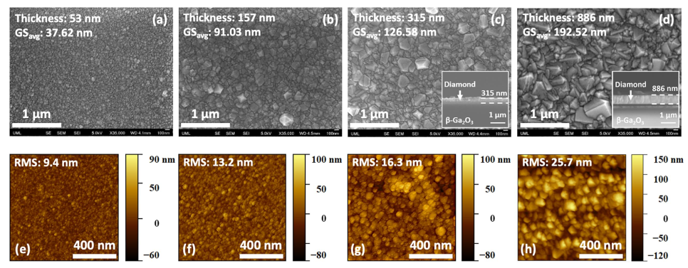
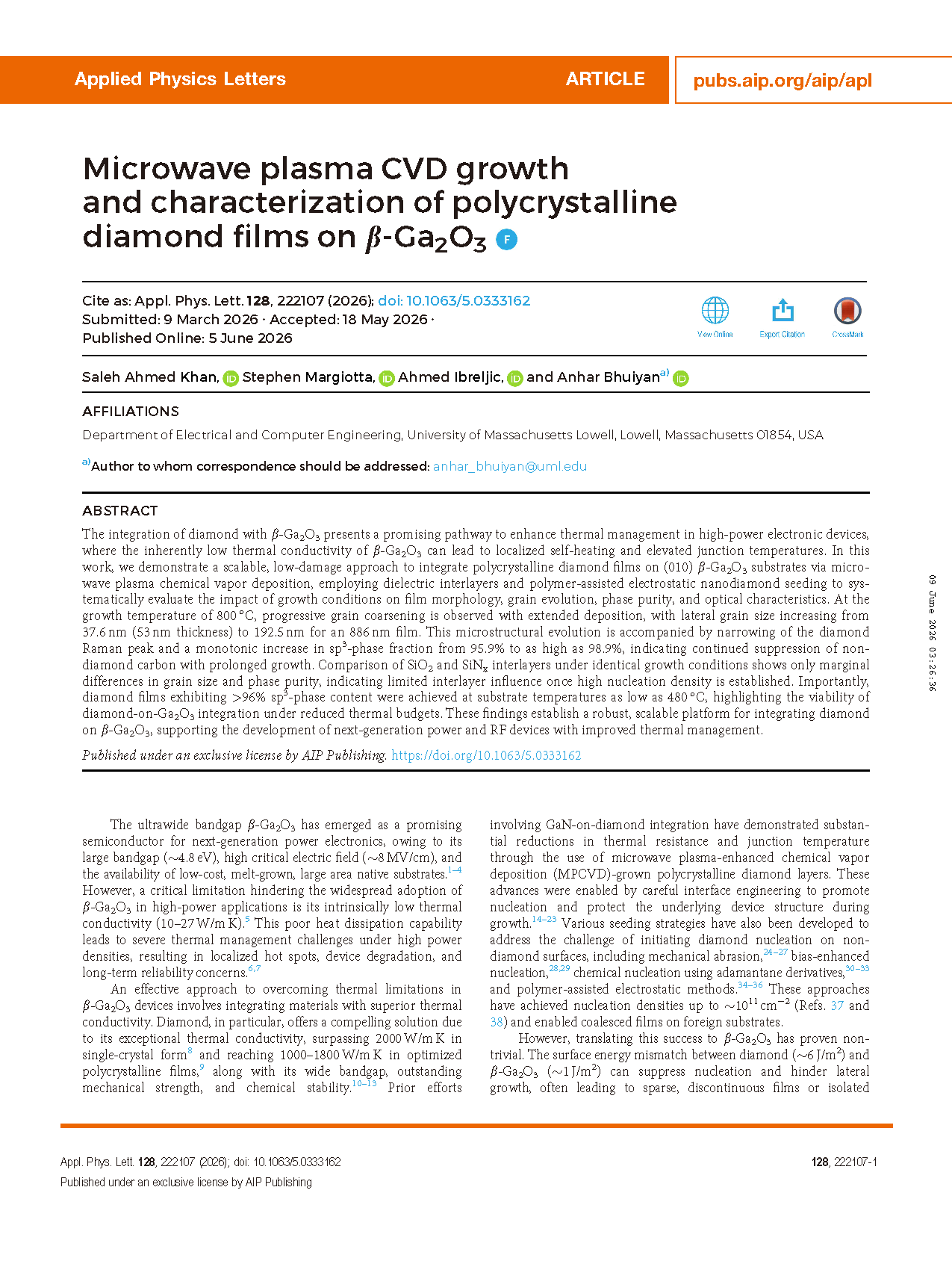
FIG. 1. Surface morphology and roughness evolution of diamond films grown at 800 C for 10, 30, 60, and 150 min: (a)–(d) SEM images and (e)–(h) corresponding AFM scans showing increasing grain size, faceting, and RMS roughness.
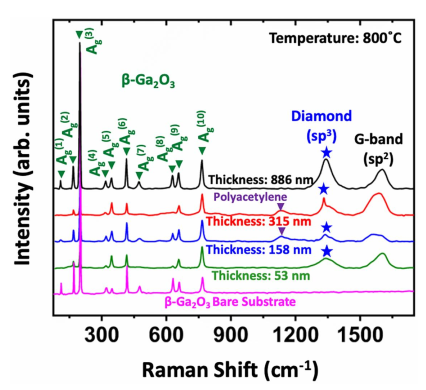
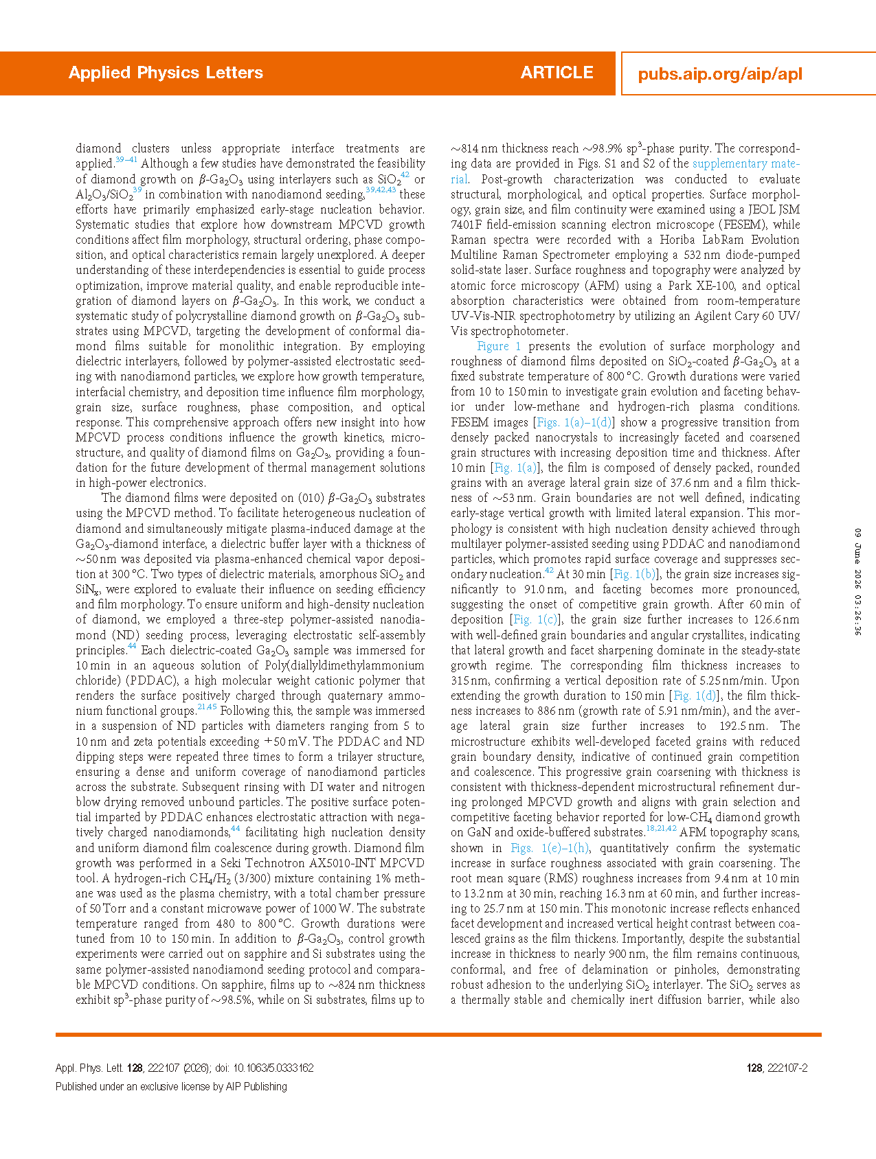
FIG. 2. Raman spectra of diamond films grown at 800 C, showing intensification of the sp³ diamond peak with increasing film thickness.
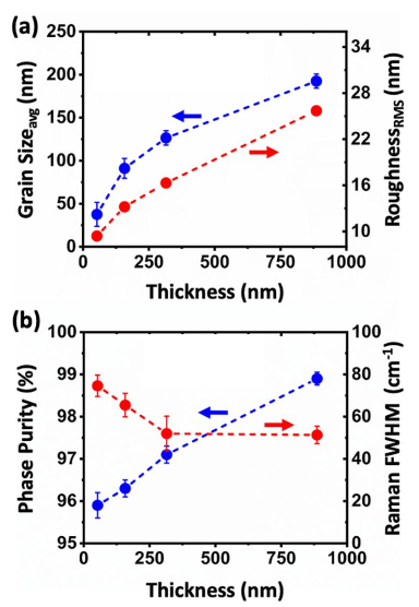
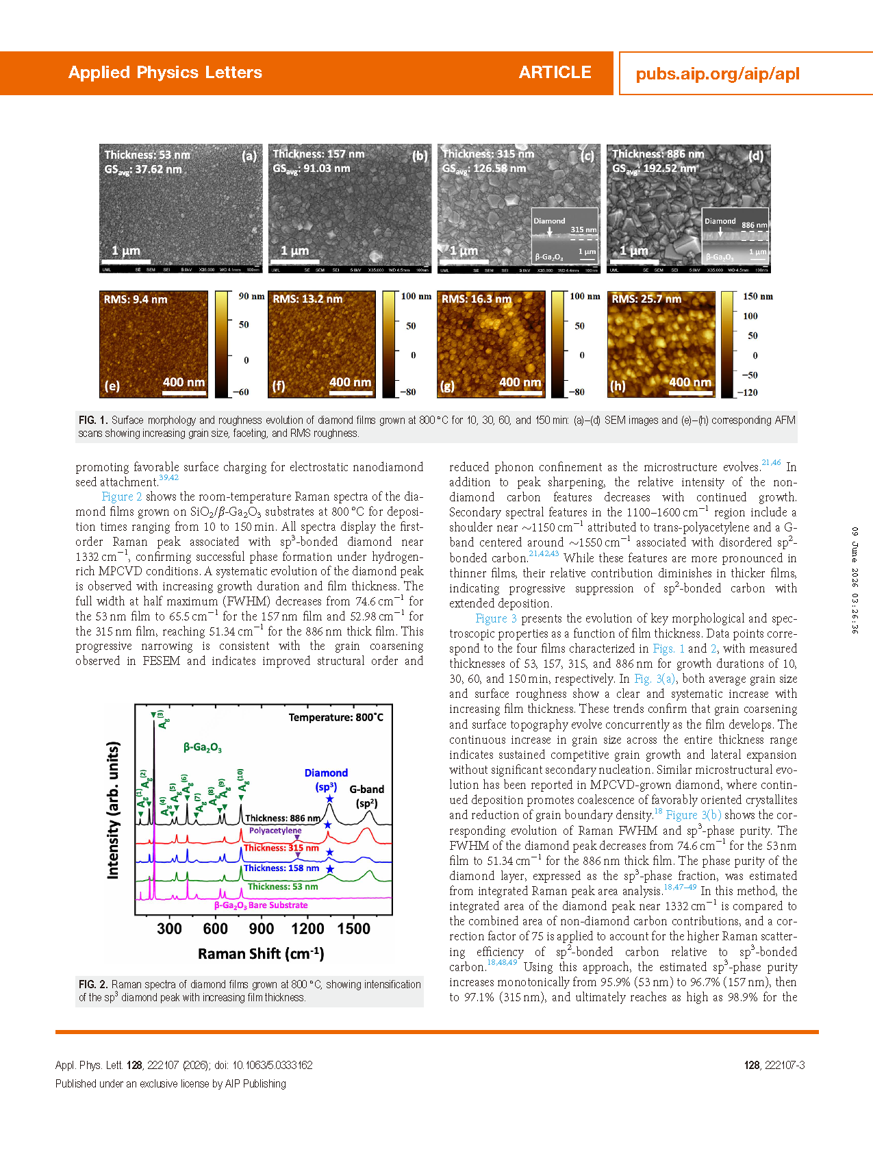
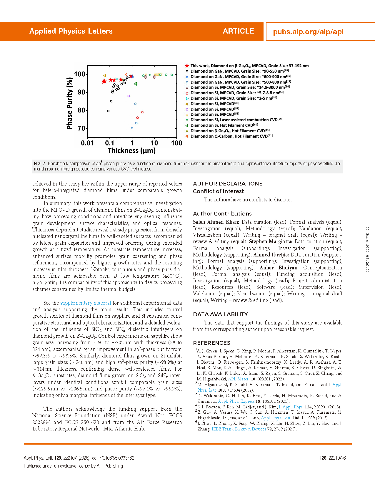
FIG. 3. Grain size, surface roughness, Raman FWHM, and sp³-phase purity as a function of diamond film thickness grown at 800 C.
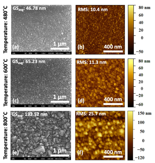
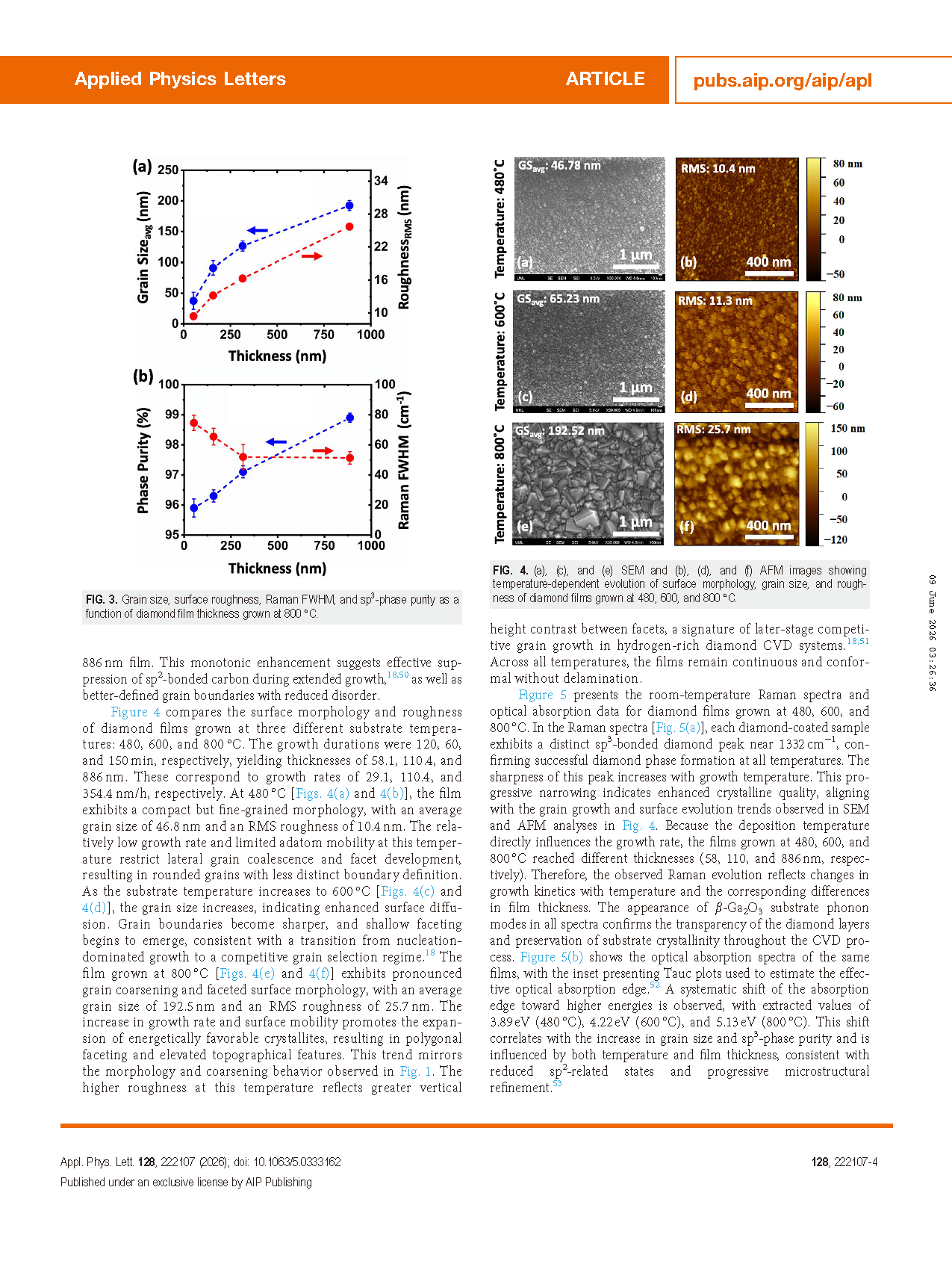
FIG. 4. (a), (c), and (e) SEM and (b), (d), and (f) AFM images showing temperature-dependent evolution of surface morphology, grain size, and roughness of diamond films grown at 480, 600, and 800 C.
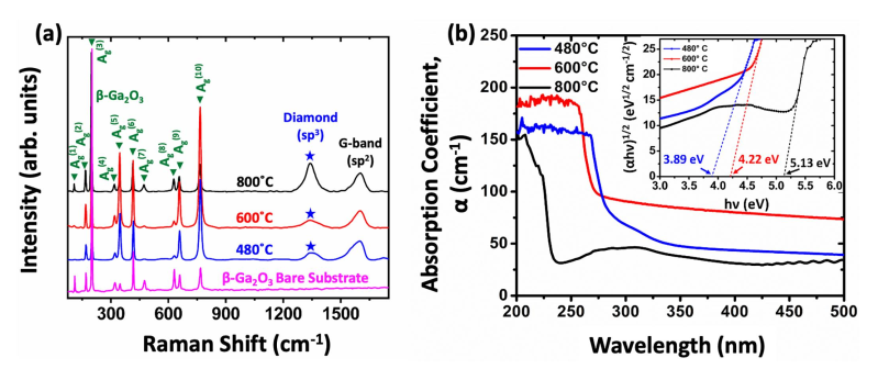
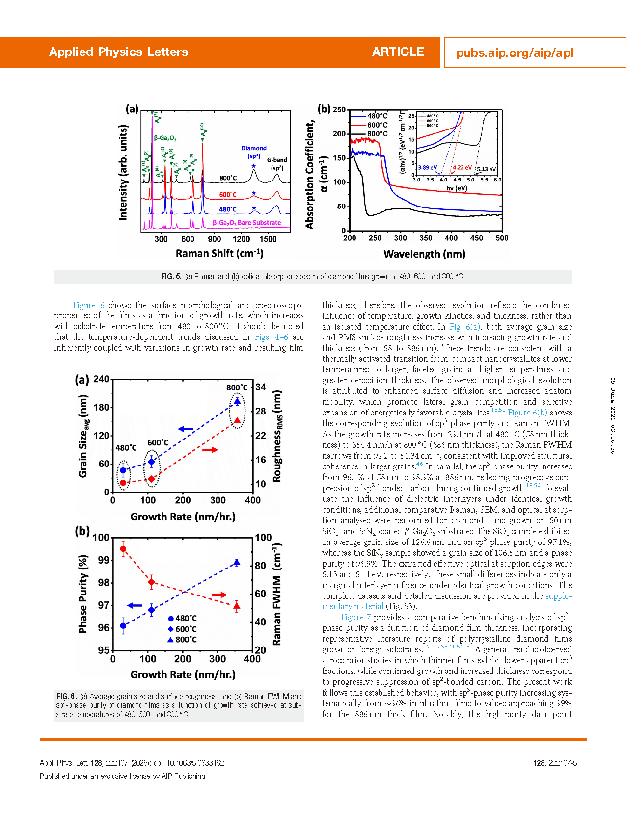
FIG. 5. (a) Raman and (b) optical absorption spectra of diamond films grown at 480, 600, and 800 C.
DOI:
doi.org/10.1063/5.0333162