


Researchers from the Jiangsu University have published a dissertation titled " Porous SiO2-Induced Field-Effect Passivation for Enhanced Ga2O3 Solar-Blind Ultraviolet Photodetectors " in Journal of Alloys and Compounds.
Background
With the rapid progress of modern science, sensing, imaging and optical communication technologies have been explored and applied. The increasing demand for spectral information acquisition promotes the development of photodetection technologies in different wavelength regions. The wavelength range of 200-280 nm is defined as the solar-blind UV band. Due to the absorption effect of the atmosphere, UV radiation with wavelength below 280 nm is extremely weak on the earth surface, endowing solar-blind UV detection technology with low background noise, high signal-to-noise ratio and strong anti-interference ability.
Ga₂O₃, an ultra-wide bandgap semiconductor with a bandgap of 4.5-5.3 eV, exhibits intrinsic absorption in the solar-blind UV region. It also has excellent thermal and chemical stability, a large breakdown electric field, high saturation electron drift velocity and relatively low cost, which makes it an ideal material for solar-blind UV photodetectors. Metal-semiconductor-metal (MSM) planar structures are widely used for Ga₂O₃ photodetectors due to simple fabrication and easy integration.
However, surface defect states generated during material preparation act as carrier trapping and recombination centers, making it difficult to simultaneously optimize responsivity and response speed. Conventional chemical passivation mainly provides physical isolation and cannot effectively suppress carrier recombination. Plasma treatment requires expensive equipment and may introduce additional defects. Field-effect passivation is a mature technology in solar cells. The porous SiO₂ film prepared by sol-gel method can introduce fixed charges to realize field-effect passivation, and its porous structure can enhance light absorption. This work adopts porous SiO₂ to modify Ga₂O₃-based MSM solar-blind UV photodetectors via surface passivation.
Abstract
In recent years, Ga₂O₃ solar-blind ultraviolet (UV) photodetectors have attracted considerable attention due to their superior performance. Although metal-semiconductor-metal (MSM) structures are widely utilized owing to their fabrication simplicity and integration compatibility, surface defect states limit the performance of Ga₂O₃ photodetectors by inducing carrier recombination, resulting in an inherent tradeoff between responsivity and response speed. Here, we develop a sol-gel-derived porous SiO₂ surface passivation strategy to regulate carrier transport paths and enhance the photoresponse performance of Ga₂O₃ MSM photodetectors. The introduction of the porous SiO₂ film significantly reduces the response time and improves device stability. Meanwhile, under a light power density of 1.23 mW/cm² and a bias voltage of 30 V, the detectivity and responsivity increase to 461% and 615% of those of the bare photodetector, reaching 1.07 × 10¹³ Jones and 148.91 A/W, respectively. Distinct from conventional passivation strategies, the enhanced performance of Ga₂O₃ photodetectors is primarily attributed to fixed-charge-induced field-effect passivation in the porous SiO₂ film, where negative fixed charges generate a space charge layer that suppresses carrier recombination and modulates carrier transport. Additionally, the porous SiO₂ film improves device stability through the chemical passivation, while the porous structure enhances light absorption. This work provides a simple and effective surface passivation strategy for improving the performance of ultra-wide bandgap semiconductor optoelectronic devices.
Highlights
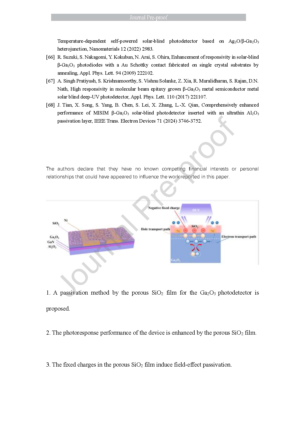
A passivation method by the porous SiO₂film for the Ga₂O₃ photodetector is proposed.
The photoresponse performance of the device is enhanced by the porous SiO₂film.
The fixed charges in the porous SiO₂film induce field-effect passivation.
Field-effect, chemical passivation and enhanced absorption improve devices.
Conclusion
In summary, we develop a surface passivation strategy employing sol-gel-derived porous SiO₂ films to enhance the photoresponse performance of Ga₂O₃ MSM solar-blind UV photodetectors. The introduction of the porous SiO₂ film accelerates the response speed, effectively reduces the dark current and enhances the photocurrent. Therefore, the detectivity and responsivity of the photodetector reaches 1.07 × 10¹³ Jones and 148.91 A/W at 30 V under 1.23 mW/cm² illumination, corresponding to 461% and 615% of those of the bare photodetector, respectively. Additionally, the photodetector maintains stable photoresponse after storage in atmospheric environment for 45 days. The porous SiO₂ film synergistically enhances the performance of the Ga₂O₃ photodetector through multiple effects: inducing field-effect passivation to suppress carrier recombination, improving photodetector stability via chemical passivation, and promoting enhanced light absorption through the porous structure. The surface passivation strategy based on the porous SiO₂ film offers a viable approach for the design and application of advancing ultra-wide bandgap semiconductor optoelectronic devices.
Project
This work was supported by the National Natural Science Foundation of China (Grant No. 62374076) and the Innovation/Entrepreneurship Program of Jiangsu Province (Grant No. JSSCTD202146).
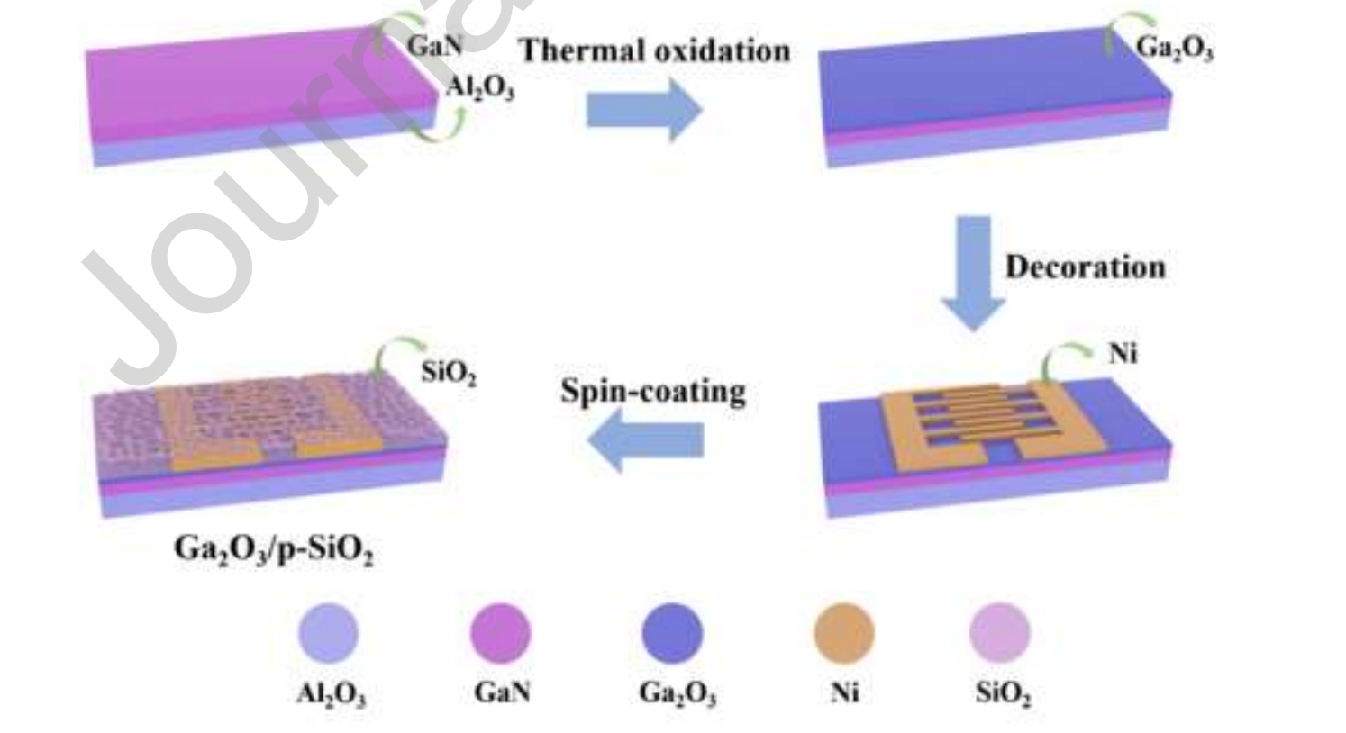
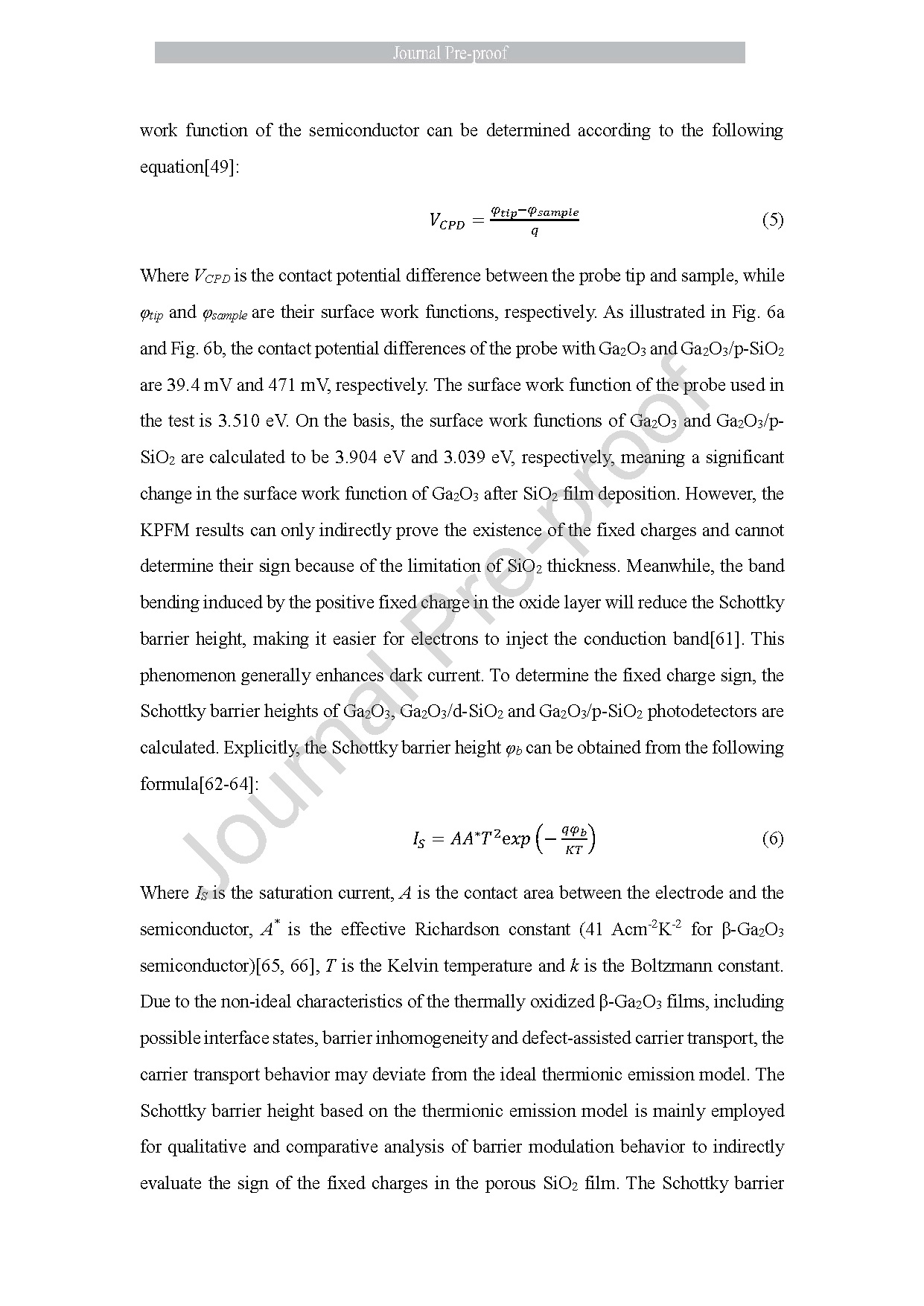
Fig. 1. Schematic diagram of the fabrication process of Ga₂O₃-based photodetectors.
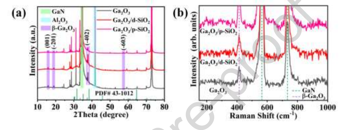
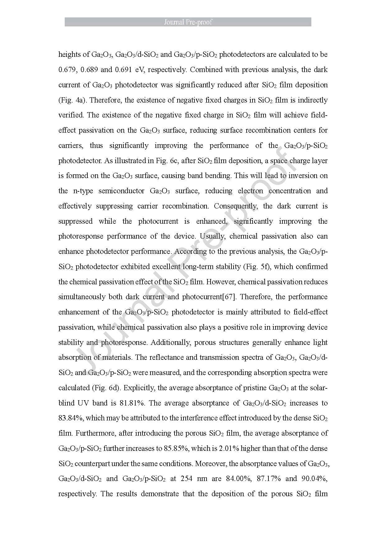
Fig. 2. (a) XRD patterns and (b) Raman spectra of Ga₂O₃, Ga₂O₃/d-SiO₂ and Ga₂O₃/p-SiO₂.
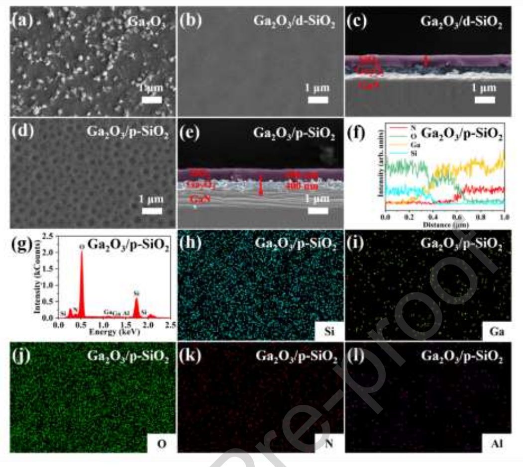
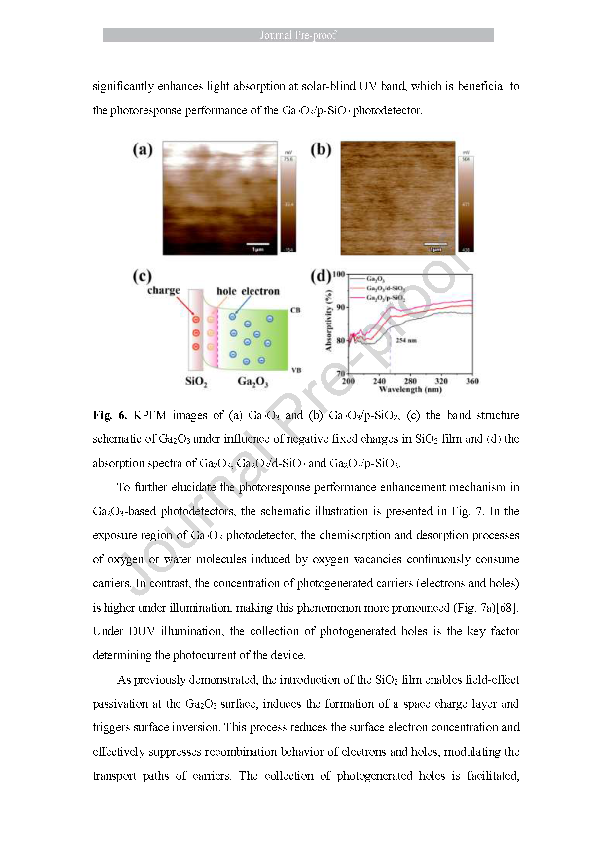
Fig. 3. (a) SEM image of Ga₂O₃, (b) SEM image and (c) cross-sectional SEM image of Ga₂O₃/d-SiO₂, (d) SEM image, (e) cross-sectional SEM image, (f) EDS line scan (along the red arrow), (g) EDS spectrum and (h-l) element mapping images of Ga₂O₃/p-SiO.
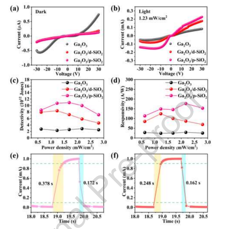
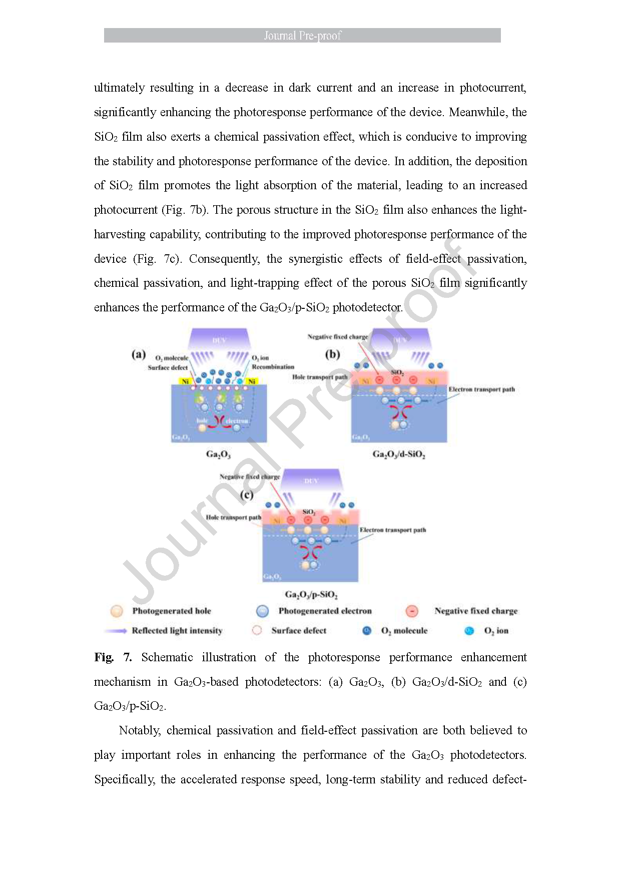
Fig. 4. I-V curves of Ga₂O₃, Ga₂O₃/d-SiO₂ and Ga₂O₃/p-SiO₂ photodetectors under (a) dark condition and (b) illumination condition, (c) detectivity and (d) responsivity curves of Ga₂O₃, Ga₂O₃/d-SiO₂ and Ga₂O₃/p-SiO₂ photodetectors under different light power densities, normalized I-t curves of (e) Ga₂O₃ and (f) Ga₂O₃/p-SiO₂ photodetectors.
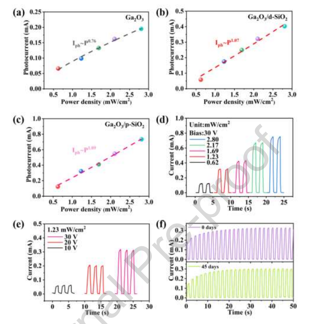
Fig. 5. Power-law fitting curve of photocurrent versus power density of (a) Ga₂O₃, (b) Ga₂O₃/d-SiO₂ and (c) Ga₂O₃/p-SiO₂ photodetectors, I-t curves under (d) different light power densities and (e) different bias voltages of Ga₂O₃/p-SiO₂ photodetector, (f) I-t curves of Ga₂O₃/p-SiO₂ photodetector before and after storage in ambient atmosphere for 45 days.
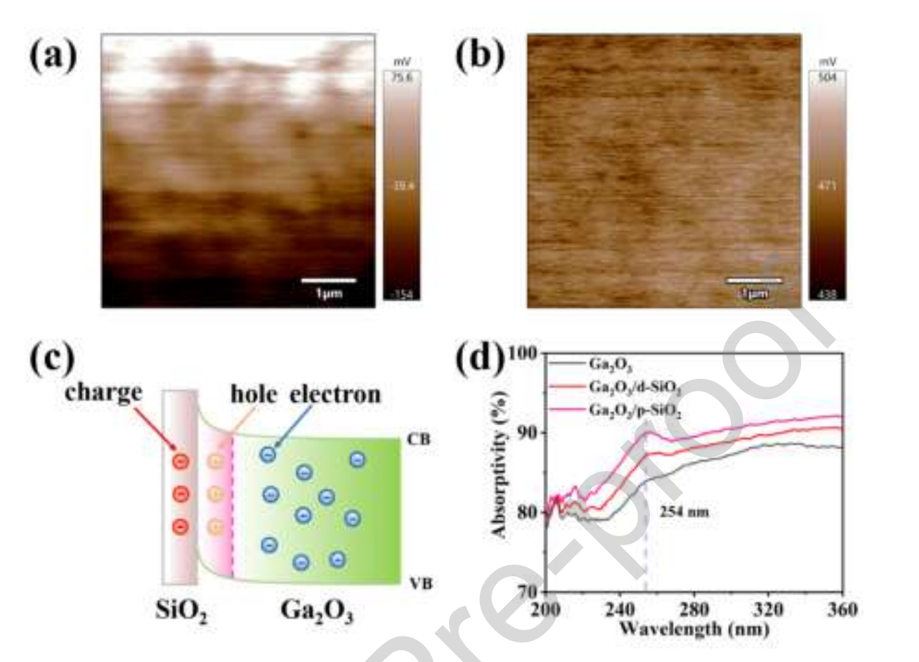
Fig. 6. KPFM images of (a) Ga₂O₃ and (b) Ga₂O₃/p-SiO₂ (c) the band structure schematic of Ga₂O₃ under influence of negative fixed charges in SiO₂ film and (d) the absorption spectra of Ga₂O₃, Ga₂O₃/d-SiO₂ and Ga₂O₃/p-SiO₂.
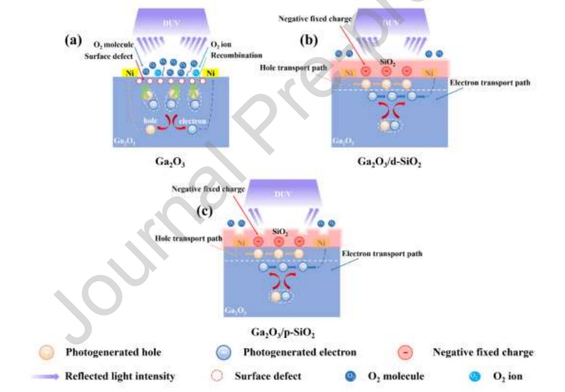
Fig. 7. Schematic illustration of the photoresponse performance enhancement mechanism in Ga₂O₃-based photodetectors: (a) Ga₂O₃, (b) Ga₂O₃/d-SiO₂ and (c) Ga₂O₃/p-SiO₂
DOI :
10.1016/j.jallcom.2026.189072

Instruction
Official Account

Cooperation
Top
