


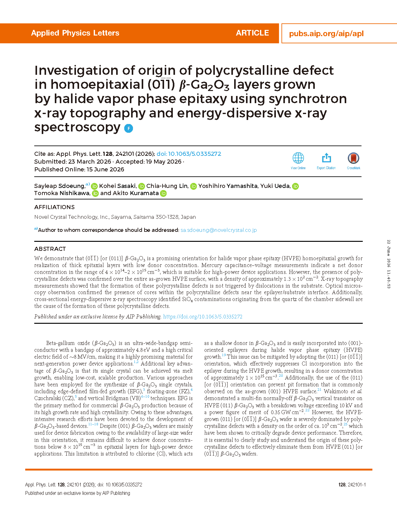
Researchers from the Novel Crystal Technology, Inc. have published a dissertation titled "Investigation of origin of polycrystalline defect in homoepitaxial (0-1-1) β-Ga₂O₃ layers grown by halide vapor phase epitaxy using synchrotron x-ray topography and energy-dispersive x-ray spectroscopy" in Applied Physics Letters.
Background
Beta-gallium oxide (β-Ga₂O₃) is an ultra-wide-bandgap semiconductor with a bandgap of ~4.8 eV and a critical electric field of 8 MV/cm, regarded as a promising candidate for next-generation power devices. Its single crystals can be fabricated via melt growth for low-cost mass production. At present, (001) β-Ga₂O₃ wafers dominate commercial device fabrication, yet chlorine shallow donors are readily incorporated into (001) epitaxial layers during HVPE growth, making it hard to reduce donor concentration below 8×10¹⁵ cm⁻³ and limiting high-voltage device performance.
The (0-1-1) orientation effectively suppresses Cl incorporation to achieve low donor concentration (~1×10¹⁵ cm⁻³) and eliminates surface pits typical of (001) HVPE films. Prior work realized vertical transistors with breakdown voltage over 10 kV on HVPE (0-1-1) β-Ga₂O₃. Nevertheless, HVPE-grown (0-1-1) epilayers suffer from pervasive polycrystalline defects with density of 10²–10³ cm⁻², which severely degrade device performance.
The root cause of such polycrystalline defects remains unclear; substrate dislocations and chamber contamination are suspected triggers. Besides, the (0-1-1) surface exhibits stronger anisotropic growth and inferior surface stability compared with (001), rendering it more vulnerable to local growth perturbations induced by foreign particles. This work adopts synchrotron X-ray topography, SEM and EDS to systematically uncover the origin of polycrystalline defects in HVPE (0-1-1) β-Ga₂O₃ homoepitaxial layers, laying theoretical foundation for defect elimination.
Abstract
We demonstrate that (0-1-1) β-Ga₂O₃ is a promising orientation for halide vapor phase epitaxy (HVPE) homoepitaxial growth for realization of thick epitaxial layers with low donor concentration. Mercury capacitance–voltage measurements indicate a net donor concentration in the range of 4 ×10¹⁴–2 ×10¹⁵ cm⁻³, which is suitable for high-power device applications. However, the presence of polycrystalline defects was confirmed over the entire as-grown HVPE surface, with a density of approximately 1.3 ×10² cm⁻². X-ray topography measurements showed that the formation of these polycrystalline defects is not triggered by dislocations in the substrate. Optical microscopy observation confirmed the presence of cores within the polycrystalline defects near the epilayer/substrate interface. Additionally, cross-sectional energy-dispersive x-ray spectroscopy identified SiOₓ contaminations originating from the quartz of he chamber sidewall are the cause of the formation of these polycrystalline defects.
Highlights
This work first traces the origin of polycrystalline defects in HVPE-grown (0-1-1) β-Ga₂O₃ homoepitaxial layers and excludes substrate dislocations as defect nucleation sources.
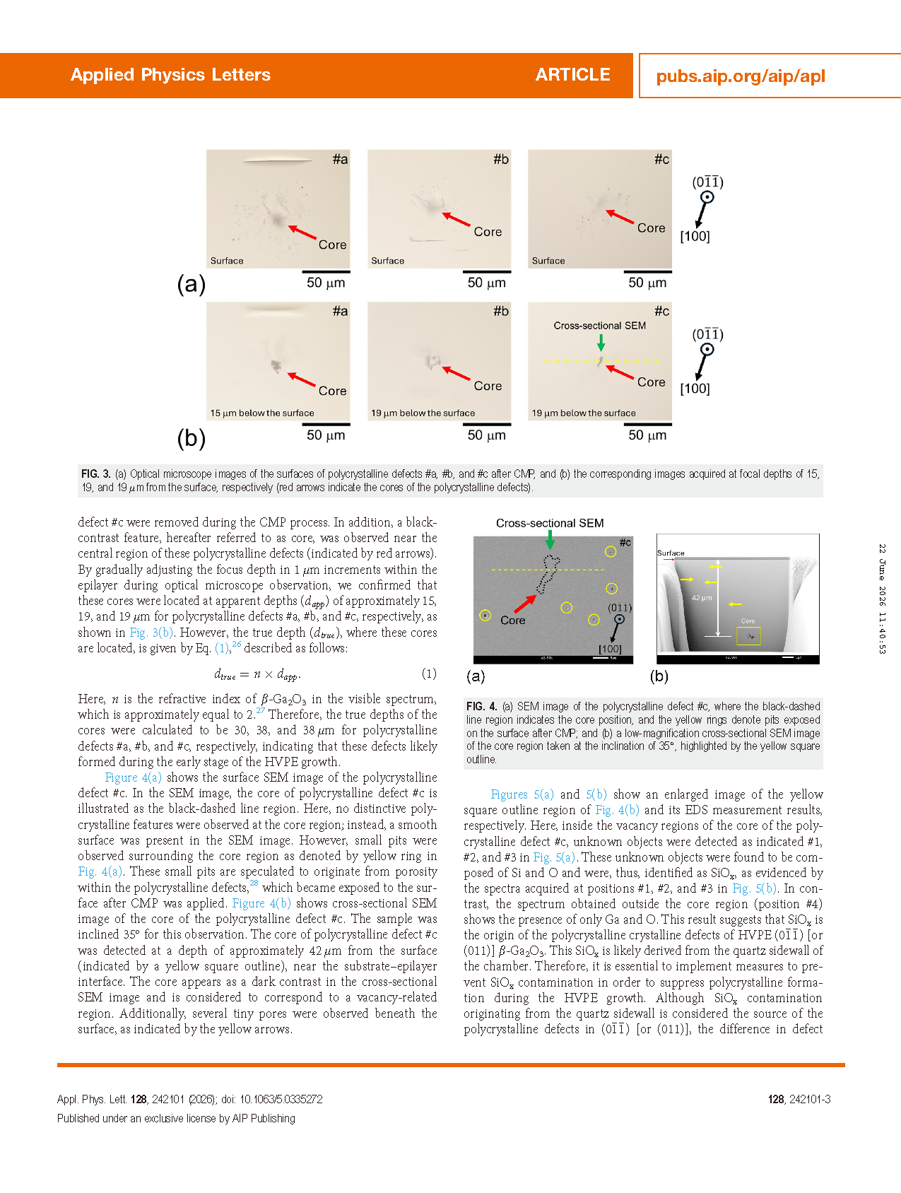
Combined confocal microscopy, cross-sectional SEM and depth-variable optical observation locate defect cores near the epilayer-substrate interface, verifying defects nucleate at the early HVPE growth stage.
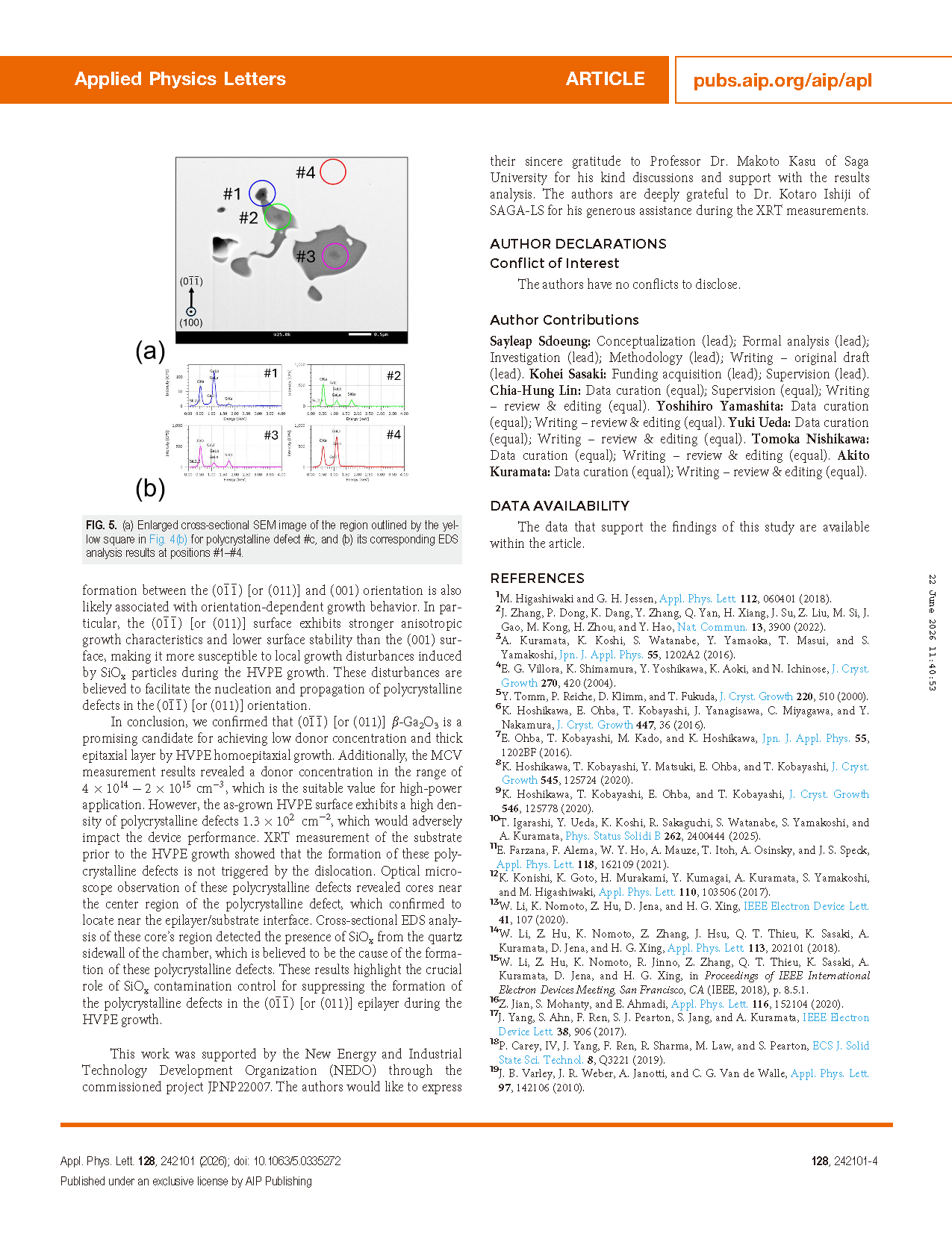
Cross-sectional EDS directly detects SiOₓ particles inside defect cores, confirming SiOₓ contamination released from chamber quartz sidewalls as the root cause of polycrystalline defects.
Reveals that (0-1-1) surface features stronger growth anisotropy and weaker surface stability than (001), which makes it more susceptible to polycrystalline nucleation triggered by SiOₓ particles, explaining orientation-dependent defect density discrepancy between (001) and (0-1-1).
Verifies HVPE (0-1-1) epilayers achieve ultra-low net donor concentration ranging from 4×10¹⁴ to 2×10¹⁵ cm⁻³, compatible with thick film growth and high-voltage power device requirements.
Conclusion
In conclusion, we confirmed that (0-1-1) β-Ga₂O₃ is a promising candidate for achieving low donor concentration and thick epitaxial layer by HVPE homoepitaxial growth. Additionally, the MCV measurement results revealed a donor concentration in the range of 4 ×10¹⁴–2 ×10¹⁵ cm⁻³, which is the suitable value for high-power application. However, the as-grown HVPE surface exhibits a high density of polycrystalline defects 1.3 ×10² cm⁻², which would adversely impact the device performance. XRT measurement of the substrate prior to the HVPE growth showed that the formation of these polycrystalline defects is not triggered by the dislocation. Optical microscope observation of these polycrystalline defects revealed cores near the center region of the polycrystalline defect, which confirmed to locate near the epilayer/substrate interface. Cross-sectional EDS analysis of these core’s region detected the presence of SiOₓ from the quartz sidewall of the chamber, which is believed to be the cause of the formation of these polycrystalline defects. These results highlight the crucial SiOₓ contamination control for suppressing the formation of the polycrystalline defects in the (0-1-1) epilayer during the HVPE growth.
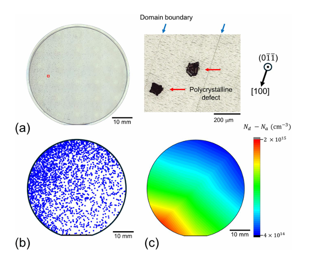
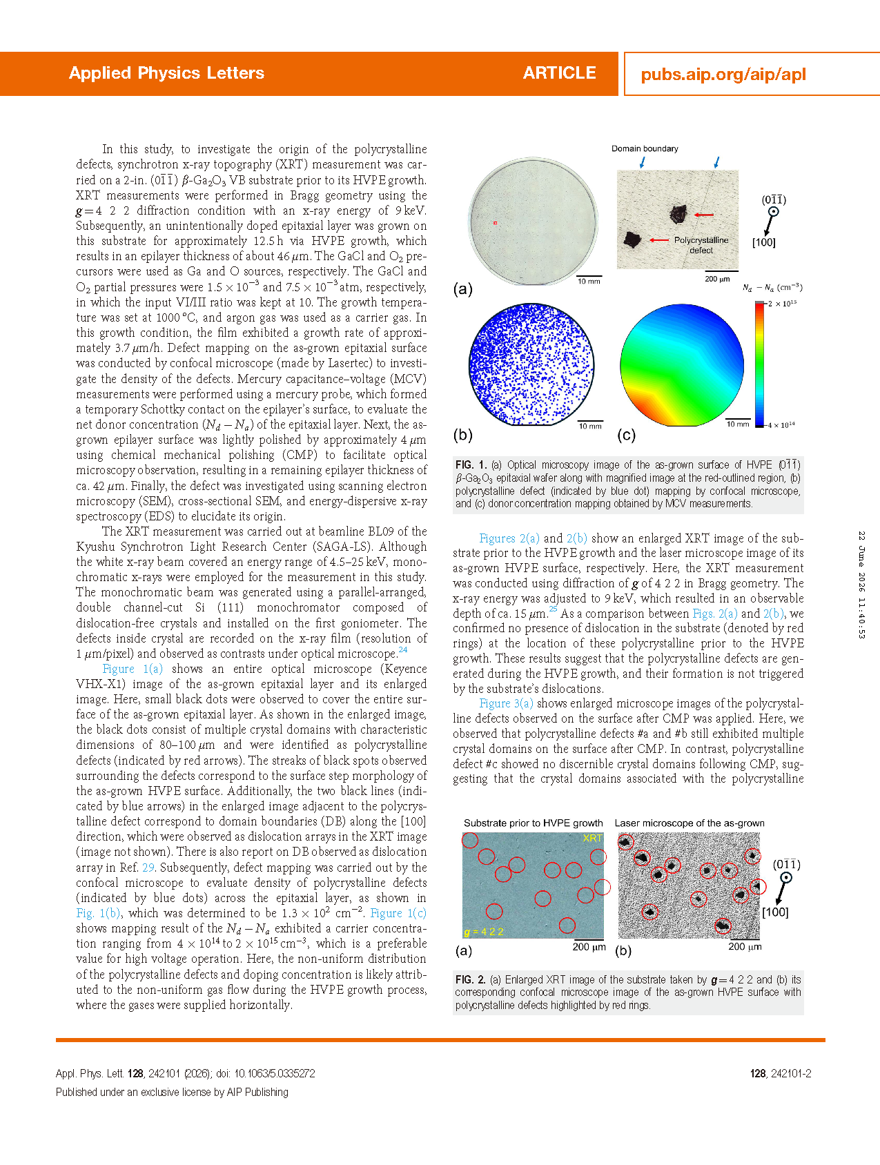
Figure 1. (a) Optical microscopy image of the as-grown surface of HVPE (0-1-1) β-Ga₂O₃ epitaxial wafer along with magnified image at the red-outlined region, (b) polycrystalline defect (indicated by blue dot) mapping by confocal microscope, and (c) donor concentration mapping obtained by MCV measurements.
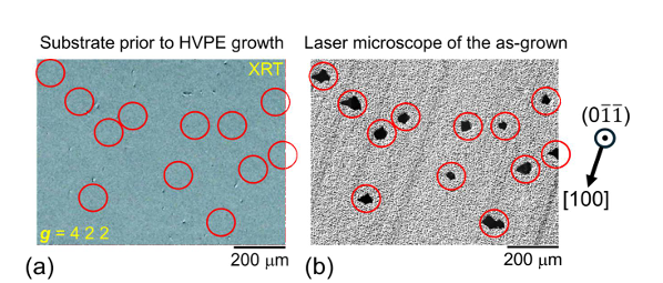
Figure 2. (a) Enlarged XRT image of the substrate taken by g=4 2 2 and (b) its corresponding confocal microscope image of the as-grown HVPE surface with polycrystalline defects highlighted by red rings.
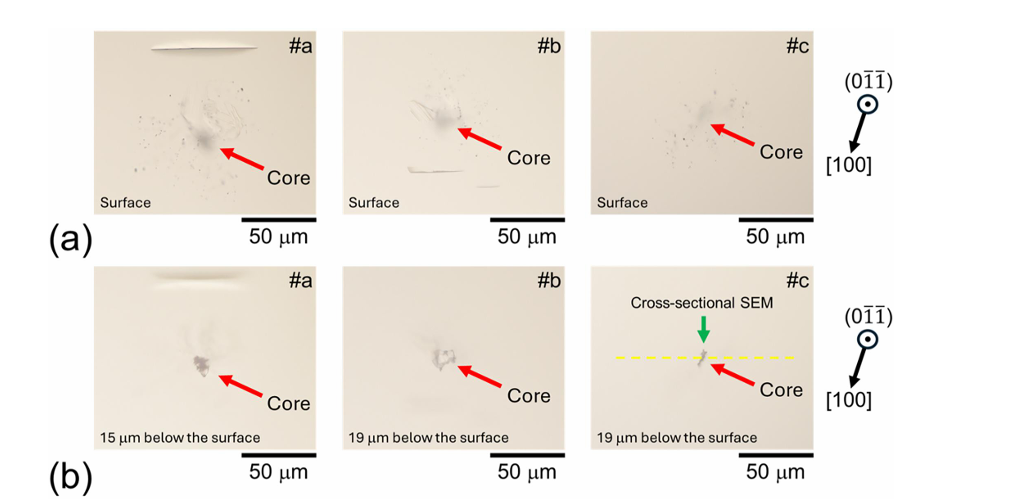
Figure 3. (a) Optical microscope images of the surfaces of polycrystalline defects #a, #b, and #c after CMP, and (b) the corresponding images acquired at focal depths of 15, 19, and 19 μm from the surface, respectively (red arrows indicate the cores of the polycrystalline defects).
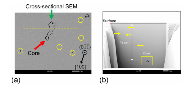
Figure 4. (a) SEM image of the polycrystalline defect #c, where the black-dashed line region indicates the core position, and the yellow rings denote pits exposed on the surface after CMP; and (b) a low-magnification cross-sectional SEM image of the core region taken at the inclination of 35°, highlighted by the yellow square outline.
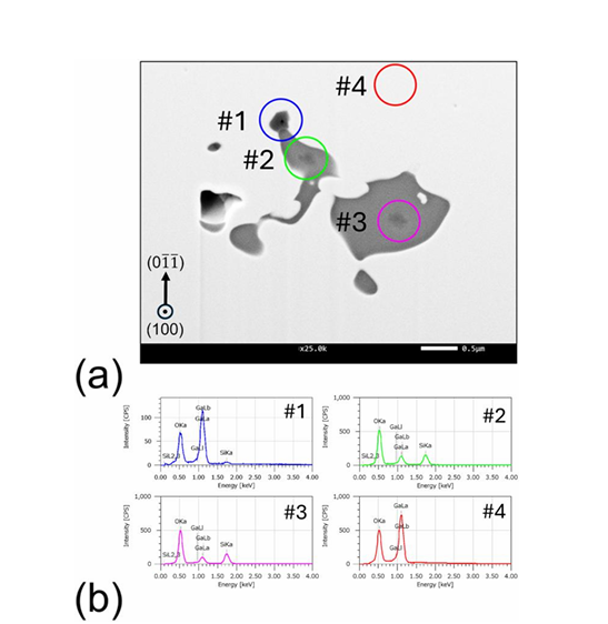
Figure 5. (a) Enlarged cross-sectional SEM image of the region outlined by the yellow square in Fig. 4(b) for polycrystalline defect #c, and (b) its corresponding EDS analysis results at positions #1–#4.
DOI:
10.1063/5.0335272

Instruction
Official Account

Cooperation
Top
