


Researchers from the University of Science and Technology of China and National University of Singapore have published a dissertation titled "Over 2.5 GW/cm² Vertical β-Ga₂O₃ Schottky Barrier Diode with High-k Field Plate and Multi Zone Gradient Rings Assisted JTE" in 2026 IEEE 38th International Symposium on Power Semiconductor Devices and ICs (ISPSD).
Background
Power electronic devices are core components of energy conversion systems. Improving device efficiency and power density is critical for large-scale electrification and carbon emission reduction. As an ultra-wide bandgap semiconductor, β-Ga₂O₃ features an ultra-wide bandgap of ~4.8 eV and an ultrahigh critical electric field of ~8 MV/cm with controllable n-type doping. Large-area wafers can be manufactured via melt-growth technology, making β-Ga₂O₃ a promising candidate for next-generation high-voltage low-loss power devices.
High-performance edge termination is essential to fully utilize the high breakdown voltage property of β-Ga₂O₃. Conventional termination technologies have obvious limitations: single-zone JTE is extremely sensitive to p-NiO doping concentration with a narrow process window; non-embedded field limiting rings (FLR) have weak electric field modulation capability, while embedded FLR requires etching that causes interface damage and degrades forward characteristics and long-term reliability; traditional multi-zone JTE requires repeated photolithography and sputtering, increasing manufacturing cost and process complexity.
This work proposes a composite BMR-JTE termination combining high-k BaTiO₃ field plate and multi-zone gradient rings without any etching steps. The high-k dielectric extends surface depletion regions via polarization effect and fully activates non-embedded FLRs to homogenize peripheral electric field. The linearly variable ring spacing weakens abrupt charge change in termination and greatly broadens the doping tolerance window of JTE. Without sacrificing forward conduction performance, the device achieves ultra-high breakdown voltage and ultra-low specific on-resistance with outstanding thermal stability, offering a low-cost and highly reliable termination solution for multi-kilovolt β-Ga₂O₃ power devices.
Abstract
This work presents a vertical β-Ga₂O₃ Schottky barrier diode (SBD) featuring a high-k BaTiO₃ field plate (FP) and multi-zone gradient rings assisted junction termination extension (BMR-JTE). The BMR-JTE SBD integrates the high-k FP to enhance lateral depletion and activate nonembedded field limiting ring (FLR), thereby alleviating the surface electric field crowding effectively. The fabricated BMR-JTE SBD achieves a high breakdown voltage of 3331 V with a low specific on-resistance of 4.33 mΩ·cm², resulting in a power figure of merit (PFOM) of 2.56 GW/cm². In addition, the device exhibits robust high-temperature performance, sustaining a breakdown voltage exceeding 2100 V at 448 K. The BMR-JTE termination is realized through a simple fabrication process without etching damage, demonstrating a highly competitive termination strategy for multi-kilovolt class β-Ga₂O₃ power devices.
Highlights
A novel composite termination structure integrating high-k BaTiO₃field plate and 3-zone gradient p-NiO FLR assisted JTE is proposed. No etching steps are required during fabrication to completely eliminate semiconductor interface damage caused by etching;
The polarization effect of high-k BTO dielectric broadens surface depletion regions and fully activates non-embedded FLRs, significantly reducing peak electric field at device edge, with breakdown voltage improved by 56% compared with conventional single-zone JTE;
Linear gradient ring spacing design achieves gradual equivalent p-type charge distribution in termination region for uniform electric field. Simulation and experimental results verify the optimal gradient A=0.6 μm and first zone ring spacing S₁=3 μm, realizing a breakdown voltage up to 3331 V;
The structure drastically broadens the p-type doping window of JTE, maintaining low peak electric field within a wide doping range from 1×10¹⁷to 2×10¹⁹ cm⁻³, solving the industrial bottleneck of doping sensitivity and difficult mass production of traditional JTE;
The device achieves state-of-the-art performance with a PFOM of 2.56 GW/cm², retains breakdown voltage over 2100 V at 448 K, and its forward conduction characteristics are not degraded by the termination structure.
Conclusion
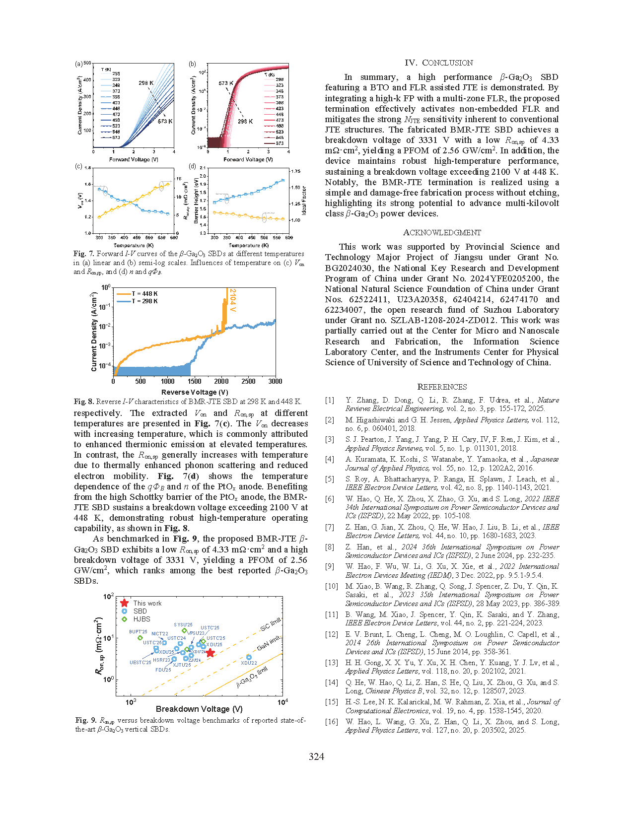
In summary, a high performance β-Ga₂O₃ SBD featuring a BTO and FLR assisted JTE is demonstrated. By integrating a high-k FP with a multi-zone FLR, the proposed termination effectively activates non-embedded FLR and mitigates the strong N_JTE sensitivity inherent to conventional JTE structures. The fabricated BMR-JTE SBD achieves a breakdown voltage of 3331 V with a low Ron,sp of 4.33 mΩ·cm², yielding a PFOM of 2.56 GW/cm². In addition, the device maintains robust high-temperature performance, sustaining a breakdown voltage exceeding 2100 V at 448 K. Notably, the BMR-JTE termination is realized using a simple and damage-free fabrication process without etching, highlighting its strong potential to advance multi-kilovolt class β-Ga₂O₃ power devices.
Project Support
This work was supported by Provincial Science and Technology Major Project of Jiangsu under Grant No. BG2024030, the National Key Research and Development Program of China under Grant No. 2024YFE0205200, the National Natural Science Foundation of China under Grant Nos. 62522411, U23A20358, 62404214, 62474170 and 62234007, the open research fund of Suzhou Laboratory under Grant no. SZLAB-1208-2024-ZD012. This work was partially carried out at the Center for Micro and Nanoscale Research and Fabrication, the Information Science Laboratory Center, and the Instruments Center for Physical Science of University of Science and Technology of China.
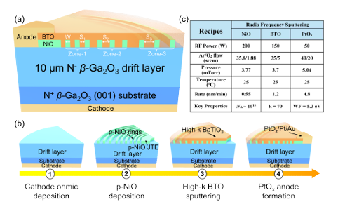
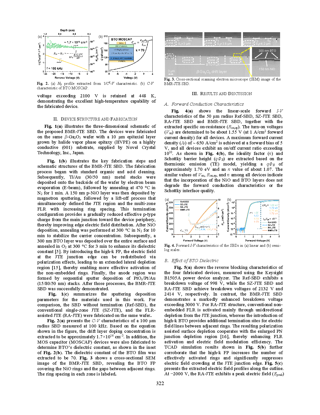
Figure 1 (a) The 3D schematic view of the BMR-JTE SBD. (b) The recipe parameters of the sputtering materials used in this work. (c) The key fabrication process flow of the BMR-JTE SBD.
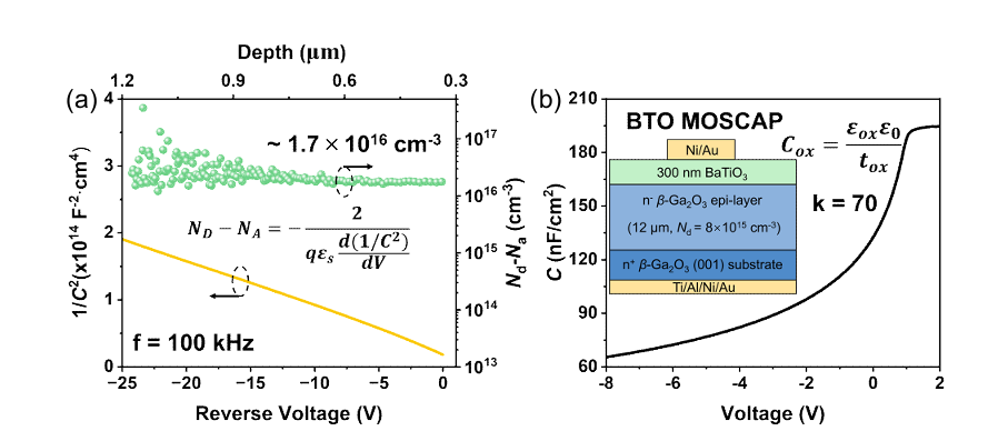
Figure 2 (a) ND profile extracted from 1/C²-V characteristic. (b) C-V characteristic of BTO MOSCAP.
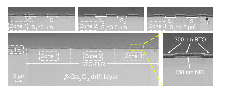
Figure 3 Cross-sectional scanning electron microscope (SEM) image of the BMR-JTE SBD.
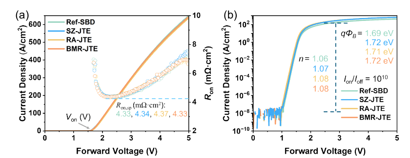
Figure 4 Forward I-V characteristics of the SBDs in (a) linear and (b) semilog scales.
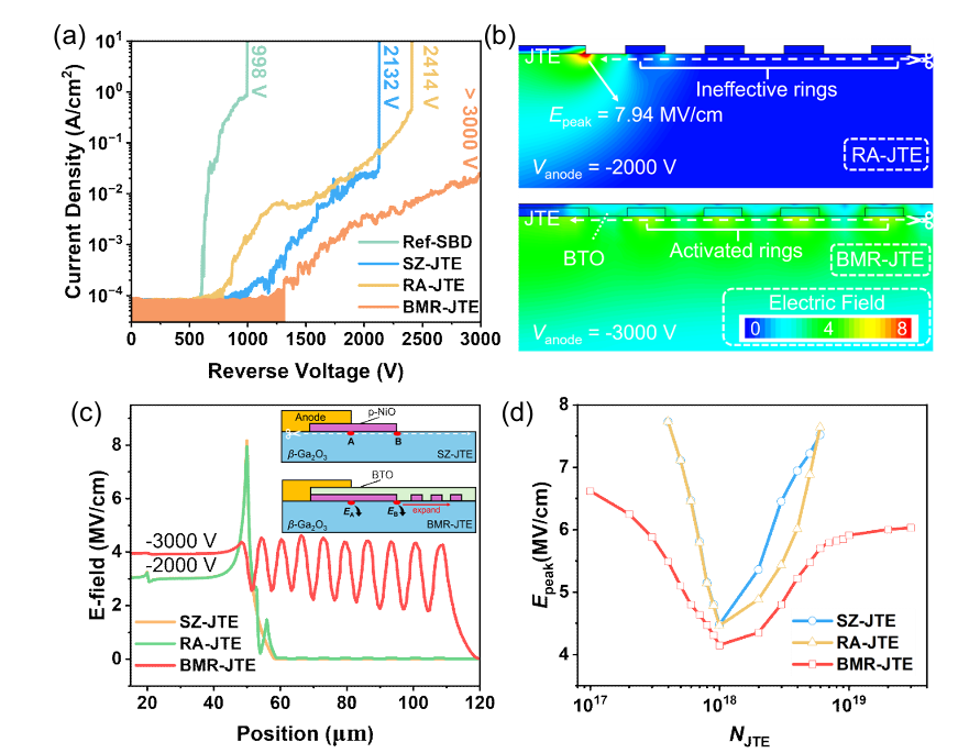
Figure 5 (a) Comparison of the reverse I-V characteristics of Ref-SBD, SZ-JTE, RA-JTE, and BMR-JTE. (b) Simulated E-field distribution of RA-JTE and BMR-JTE. (c) Comparison of E-field profiles of SZ-JTE, RA-JTE, and BMR-JTE under −2000 V, −2000 V, and −3000 V. (d) Simulated Epeak versus NJTE of the SBDs under −2500 V. Inset in (c): schematic comparison of potential Epeak locations in SZ-JTE and BMR-JTE.
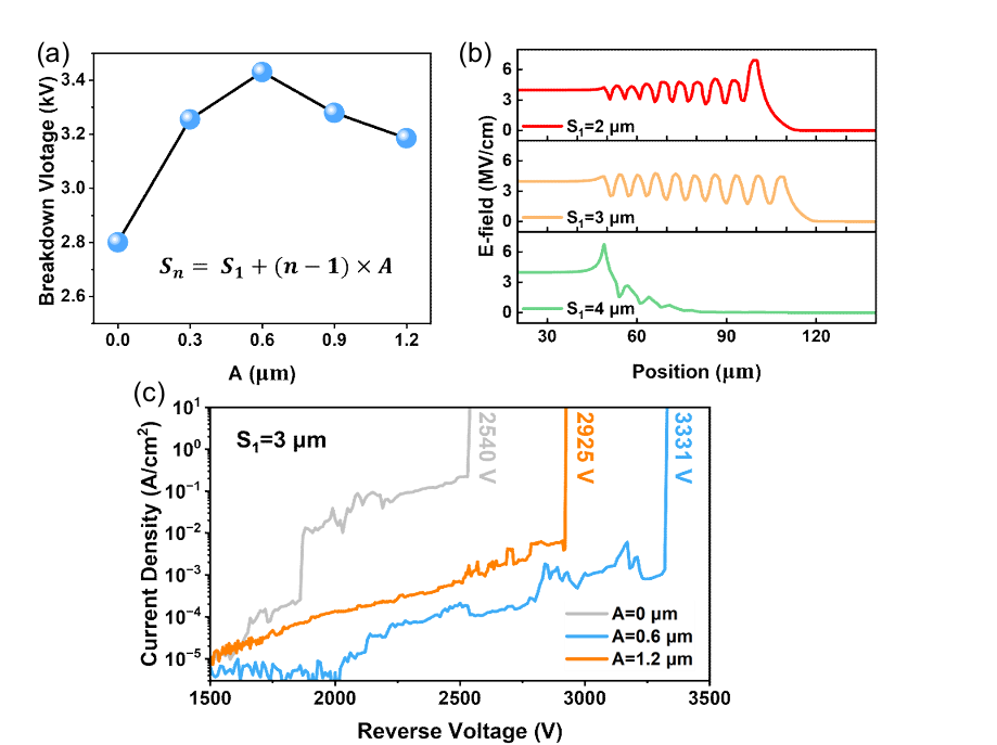
Figure 6 (a) Simulated breakdown versus A. (b) E-field distributions along the surface of the BMR-JTE SBD with different S₁. (c) Comparison of the reverse I-V characteristics of BMR-JTE SBD with different A.
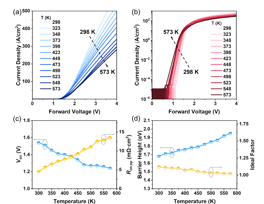
Figure 7 (a)(b) Forward I-V curves of the β-Ga₂O₃ SBDs at different temperatures in linear and semi-log scales. (c) Influences of temperature on Von and Ron,sp. (d) Influences of temperature on n and qΦB.
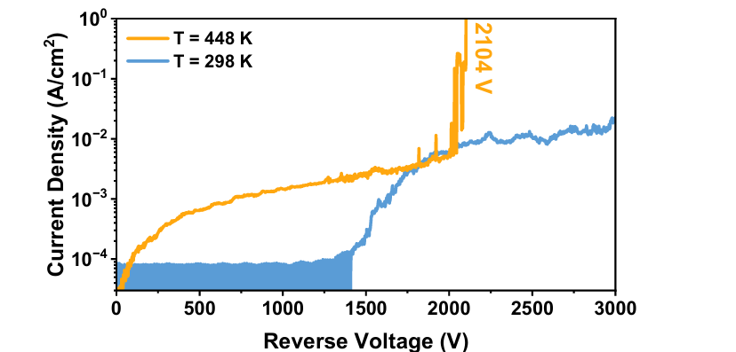
Figure 8 Reverse I-V characteristics of BMR-JTE SBD at 298 K and 448 K.
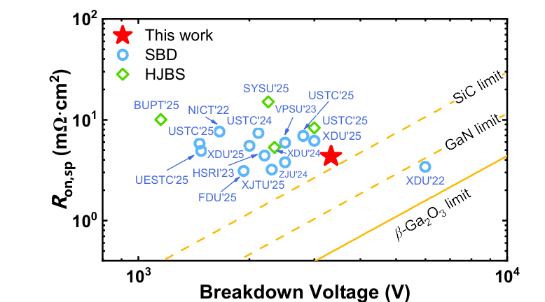
Figure 9 Ron,sp versus breakdown voltage benchmarks of reported state-of-the-art β-Ga₂O₃ vertical SBDs.
DOI:
10.1109/ISPSD64561.2026.11553726
Instruction
Official Account

Cooperation
Top
