


Researchers from the Beijing National Laboratory for Condensed Matter Physics, Institute of Physics, Chinese Academy of Sciences & School of Integrated Circuits, Beijing University of Posts and Telecommunications have published a paper titled "Irradiation-Induced Performance Degradation of β-Ga₂O₃ Crystals and Schottky Barrier Diodes: Proton vs Neutron" in Chinese Physics B.
Background
In the space environment, electronic devices are exposed to energetic particles and ionizing radiation, which can induce degradation of device performance and consequently compromise the reliability of spacecraft in orbit. This necessitates the development of electronic materials with high resistance to space radiation. As a fourth-generation ultra-wide bandgap semiconductor, gallium oxide (Ga₂O₃) exhibits a wide bandgap, a high breakdown electric field, and a superior Baliga’s figure of merit, which are critical parameters for high-power, high-voltage, and radiation-tolerant electronic technologies.
β-Ga₂O₃ is the most thermodynamically stable phase of gallium oxide, and its bulk single crystals can be fabricated via low-cost melt growth methods represented by EFG technique, showing great commercialization potential for power electronics and space photoconductive devices. In aerospace and nuclear service environments, devices will be bombarded by protons, neutrons and other high-energy particles, generating lattice vacancy defects and carrier depletion, severely damaging device electrical properties.
Existing researches have separately studied proton or neutron irradiation damage of β-Ga₂O₃, but systematic comparative experiments based on identical irradiation parameters on EFG-grown (100) Sn-doped β-Ga₂O₃ single crystals are scarce. Few studies establish direct correlation between lattice disorder degree and Schottky diode electrical degradation mechanism, which restricts the application of β-Ga₂O₃ in radiation-resistant electronic devices.
Abstract
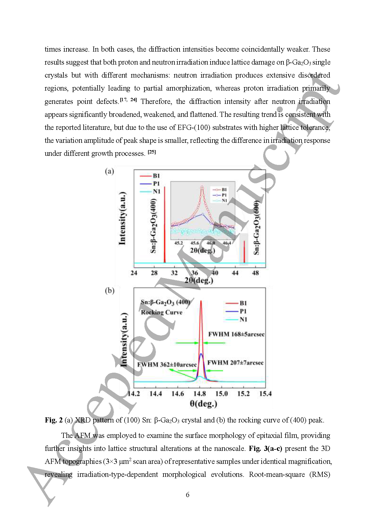
Radiation-tolerant wide-bandgap semiconductors are essential for high-performance electronic devices in space and nuclear environments. Here, (100)-oriented Sn-doped β-Ga₂O₃ single crystals were used to systematically investigate defect evolution under 100 MeV proton and neutron irradiation with a fluence of 1 ×10¹² cm⁻². Schottky contacts were fabricated to characterize the resultant electrical performance degradation after irradiation. X-ray diffraction results show that both pristine and irradiated samples preserve the (100) preferential orientation. Proton irradiation causes negligible lattice disorder with an increment below 1%, while neutron irradiation leads to severe displacement damage, as evidenced by a roughly 2.15-fold increase in the XRD peak full-width at half-maximum. Electrical tests on Schottky contacts present distinct characteristics for two irradiation sources. After proton irradiation, the devices keep a forward/reverse current ratio over 10⁶, low on-resistance of 6 mΩ·cm², showing outstanding resistance to proton radiation. For neutron-irradiated samples, obvious lattice defects are generated, yet the devices still possess favorable rectification performance with I_on / I_off >10⁵. Under equivalent fluences, β-Ga₂O₃ exhibits better radiation resistance than SiC and GaN. This study establishes a clear defect-material properties correlation: proton-induced point defects exhibit efficient dynamic annealing, while neutron-generated defect clusters (via displacement cascades) persist, dominating device degradation. These findings provide critical metrics for β-Ga₂O₃ in space/nuclear applications and offer guidance for the design of radiation-mitigation strategies in wide-bandgap semiconductors.
Highlights
First comparative study on EFG-grown (100) Sn-doped β-Ga₂O₃under identical 100 MeV proton and neutron irradiation (fluence 1×10¹² cm⁻²).
Reveal completely different damage mechanisms: proton induces shallow surface point defects with dynamic annealing; neutron triggers bulk cascaded displacement damage and stable defect clusters.
Construct a multi-dimensional characterization system combining XRD, AFM, XPS, PL, UV-Vis and semiconductor electrical test to link lattice defects, surface morphology, chemical bonding and device electrical degradation.
Quantitatively compare radiation resistance of β-Ga₂O₃, SiC and GaN, verify ultra-high proton radiation tolerance of β-Ga₂O₃Schottky diodes.
Provide quantitative structural & electrical parameters and damage mechanism support for space/nuclear radiation-resistant β-Ga₂O₃ power device design.
Conclusion
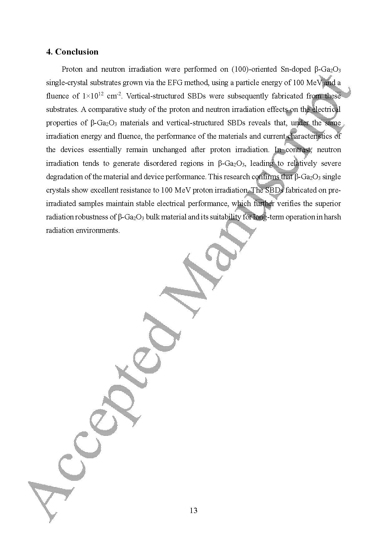
Proton and neutron irradiation were performed on (100)-oriented Sn-doped β-Ga₂O₃ single-crystal substrates grown via the EFG method, using a particle energy of 100 MeV and a fluence of 1 ×10¹² cm⁻². Vertical-structured SBDs were subsequently fabricated from these substrates. A comparative study of the proton and neutron irradiation effects on the electrical properties of β-Ga₂O₃ materials and vertical-structured SBDs reveals that, under the same irradiation energy and fluence, the performance of the materials and current characteristics of the devices essentially remain unchanged after proton irradiation. In contrast, neutron irradiation tends to generate disordered regions in β-Ga₂O₃, leading to relatively severe degradation of the material and device performance. This research confirms that β-Ga₂O₃ single crystals show excellent resistance to 100 MeV proton irradiation. The SBDs fabricated on preirradiated samples maintain stable electrical performance, which further verifies the superior radiation robustness of β-Ga₂O₃ bulk material and its suitability for long-term operation in harsh radiation environments.
Project Support
This work was financially supported by the National Natural Science Foundation of China (Grant No. 52572146).
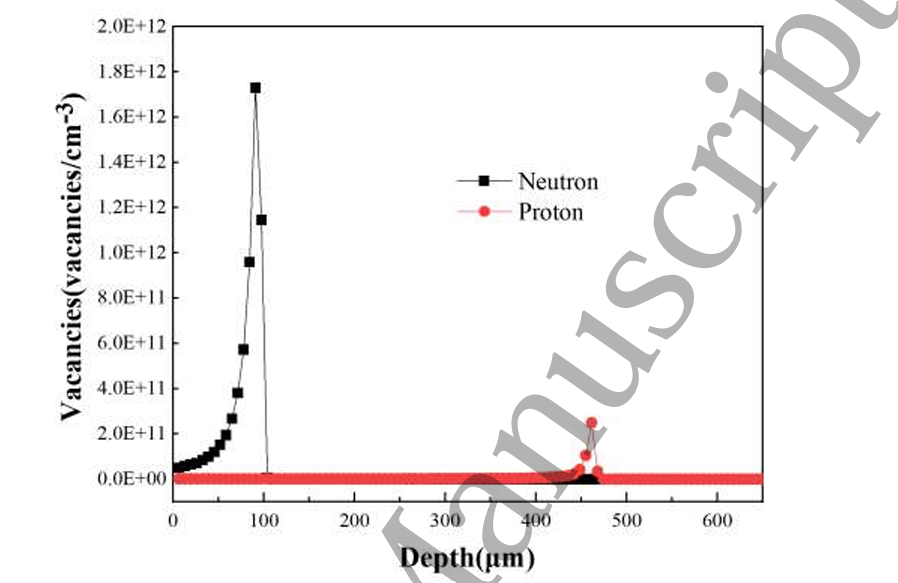
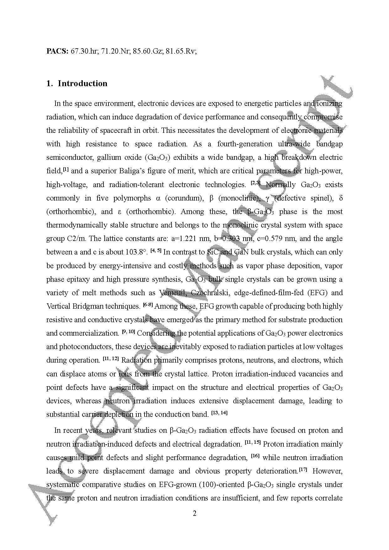
Figure 1 Vacancy concentration depth distribution induced by proton and neutron irradiation in β-Ga₂O₃
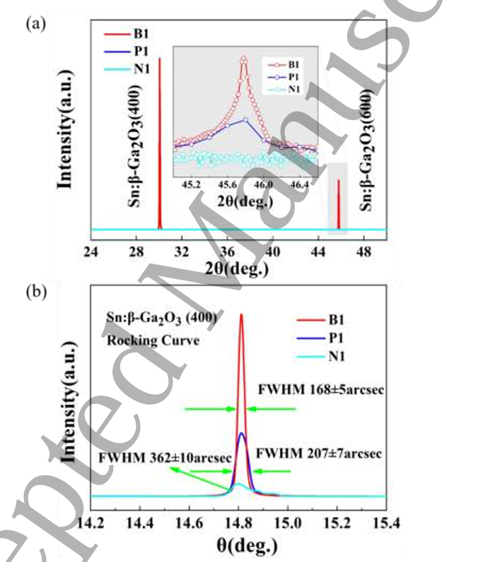
Figure 2 (a) XRD 2θ-ω pattern of pristine & irradiated Sn: β-Ga₂O₃ crystal; (b) (400) diffraction rocking curve
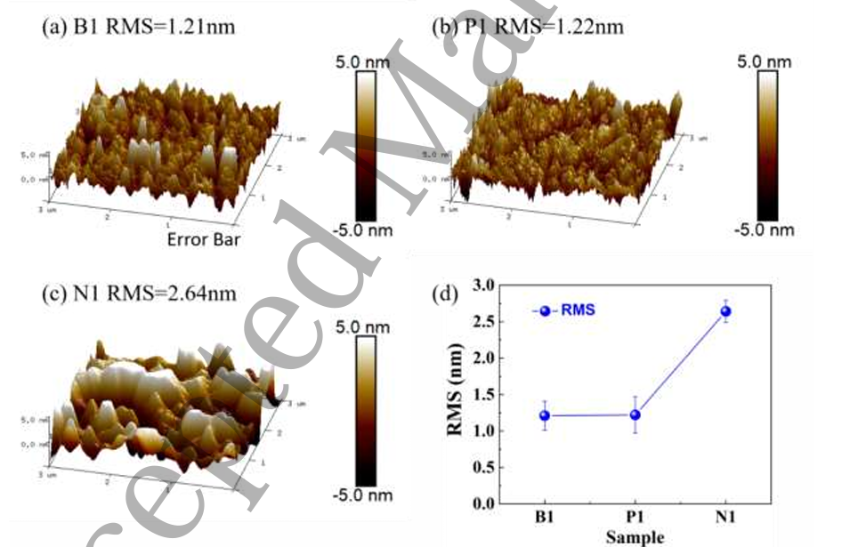
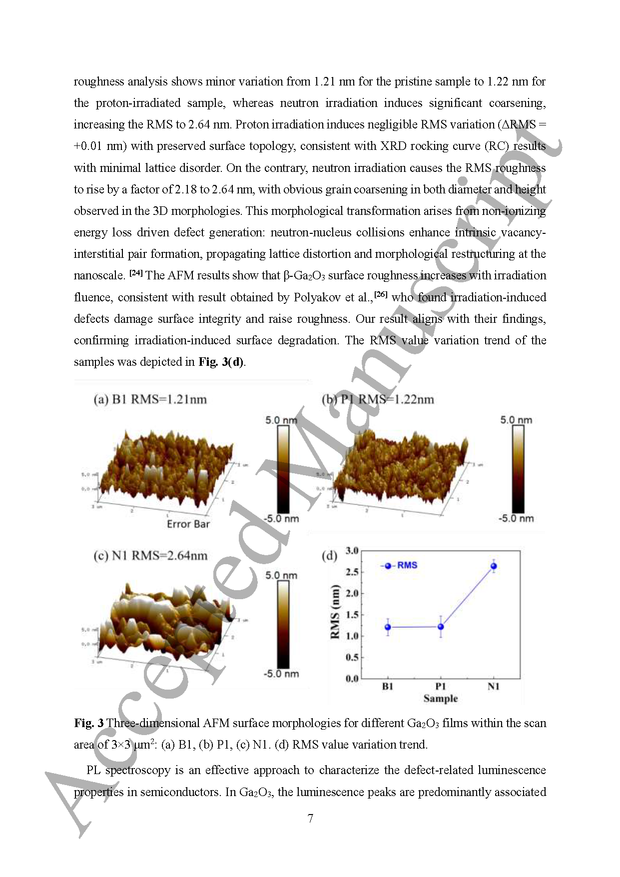
Figure 3 (a-c) 3D AFM surface topography of B1/P1/N1 samples (3×3 μm² scan); (d) RMS roughness variation trend
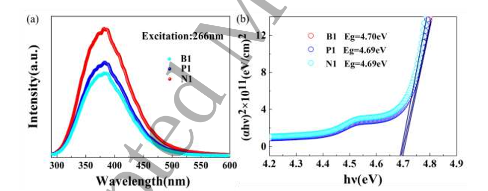
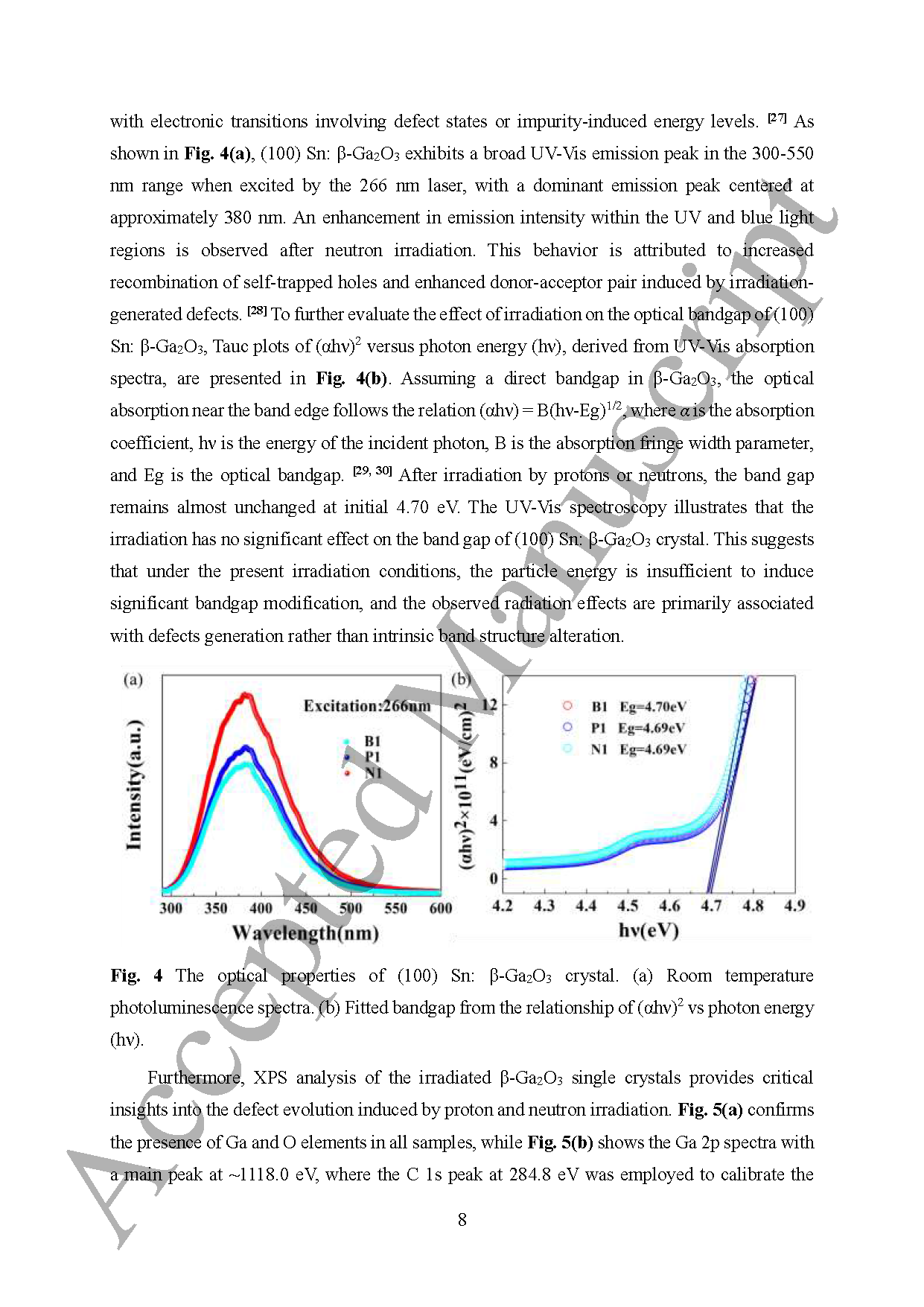
Figure 4 Optical characterization of Sn: β-Ga₂O₃: (a) room-temperature PL spectra; (b) (αhν)²-hν bandgap fitting curve
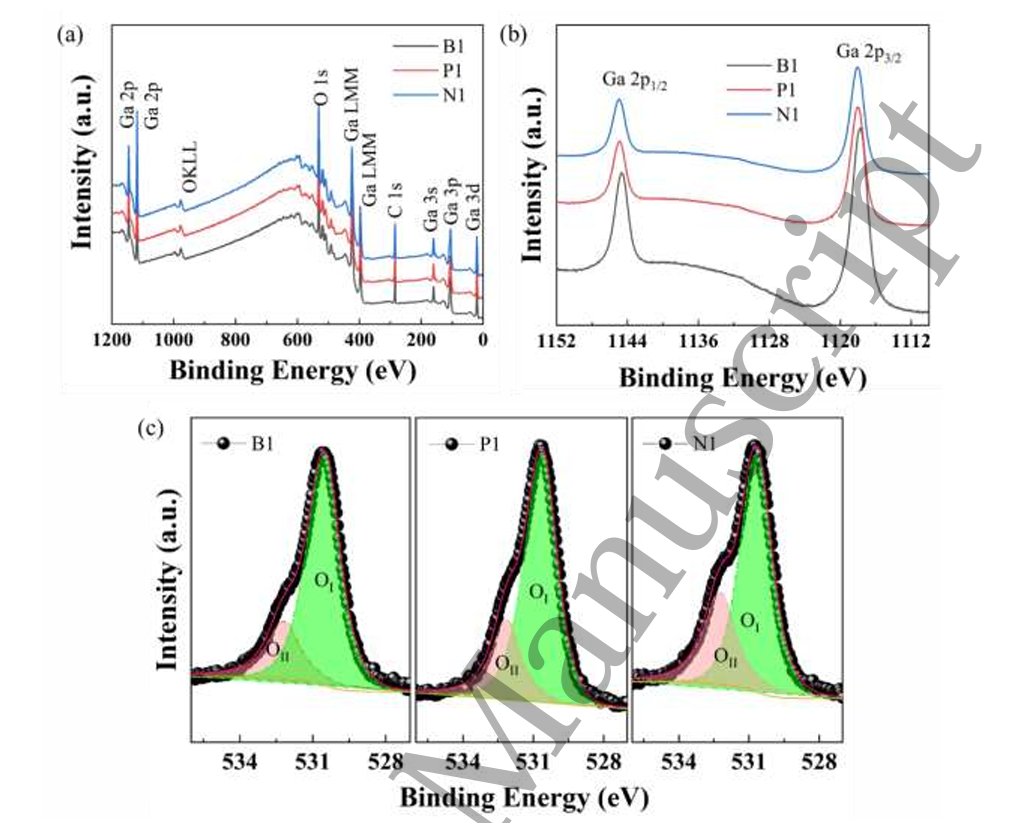
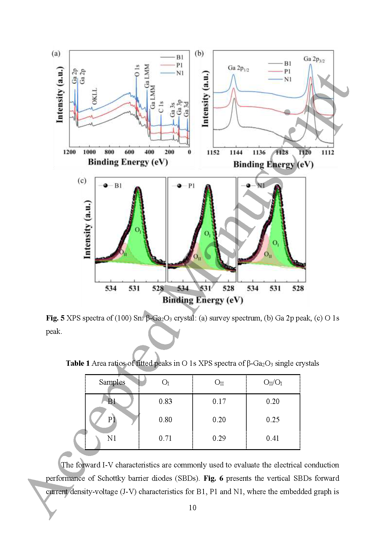
Figure 5 XPS full spectrum and core-level spectra of Sn: β-Ga₂O₃: (a) survey spectrum; (b) Ga 2p core peak; (c) deconvoluted O 1s peak
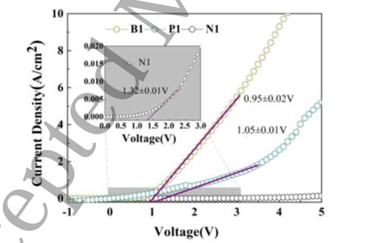
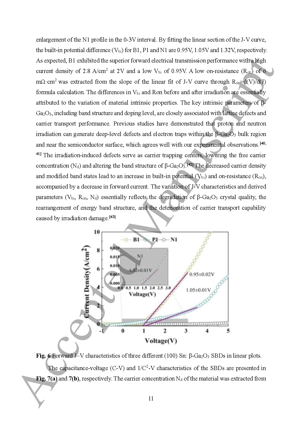
Figure 6 Forward J-V characteristic curves of three β-Ga₂O₃ vertical Schottky barrier diodes
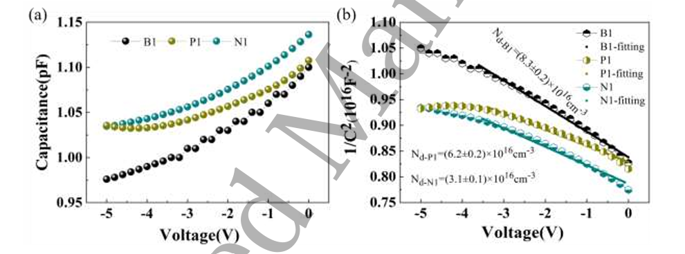
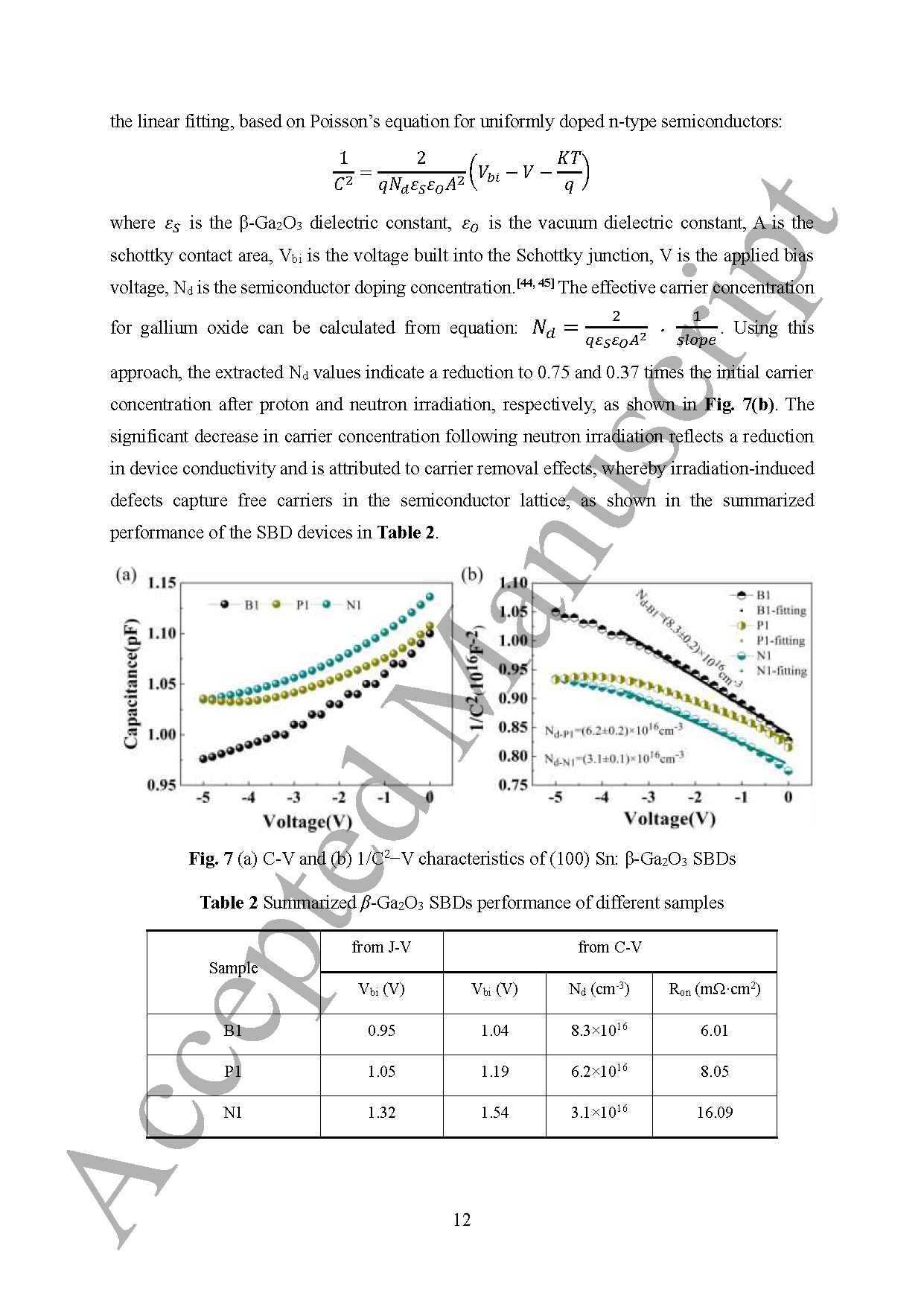
Figure 7 Electrical capacitance characterization: (a) C-V curves of SBDs; (b) 1/C²-V fitting curves for carrier concentration extraction
DOI:
doi.org/10.1088/1674-1056/ae7e73

Instruction
Official Account

Cooperation
Top
