


What Does Doping Change in Materials?
Doping refers to the introduction of a small amount of foreign atoms into a host material, where the dopant atoms either substitute for the original lattice atoms or occupy interstitial sites. Because dopant atoms usually differ from host atoms in terms of atomic radius, valence state, electronegativity, and electronic configuration, their incorporation into the lattice can trigger a series of interconnected changes within the material.
Rather than simply stating that “doping improves material performance,” analyzing the specific aspects altered by doping provides a deeper understanding of its underlying mechanisms. The dominant effects of doping vary across different material systems: in some cases, doping primarily regulates electrical conductivity, while in others it mainly modifies properties such as light absorption or catalytic activity. These differences fundamentally arise from the compatibility between the dopant element and the host material, as well as the extent to which different structural levels are affected.
From the perspective of structural hierarchy—from macroscopic structure to microscopic electronic properties, and from cause to effect—the changes induced by doping can generally be categorized into five aspects: lattice geometry (such as lattice constants and unit cell volume), local structures around dopant atoms (such as bond lengths and coordination environments), electronic structure (such as band structure and density of states), valence states and carrier distribution, and ultimately macroscopic properties such as bandgap and optical behavior.
These five types of changes are not independent but instead form a continuous causal chain. The mismatch in atomic size and charge between dopants and host atoms first induces lattice distortion and local bond rearrangement, which subsequently leads to the redistribution of electronic structures and valence states. These microscopic changes are ultimately reflected in macroscopic properties, including bandgap variation, electrical conductivity, and optical absorption characteristics.
The following sections will follow this logical framework, examining each level of change step by step and discussing the corresponding characterization techniques used to analyze and verify these effects.
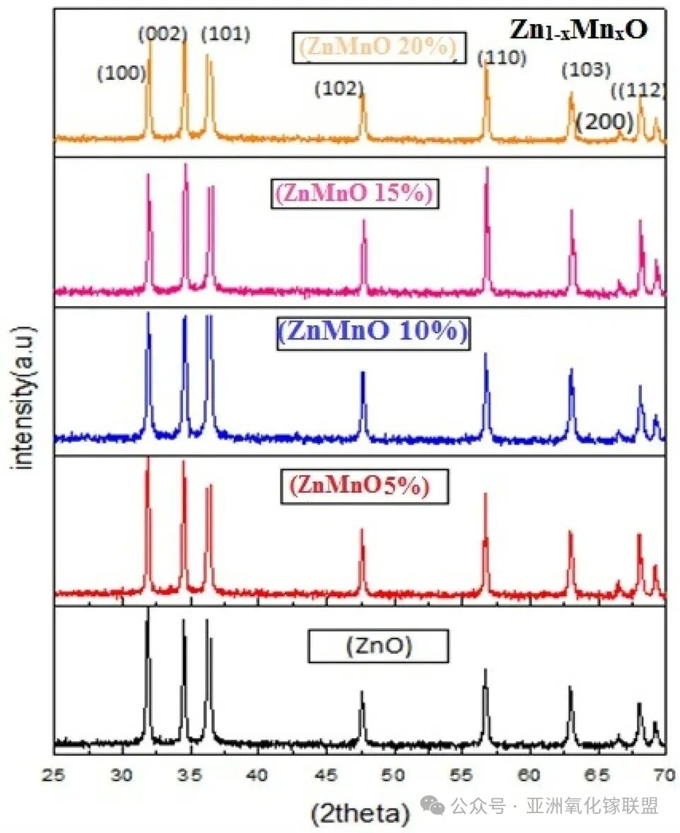
Figure 1. XRD patterns of Zn₁₋ₓMnₓO with different Mn concentrations. The main wurtzite diffraction peaks gradually shift with increasing Mn incorporation, while no secondary phase peaks are observed. DOI: 10.1038/s41598-023-35456-2
Taking Mn-doped ZnO as an example, the structural changes induced by doping can be directly observed. ZnO naturally possesses a wurtzite crystal structure. When the Mn doping concentration increases from 0 to 20%, the XRD diffraction peaks exhibit a systematic shift, while no additional diffraction peaks corresponding to secondary phases are detected. This indicates that Mn atoms are mainly incorporated into the ZnO lattice through substitutional doping, forming a continuous solid solution rather than precipitating as an independent secondary phase.
The shift in diffraction peak positions indicates changes in interplanar spacing, demonstrating that the lattice parameters have been modified by doping. The direction of peak movement can further reveal whether the lattice undergoes expansion or contraction, providing insight into the atomic size mismatch between dopant ions and host ions. Therefore, structural modification represents the foundation of doping effects.
Only when foreign atoms are genuinely incorporated into the host lattice and occupy specific lattice sites can they further regulate the electronic structure, valence states, and carrier distribution of the material. If dopant elements merely remain on the surface or precipitate as secondary phases, they are unlikely to produce substantial modifications to the intrinsic electronic properties of the host material.
How Does Doping Alter Lattice Geometry and Local Structure?
Doping initially affects the crystal structure of a material, and these structural changes can generally be understood at two different levels. The first is the lattice parameters, which reflect the overall averaged structural characteristics of the crystal; the second is the local bond lengths and coordination environments around dopant atoms. These two aspects describe different structural features: lattice parameters reveal the average structural response of the entire crystal, while local structural analysis provides insight into atomic-scale distortions occurring around dopant sites. Only by combining information from both scales can the structural evolution induced by doping be fully understood.
Lattice Constants and Unit Cell Volume
When dopant atoms enter a crystal lattice through substitution and their ionic radii differ from those of the host atoms, the average lattice constants generally vary continuously with increasing dopant concentration. If the substituting ions have larger ionic radii, the lattice tends to expand, leading to increased lattice constants. Conversely, if the dopant ions are smaller, lattice contraction may occur. Such monotonic changes with doping concentration are also important evidence for determining whether the dopant forms a solid solution within the host lattice.
Taking Mn-doped ZnO as an example, the ionic radius of Mn²⁺ is slightly larger than that of Zn²⁺. Therefore, when Mn²⁺ substitutes for Zn²⁺ sites, it induces lattice expansion in ZnO. Experimentally, the lattice constants generally exhibit a continuous variation with increasing Mn concentration, consistent with the empirical Vegard’s law. Significant deviations from this trend often indicate that the dopant concentration is approaching or exceeding the solubility limit, or that phenomena such as elemental segregation and phase separation have occurred within the material.
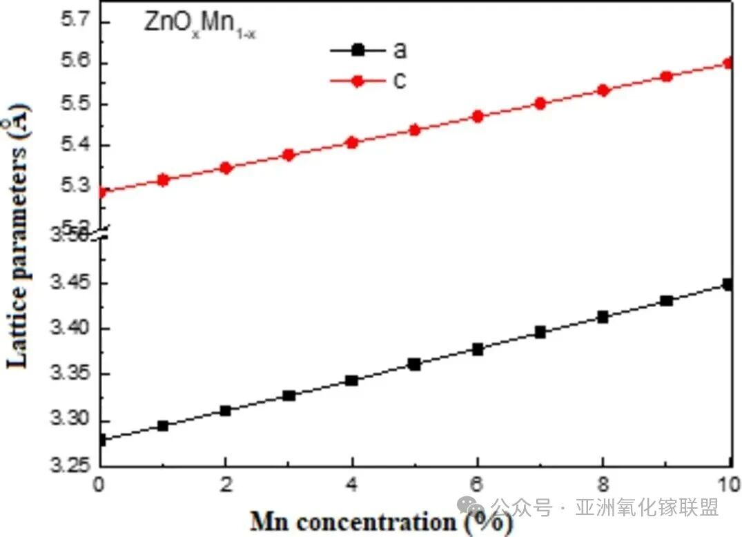
Figure 2. Variation of lattice constants a and c in Zn₁₋ₓMnₓO with increasing Mn concentration. Both lattice parameters exhibit an approximately linear increase with increasing Mn content. DOI: 10.1038/s41598-025-90425-1
The variation of lattice constants with doping concentration can be quantitatively plotted. When the Mn content increases from 0 to 10%, both the a-axis and c-axis lattice constants exhibit an approximately linear increase, corresponding to an expansion of the unit cell volume. This near-linear relationship indicates that Mn atoms are stably incorporated into substitutional sites within this concentration range and that the doping level can be effectively controlled. It also suggests that the extent of lattice expansion can be used to estimate the actual amount of Mn incorporated into the crystal lattice.
The lattice constants measured at the macroscopic scale represent the average structural response of the entire crystal.
Local Bond Length and Coordination Environment
In addition to average lattice parameters, doping can also modify the local structure surrounding dopant atoms, including the bond lengths between dopants and their nearest-neighbor atoms, coordination numbers, and the geometry of coordination polyhedra. These local structural changes do not necessarily follow the same trend as the average lattice parameters, because dopant atoms exert localized interactions on surrounding atoms, causing them to move closer or farther away. As a result, local lattice distortions can form around the dopant sites, but these distortions may not be detectable in the overall averaged crystal structure.
Local structural information is commonly characterized using X-ray absorption spectroscopy techniques, including X-ray absorption near-edge structure (XANES) and extended X-ray absorption fine structure (EXAFS). These techniques are highly sensitive to the atomic environment within several angstroms around dopant atoms. Even when XRD diffraction peaks of the host material show little or no noticeable change, XANES/EXAFS can still reveal variations in bond lengths, coordination numbers, and local coordination configurations around the dopant sites.
Therefore, XANES/EXAFS and XRD provide complementary structural information, together enabling a more comprehensive understanding of the structural evolution induced by doping.
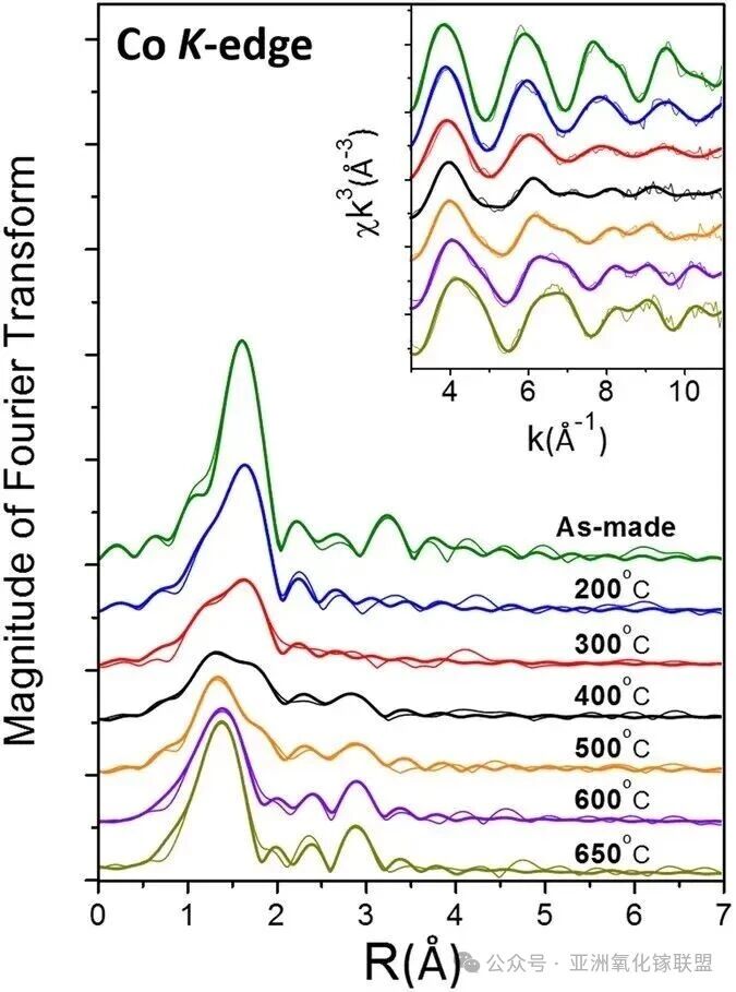
Figure 3. Fourier-transformed Co K-edge EXAFS spectra of Co-doped CeO₂ at different annealing temperatures (inset: k-space EXAFS signals). The nearest-neighbor coordination shells evolve with increasing annealing temperature. DOI: 10.1038/s41598-017-05046-0
The EXAFS results of Co-doped CeO₂ demonstrate how doping can modify the local atomic structure. In the Fourier-transformed EXAFS spectra, the first main peak corresponds to the coordination shell between Co atoms and their nearest-neighbor oxygen atoms. With increasing annealing temperature, changes in the peak position and intensity indicate variations in the Co–O bond length and coordination number.
These local structural changes can occur even when the average lattice structure remains nearly unchanged. Therefore, to fully understand what is altered by doping, it is necessary to consider both the average crystal structure revealed by XRD and the local atomic environment around dopant atoms revealed by EXAFS. Only by combining information from both techniques can the structural effects of doping be comprehensively understood.
The distortion of local bond lengths and coordination environments can further modify the orbital energy levels of dopant atoms, providing the foundation for subsequent changes in the electronic structure.
How Does Doping Alter Electronic Structure?
After the crystal structure is modified by doping, the electronic structure of the material is subsequently redistributed. Dopant atoms possess electronic orbitals and charge characteristics that differ from those of the host atoms. When incorporated into the lattice, they can introduce new electronic states and modify the original band structure and density of states, thereby altering the electronic properties of the material.
Band Structure and Bandgap
Doping can modify the bandgap by introducing new electronic energy levels or shifting the positions of the band edges. Because the energy levels of valence electron orbitals in dopant atoms differ from those of the host atoms, their incorporation into the lattice may generate impurity states within the bandgap or interact with the host bands through orbital hybridization, leading to shifts in the conduction band minimum or valence band maximum.
The direction and magnitude of bandgap variation mainly depend on the relative energy positions between the dopant orbitals and the host band structure. When dopant-derived energy levels are located within the bandgap, they can form intermediate states that participate in electronic excitation processes. In contrast, when these energy levels are close to the conduction band or valence band edges, they are more likely to modify the band-edge positions through orbital hybridization, thereby regulating the bandgap width.
Overall, doping does not simply add extra atoms into a material; it reconstructs the electronic landscape of the host crystal by introducing new states and modifying orbital interactions. These electronic structure changes ultimately determine how doping influences carrier transport, optical absorption, and other functional properties.
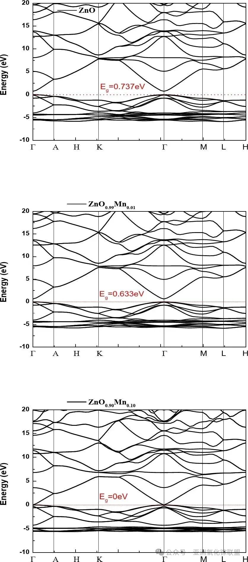
Figure 4. Band structures of ZnO, ZnO₀.₉₉Mn₀.₀₁, and ZnO₀.₉₀Mn₀.₁₀. The bandgap (Eg decreases from 0.737 eV to 0.633 eV and eventually to 0 eV with increasing Mn concentration. DOI: 10.1038/s41598-025-90425-1
Taking Mn-doped ZnO as an example, electronic structure calculations can intuitively demonstrate the effect of doping on material properties. As the Mn doping concentration increases from pristine ZnO to 1% and further to 10%, the band gap (Eg) gradually decreases from 0.737 eV to 0.633 eV, and eventually closes to 0 eV at 10% doping. The underlying mechanism lies in the introduction of new electronic states within the band gap by the Mn 3d orbitals, which interact with the original ZnO electronic bands through orbital hybridization, causing the conduction band minimum and valence band maximum to gradually approach each other.
A reduced band gap means that less energy is required for electrons to transition from the valence band to the conduction band, thereby altering the electrical conductivity and optical absorption characteristics of the material. This mechanism is also one of the key reasons why doping enables many semiconductor materials to extend their optical response range from the ultraviolet region toward the visible-light region.
Density of States and Orbital Contributions
In addition to band structures, the density of states (DOS) describes the distribution of electronic states over different energy ranges. The electronic orbitals of dopant atoms can introduce new electronic states in the DOS spectrum and modify the distribution of states near the Fermi level. Meanwhile, changes in the coordination environment of dopant atoms can alter orbital splitting and energy-level positions, leading to variations in the shape of the DOS curves.
The density of electronic states near the Fermi level plays a critical role in charge transport properties and is one of the key factors determining whether a material exhibits insulating, semiconducting, or metallic behavior.
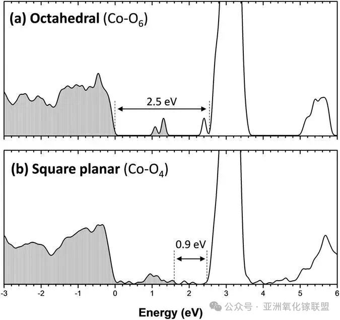
Figure 5. Density of states of Co-doped CeO₂ under two different coordination configurations, octahedral Co–O₆ and square-planar Co–O₄, showing band gaps of approximately 2.5 eV and 0.9 eV, respectively. DOI: 10.1038/s41598-017-05046-0
The same dopant element can also exhibit different electronic structures under different local coordination environments. Taking Co doping as an example, when Co atoms are located in an octahedral Co–O₆ coordination environment, the band gap near the Fermi level is approximately 2.5 eV. However, when the coordination environment changes to square-planar Co–O₄, the band gap decreases to approximately 0.9 eV.
This phenomenon demonstrates that the local coordination environment of dopant atoms can regulate the orbital splitting behavior, redistribute electronic states near the Fermi level, and modify the band gap width. Therefore, a direct connection exists between local structure and electronic structure: the local coordination environment serves as the fundamental origin of electronic structure modification, while changes in the density of states and band gap represent its direct manifestations.
Even when the dopant element remains unchanged, variations in coordination configuration alone can lead to significant differences in the electronic state distribution near the Fermi level and the band gap width, ultimately affecting the electrical conductivity and surface adsorption properties of the material.
How Does Doping Modify Valence States and Carrier Concentration?
In addition to structural and electronic state changes, doping further regulates the internal charge distribution of materials, mainly through changes in the valence states of host elements and variations in free carrier concentration. The former reflects the redistribution of electrons among different atoms, while the latter determines the number of electrons or holes available for electrical transport. Both processes fundamentally originate from the difference in valence states between the dopant and host elements.
Valence States and Charge Compensation
When the valence state of a dopant differs from that of the substituted host atom, heterovalent doping occurs. To maintain overall charge neutrality, the crystal must compensate for the charge imbalance through various mechanisms. These compensation processes typically involve changes in the valence states of neighboring host atoms or the formation of point defects such as vacancies.
For example, when a lower-valence cation replaces a higher-valence host cation, the system may compensate for the charge difference by increasing the valence state of adjacent host cations or by generating anion vacancies.
Doping-induced valence changes can be analyzed using X-ray photoelectron spectroscopy (XPS). Different valence states exhibit distinct binding energies, leading to peak shifts or the appearance of separable spectral components, allowing the valence states of elements and their evolution processes to be identified.
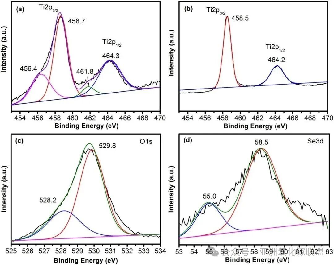
Figure 6. XPS spectra of Se-doped TiO₂: (a) Ti 2p spectrum showing the emergence of a Ti³⁺ component in addition to the Ti⁴⁺ main peak; (b) Ti 2p spectrum after annealing, dominated by Ti⁴⁺; (c) O 1s spectrum; (d) Se 3d spectrum. DOI: 10.1038/s41598-018-27135-4
The Ti 2p XPS spectra of Se-doped TiO₂ reveal doping-induced valence state changes. In the insufficiently oxidized sample, besides the main Ti⁴⁺ peak, an additional Ti³⁺ component appears at lower binding energy, indicating partial reduction of Ti caused by doping and oxygen vacancies. After annealing, the Ti³⁺ component decreases, and Ti⁴⁺ becomes the dominant valence state again. The emergence of mixed valence states in host cations represents a typical signature of doping-induced charge compensation and demonstrates how doping can modify the internal charge distribution of materials.
Carrier Concentration and Type
Heterovalent doping not only modifies the internal charge distribution of materials but also directly affects carrier generation. When higher-valence elements substitute for lower-valence host atoms, they can act as donors by providing additional electrons to the system, causing the material to exhibit n-type conductivity. Conversely, when lower-valence elements replace higher-valence host atoms, they can introduce holes as acceptors, resulting in p-type characteristics.
The concentration and type of carriers directly determine the electrical conductivity of a material. These parameters can typically be obtained through Hall effect measurements, which provide information on carrier concentration and conductivity type. Therefore, doping serves as a key approach for controlling the electrical conductivity type and carrier concentration of semiconductors.
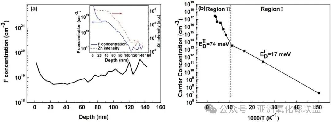
Figure 7. F-doped Mg₀.₅₁Zn₀.₄₉O: (a) depth profile of F concentration; (b) temperature-dependent Hall measurement showing carrier concentration variation as a function of 1000/T, revealing two donor levels. DOI: 10.1038/srep15516
Taking the MgZnO doping system as an example, the introduction of F as a donor significantly increases the carrier concentration compared with the undoped sample, while simultaneously reducing the electrical resistivity. Further temperature-dependent Hall measurements reveal two donor levels at approximately 17 meV and 74 meV, indicating that doping not only modifies the crystal structure and electronic band structure but also directly regulates the number and type of free charge carriers participating in electrical transport.
Through this mechanism, doping establishes a direct link between microscopic electronic structure modulation and macroscopic electrical property changes.
How Do These Changes Manifest in Band Structure and Optical Properties?
The structural changes, electronic structure modifications, and variations in valence states and carrier concentrations discussed above ultimately translate into measurable macroscopic properties of materials. Among them, band gap regulation directly affects light absorption and emission behavior, making optical characterization an important approach for analyzing doping effects. Since the absorption edge is closely related to the band gap and can be measured relatively conveniently, optical absorption spectroscopy is widely used to quickly evaluate whether doping has induced changes in electronic structure.
When doping reduces the band gap, the optical absorption edge shifts toward longer wavelengths, corresponding to lower photon energies. By combining absorption spectroscopy with Tauc analysis, the optical band gap of different doped samples can be obtained through linear extrapolation. The variation of optical band gap with doping concentration not only provides experimental verification of the band structure evolution predicted by theoretical calculations but also serves as evidence that dopants have successfully incorporated into the lattice and achieved the expected electronic structure modulation.
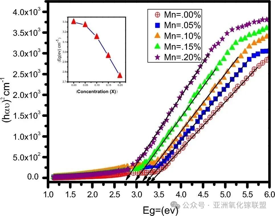
Figure 8. Tauc plots of ZnO with different Mn concentrations ((αhν)²–energy curves), with the inset showing the variation of optical band gap (Eg) with Mn content. DOI: 10.1038/s41598-023-35456-2
Using Mn-doped ZnO as an example, the Tauc plot clearly demonstrates the bandgap variation induced by doping. As the Mn content increases from 0 to 20%, the optical bandgap obtained by linear extrapolation continuously decreases from approximately 3.3 eV to about 2.75 eV. This trend is consistent with the bandgap narrowing predicted by theoretical calculations. The observed optical response represents the final manifestation of a series of changes, including lattice distortion, local coordination adjustment, reconstruction of the electronic structure and density of states, as well as valence-state and carrier regulation.
Overall, the influence of doping on material properties follows a continuous pathway from microscopic structure to macroscopic performance. The difference in atomic size and charge between dopant atoms and host atoms first induces changes in lattice parameters and local bonding structures. These local structural modifications subsequently regulate the electronic structure and density of states through changes in coordination environments. In the case of aliovalent doping, charge compensation further alters the valence states of elements and tunes carrier concentrations, ultimately leading to changes in macroscopic properties such as bandgap, electrical conductivity, and light absorption. Therefore, understanding the mechanism of doping essentially requires tracing the structure–electronic–property relationship and systematically analyzing what is modified at each level within the material.
Instruction
Official Account

Cooperation
Top
