


Recently, Professor Zhaofu Zhang's research team at Wuhan University published a paper in Nano Letters entitled "Achieving Fermi-Level Depinning and Ideal Metal Contacts in β-Ga₂O₃ Devices via MXene Integration." Doctoral student Jiaren Feng from Wuhan University is the first author of the paper, while Professor Zhaofu Zhang, a member of Academician Sheng Liu's research team at the School of Integrated Circuits, Wuhan University, serves as the corresponding author.
Background
The quality of metal–semiconductor contacts is a key factor determining semiconductor device performance. Due to the presence of semiconductor surface states and metal-induced gap states (MIGS), the Fermi level is typically pinned at a specific energy within the semiconductor bandgap, a phenomenon known as Fermi-level pinning, which fundamentally limits the design flexibility of semiconductor devices.
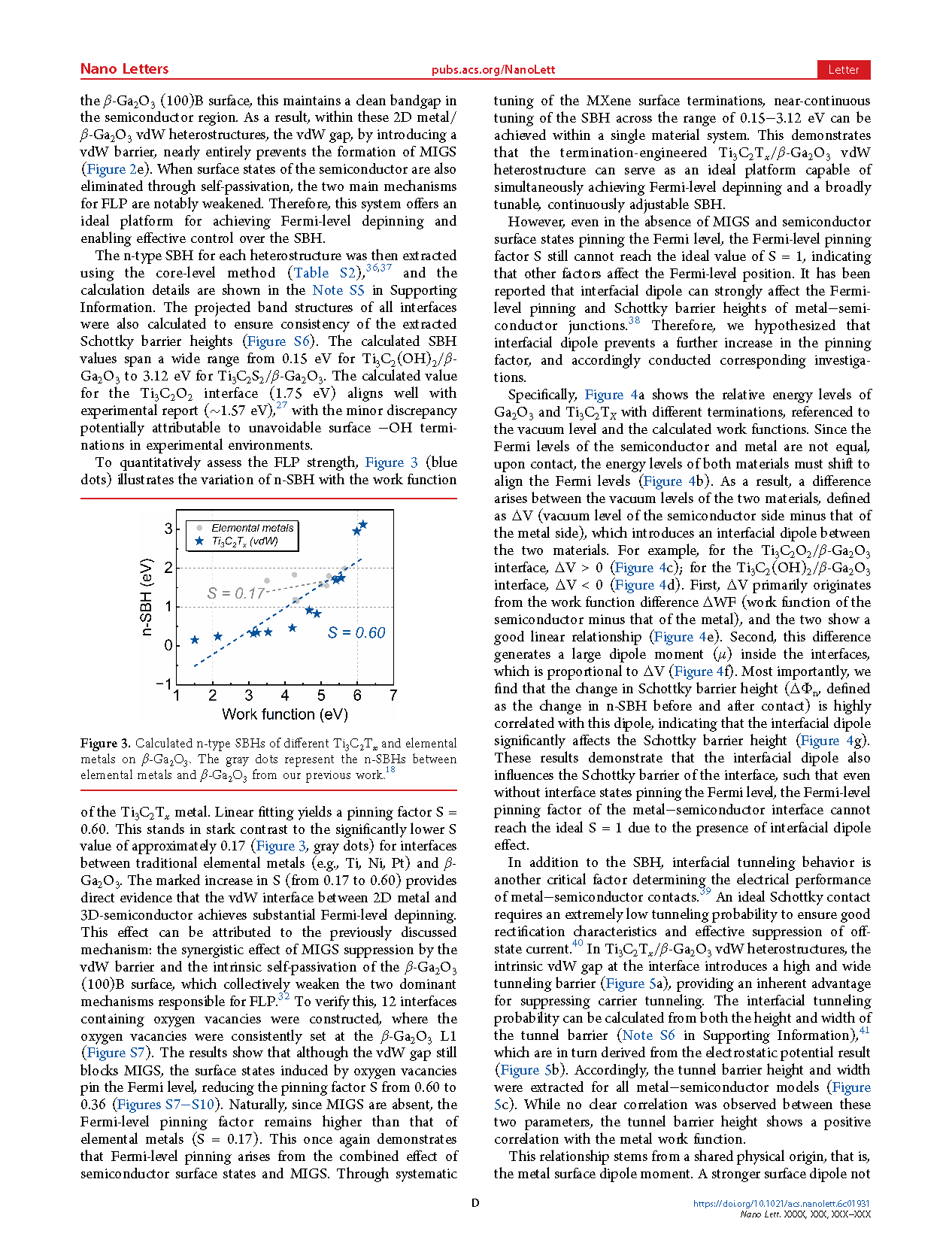
With its ultra-wide bandgap and high critical breakdown electric field, β-Ga₂O₃ has emerged as a highly promising material for next-generation high-power electronic devices. However, its development is significantly hindered by severe Fermi-level pinning at the metal contact interface. The reported Fermi pinning factor of S ≈ 0.17 indicates strong pinning, posing a major challenge to the electrical modulation of the Schottky barrier and highlighting the urgent need for effective depinning strategies.
Previous studies have shown that the van der Waals gap between two-dimensional (2D) metals and 2D semiconductors can suppress the propagation of electron wavefunctions from the metal into the semiconductor. Inspired by this concept, we propose integrating 2D metals with β-Ga₂O₃ to reduce the wavefunction overlap at the metal–semiconductor interface, thereby achieving Fermi-level depinning. However, the underlying physical mechanisms governing such 2D metal/3D semiconductor interfaces remain insufficiently understood from a theoretical perspective.
In addition, an important practical question remains: Can both tunable Schottky contacts and ultra-low-resistance Ohmic contacts be realized within the same material system through different interface engineering strategies?
Abstract
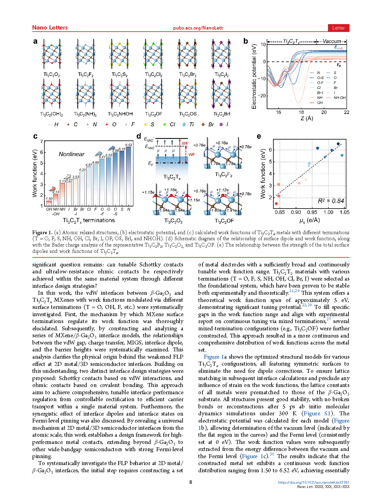
This work systematically investigates the van der Waals interfaces between β-Ga₂O₃ and Ti₃C₂Tₓ MXenes with different surface terminations (T = O, OH, F, etc.). First, a Ti₃C₂Tₓ MXene metal library with tunable work functions ranging from 1.50 to 6.52 eV was established. It was found that different surface terminations primarily regulate the work function by modifying the surface dipole moment of MXenes.
Subsequently, a series of MXene/β-Ga₂O₃ interface models were constructed and analyzed to systematically explore the relationships among van der Waals gaps, charge transfer, interface states, interfacial dipoles, and barrier heights. The results reveal that the interfacial van der Waals barrier effectively suppresses metal-induced gap states (MIGS), thereby enabling Fermi-level depinning. The Schottky barrier height can be continuously tuned within a wide range of 0.15–3.12 eV, with a pinning factor as high as S ≈ 0.60, significantly exceeding that of conventional three-dimensional elemental metal/β-Ga₂O₃ contacts (S ≈ 0.17).
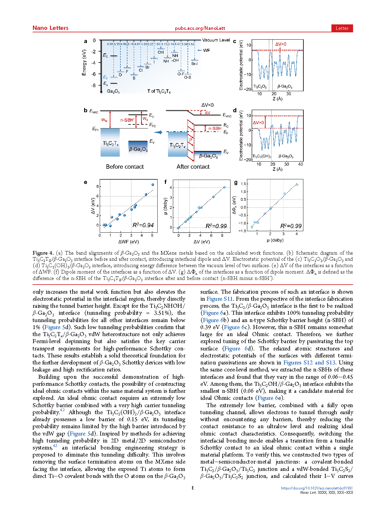
Meanwhile, the study demonstrates that interfacial dipoles also play a significant role in modulating Schottky barrier heights. As a result, even in the absence of metal-induced gap states and semiconductor surface states, the Fermi-level pinning factor cannot reach the ideal value of S = 1.
Based on these findings, two distinct interface engineering strategies are proposed: van der Waals interaction-based Schottky contacts and covalent bonding-based Ohmic contacts. These approaches enable the realization of both widely tunable Schottky barriers and ideal Ohmic contacts within the same material system, providing a new pathway for designing high-performance β-Ga₂O₃ electronic devices.
Conclusion
In this work, the interfacial electronic structure and contact properties of Ti₃C₂Tₓ MXene/β-Ga₂O₃ heterostructures (T = O, OH, F, etc.) were systematically investigated, providing a new strategy for addressing the severe Fermi-level pinning issue in wide-bandgap semiconductors.
First, the physical origin of the continuously tunable work function of MXenes (1.50–6.52 eV) was clarified, demonstrating that surface termination atoms precisely regulate the work function by modifying the surface dipole. Subsequently, in the constructed β-Ga₂O₃/Ti₃C₂Tₓ van der Waals heterostructures, the interfacial van der Waals barrier was found to effectively suppress metal-induced gap states (MIGS). Combined with the self-passivating nature of the β-Ga₂O₃ surface, the Fermi-level pinning factor was significantly enhanced to S ≈ 0.60, substantially outperforming conventional three-dimensional elemental metal contacts (S ≈ 0.17).
Within this single material platform, the Schottky barrier height (SBH) can be continuously tuned over a wide range of 0.15–3.12 eV, while the tunneling probability remains below 5%, satisfying the requirements for high-performance Schottky contacts. Moreover, the study reveals that, due to the presence of an interfacial dipole, the Fermi-level pinning factor cannot reach the ideal value of S = 1, even in the absence of interface states.
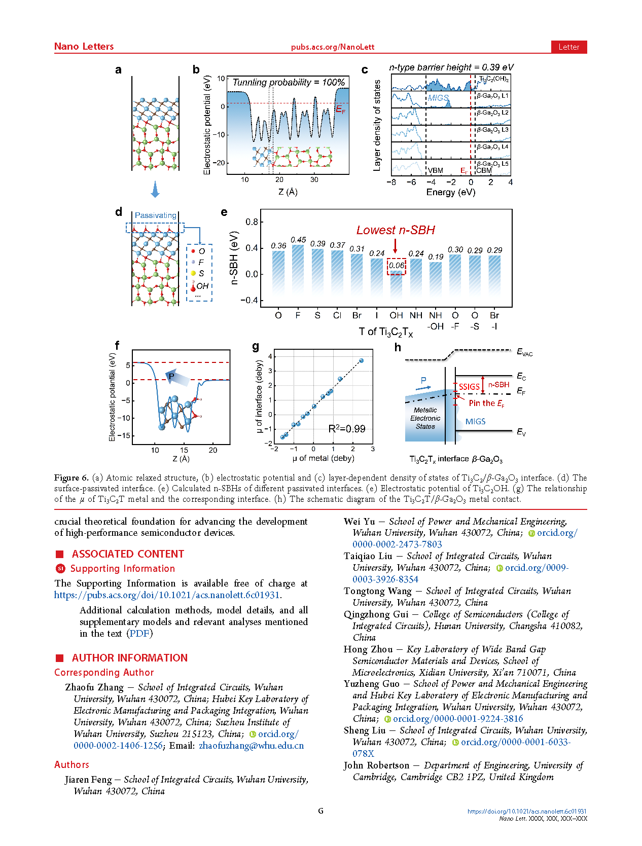
Furthermore, by transforming the interfacial interaction from van der Waals coupling to Ti–O covalent bonding, an ideal Ohmic contact can be achieved, exhibiting a 100% tunneling probability and an ultra-low barrier height of only 0.06 eV. This covalent bonding configuration pins the Fermi level near the conduction band minimum of β-Ga₂O₃, thereby producing ideal Ohmic contact characteristics. Notably, this behavior is largely insensitive to both the surface termination groups and the intrinsic polarity of the MXene.
This work demonstrates the capability to engineer both tunable Schottky contacts and high-performance Ohmic contacts within the same 2D metal/3D semiconductor system through interface design. It provides a new approach to overcoming the long-standing challenge of Fermi-level pinning and establishes a solid theoretical foundation for the development of next-generation high-performance semiconductor devices.
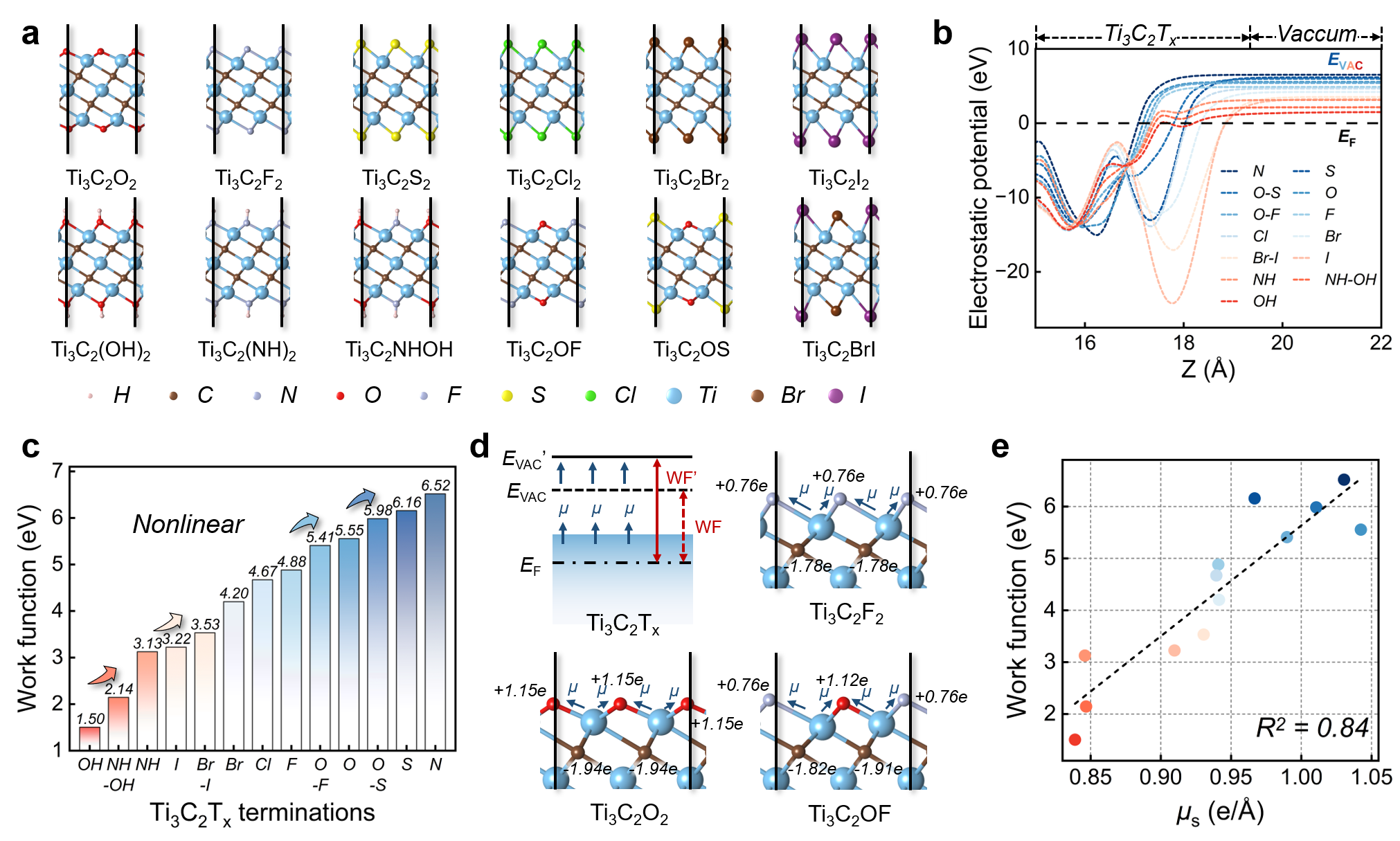
FIG 1. (a) Relaxed atomic structures, (b) electrostatic potential profiles, and (c) calculated work functions of Ti₃C₂Tₓ MXenes with different surface terminations (T = O, F, S, NH, OH, Cl, Br, I, OF, OS, BrI, and NHOH). (d) Schematic illustration of the relationship between surface dipoles and work function, together with Bader charge analysis of representative Ti₃C₂F₂, Ti₃C₂O₂, and Ti₃C₂OF. (e) Correlation between the total surface dipole strength and the work function of Ti₃C₂Tₓ MXenes.
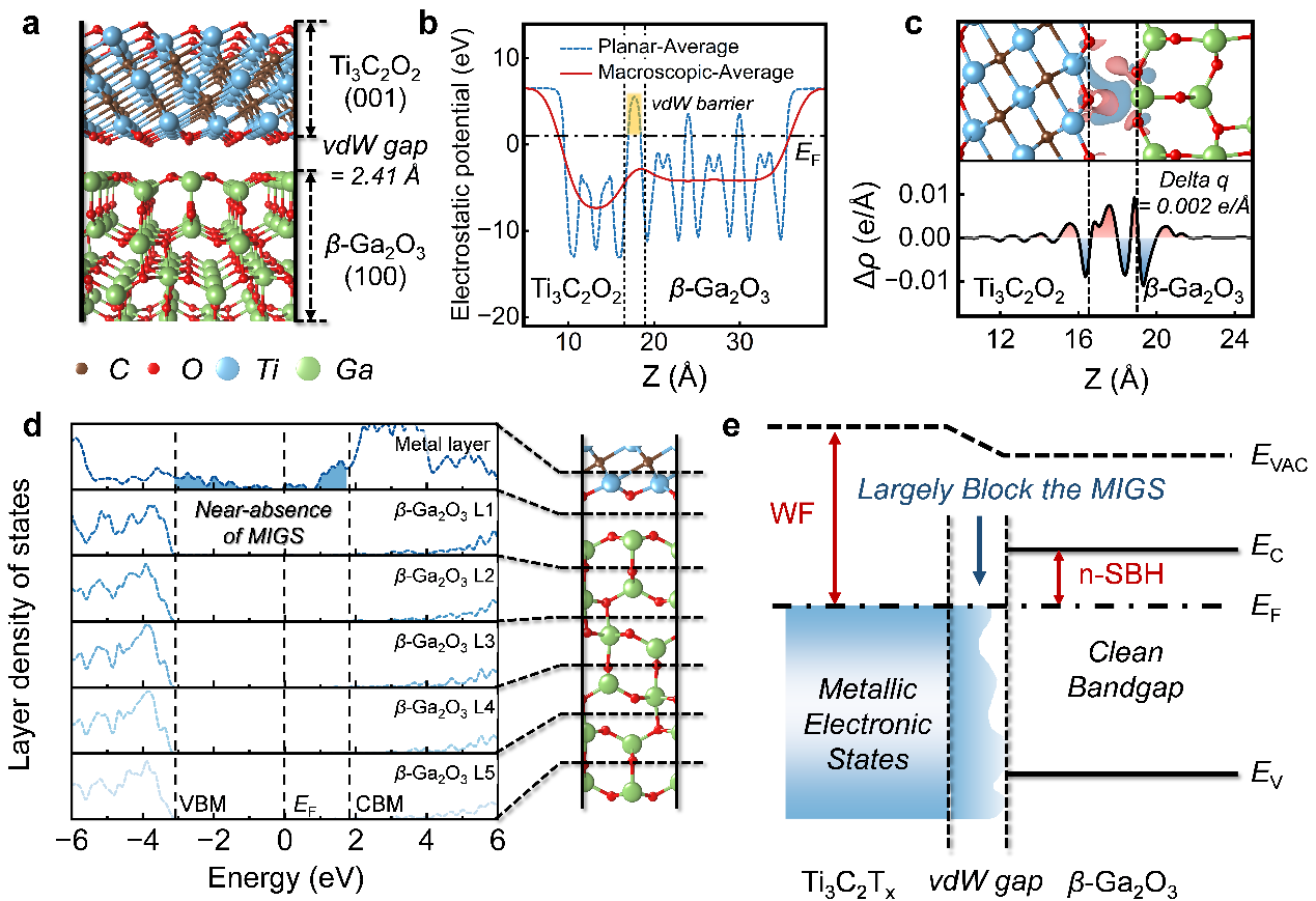
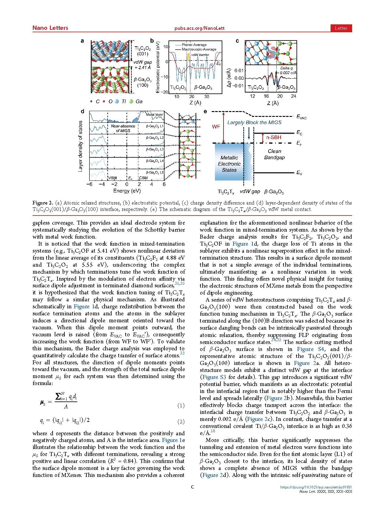
FIG 2. (a) Relaxed atomic structure, (b) electrostatic potential, (c) charge density difference, and (d) layer-resolved density of states (DOS) of the Ti₃C₂O₂(001)/β-Ga₂O₃(100) interface.(e) Schematic illustration of the Ti₃C₂Tₓ/β-Ga₂O₃ van der Waals metal contact.
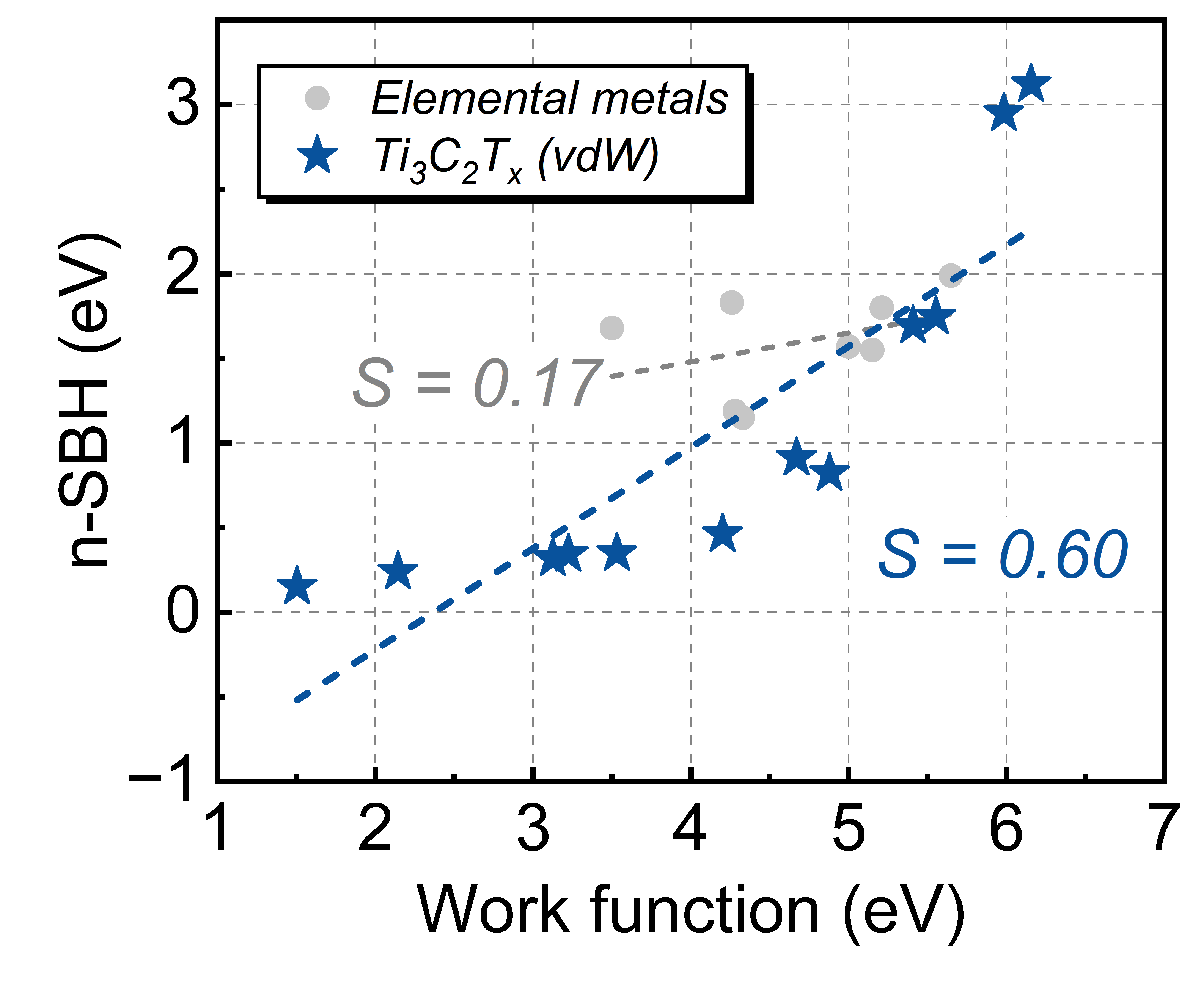
FIG 3. Calculated n-type Schottky barrier heights (SBHs) of different Ti₃C₂Tₓ MXenes and elemental metals on β-Ga₂O₃. The gray dots represent the n-type SBHs between elemental metals and β-Ga₂O₃ reported in our previous work.
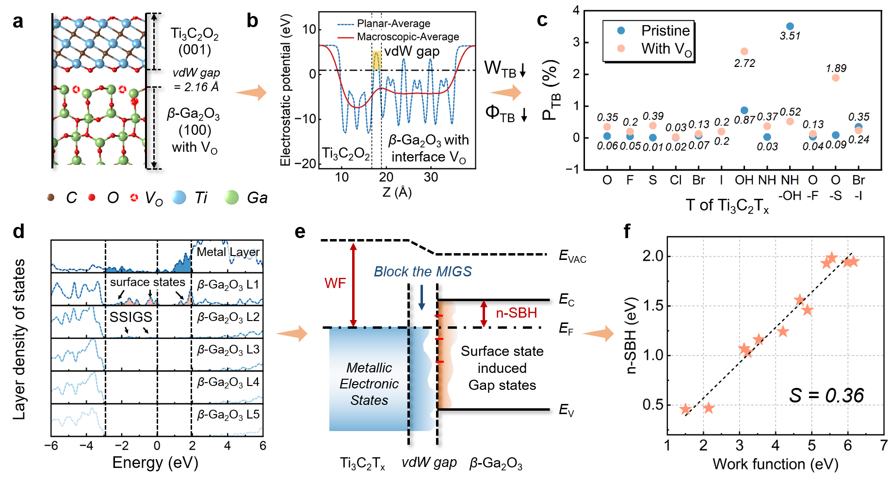
FIG 4. (a) Band alignments of β-Ga₂O₃ and MXene metals based on the calculated work functions. (b) Schematic illustration of the Ti₃C₂Tₓ/β-Ga₂O₃ interface before and after contact, showing the formation of the interfacial dipole and ΔV. (c, d) Electrostatic potential profiles of the Ti₃C₂O₂/β-Ga₂O₃ and Ti₃C₂(OH)₂/β-Ga₂O₃ interfaces, respectively, showing the energy difference between the vacuum levels of the two surfaces. (e) ΔV of the interfaces as a function of ΔWF. (f) Dipole moment of the interfaces as a function of ΔV. (g) ΔΦₙ of the interfaces as a function of dipole moment. Here, ΔΦₙ is defined as the difference between the n-type Schottky barrier height (n-SBH) of the Ti₃C₂Tₓ/β-Ga₂O₃ interface after and before contact (ΔΦₙ = n-SBH − n-SBH′).
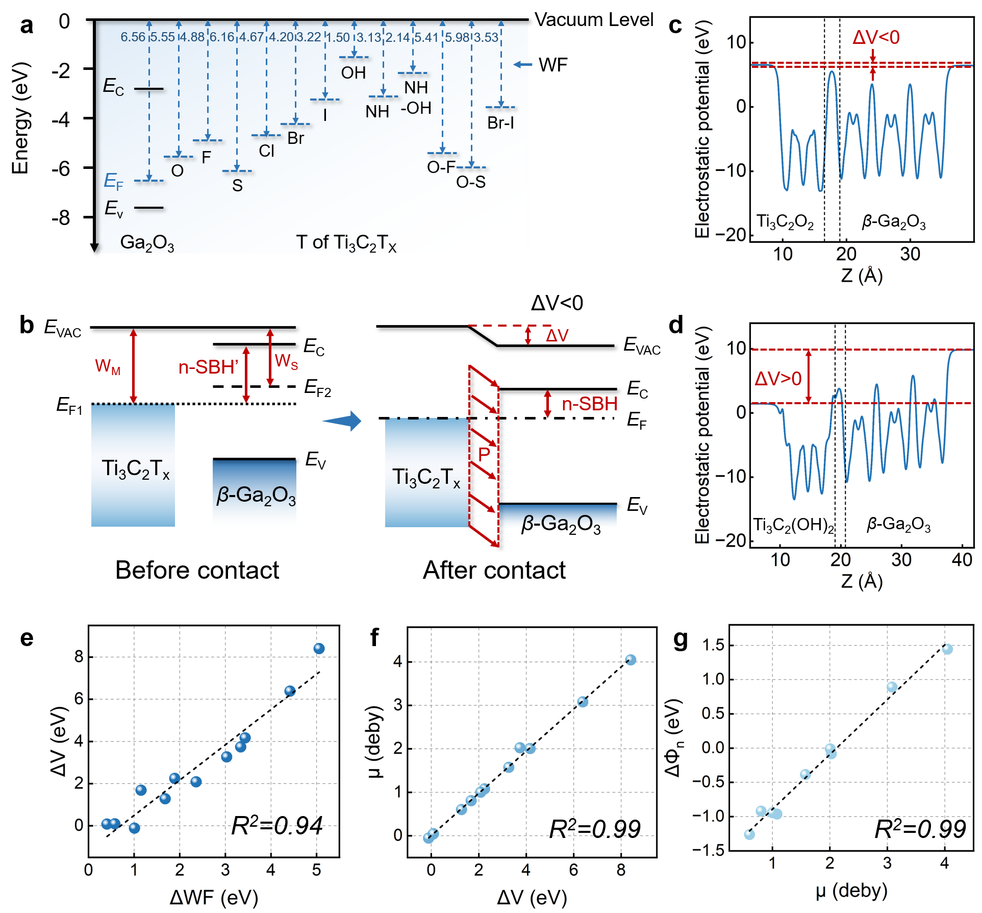
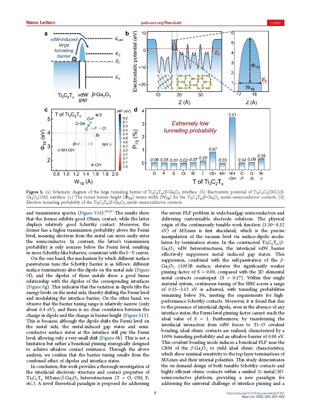
FIG 5. (a) Schematic illustration of the large tunneling barrier at the Ti₃C₂Tₓ/β-Ga₂O₃ interface. (b) Electrostatic potential profile of the Ti₃C₂O₂(001)/β-Ga₂O₃(100) interface. (c) Tunneling barrier height (Φ_TB) and width (W_TB) of Ti₃C₂Tₓ/β-Ga₂O₃ interfaces. (d) Electron tunneling probability of Ti₃C₂Tₓ/β-Ga₂O₃ metal–semiconductor contacts.

FIG 6. (a) Schematic illustration of the large tunneling barrier at the Ti₃C₂Tₓ/β-Ga₂O₃ interface. (b) Electrostatic potential profile of the Ti₃C₂O₂(001)/β-Ga₂O₃(100) interface. (c) Relationship between the tunneling barrier height (Φ_TB) and width (W_TB) of Ti₃C₂Tₓ/β-Ga₂O₃ metal–semiconductor contacts. (d) Calculated electron tunneling probabilities of Ti₃C₂Tₓ/β-Ga₂O₃ metal–semiconductor contacts. All interfaces exhibit small tunneling barriers, satisfying the requirements for high-quality Schottky contacts, but they are unfavorable for achieving ideal Ohmic contacts.
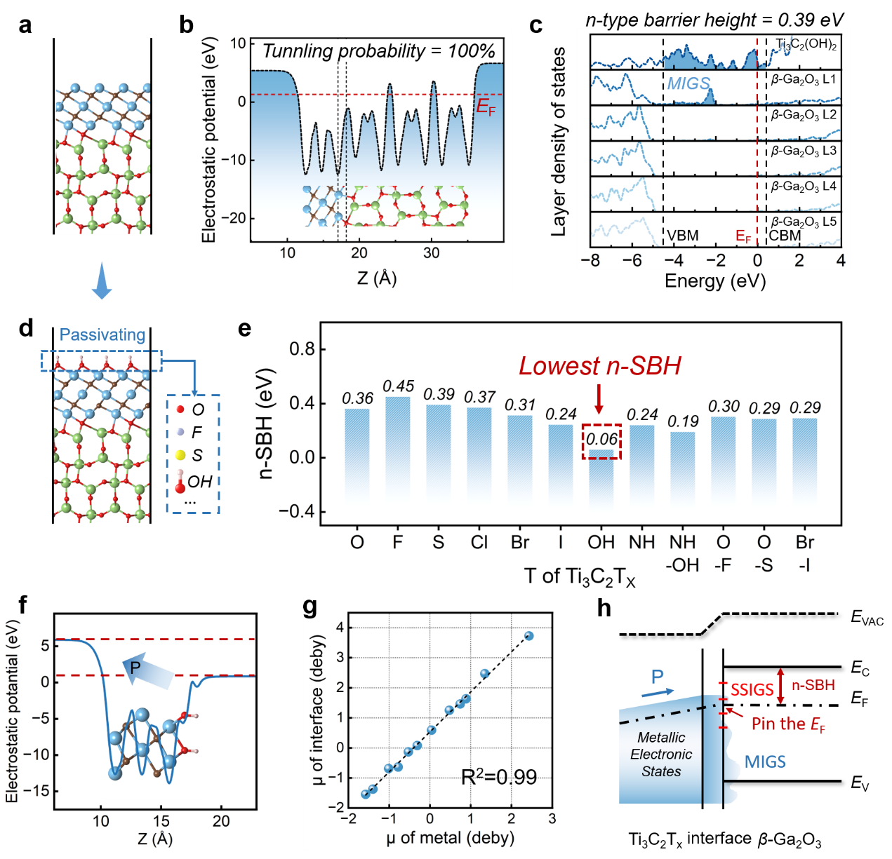
FIG 7. (a) Relaxed atomic structure, (b) electrostatic potential profile, and (c) layer-resolved density of states (DOS) of the covalently bonded Ti₃C₂/β-Ga₂O₃ interface. By converting the interfacial bonding from van der Waals interaction to covalent bonding, the electron tunneling probability reaches 100%, making the interface suitable for ideal Ohmic contacts. (d) Schematic illustration of the surface-passivated interfaces. (e) Calculated n-type Schottky barrier heights (n-SBHs) of different passivated interfaces. Surface passivation further modulates the interfacial barrier, with the Ti₃C₂OH/β-Ga₂O₃ interface exhibiting the lowest n-SBH of 0.06 eV. (f) Electrostatic potential profile of Ti₃C₂OH. (g) Relationship between the dipole moment of Ti₃C₂Tₓ MXenes and that of the corresponding interfaces. (h) Schematic illustration of the Ti₃C₂Tₓ/β-Ga₂O₃ metal contact. Although surface passivation can modify the dipole on the metal side, thereby altering the interfacial dipole and Schottky barrier height, the Fermi level remains pinned by metal-induced gap states (MIGS) and semiconductor surface states at the interface, resulting in only a limited variation in the Schottky barrier height.
DOI:
10.1021/acs.nanolett.6c01931
Instruction
Official Account

Cooperation
Top
