


Researchers from the Zhengzhou University have published a dissertation titled "Superior interfacial thermal conductance between β-Ga2O3 and diamond realized through metal-assisted epitaxial strategy in National Science Review.
Background
As an ultra-wide bandgap semiconductor, β-Ga₂O₃ has outstanding potential for next-generation high-voltage power electronic devices due to its ultrahigh breakdown field. Nevertheless, the intrinsic thermal conductivity of β-Ga₂O₃ only ranges from 10 to 27 W m⁻¹ K⁻¹. Joule heat generated during device operation cannot be dissipated rapidly, which limits the maximum power density and accelerates thermal degradation of devices. The heat dissipation bottleneck has long restricted the industrialization of β-Ga₂O₃ power devices.
Diamond possesses an ultrahigh thermal conductivity of ~2200 W m⁻¹ K⁻¹ and is recognized as the optimal near-junction heat dissipation substrate. Direct epitaxial growth of β-Ga₂O₃ thin films on diamond substrates can rapidly evacuate heat from hot spots close to heat sources, serving as an ideal strategy to solve device thermal management issues. However, β-Ga₂O₃ belongs to monoclinic crystal system while diamond is cubic, leading to extremely large lattice mismatch between the two materials. Traditional fabrication methods such as atomic layer deposition (ALD) and pulsed laser deposition (PLD) tend to generate impurity phases including ε-Ga₂O₃ and γ-Ga₂O₃ at the interface, resulting in poor crystalline quality of thin films. In contrast, low-temperature bonding and van der Waals bonding approaches deliver extremely weak interfacial bonding strength, and interfacial delamination easily occurs under high-temperature operating conditions.
Furthermore, thermal boundary conductance at heterogeneous interfaces directly governs cross-interface heat transfer efficiency. The huge discrepancy in phonon density of states between diamond and β-Ga₂O₃ gives rise to severe phonon scattering loss. Meanwhile, interfacial bonding configuration, surface morphology and thermal expansion mismatch all exert remarkable impacts on interfacial thermal transport. Weak van der Waals interactions drastically hinder phonon transmission, while massive thermal expansion mismatch introduces thermal stress at the gigapascal level and triggers interfacial cracking. Consequently, constructing high-quality β-Ga₂O₃/diamond heterointerfaces with atomically flat surface and covalent bonding is fundamentally essential to realize efficient heat dissipation and guarantee long-term reliability of power devices.
Abstract
β-Ga₂O₃ exhibits great potential for next-generation power electronics, while its low thermal conductivity poses a challenge to efficient heat dissipation. We address this challenge by developing a gallium-assisted epitaxial strategy to synthesize highly oriented β-Ga₂O₃ film on diamond. The β-Ga₂O₃ presents a high thermal conductivity of 9.0 W m⁻¹ K⁻¹ and low thermal boundary resistance of 6.05 m² K GW⁻¹. Experiments reveal a high interfacial bonding strength (>2.09 GPa), resulting from the atomically sharp and covalently bonded interface. The identified new interfacial phonon mode at ∼60 meV through the vibrational electron energy-loss spectroscopy can significantly enhance the phonon transport between diamond and β-Ga₂O₃. The developed gallium-assisted strategy may mitigate the thermal constraints of β-Ga₂O₃ offering a promising route for the heterointegration of β-Ga₂O₃-based power devices with diamond.
Highlights
A novel Ga-assisted CVD epitaxy strategy is proposed to realize atomically flat (2̄01)-oriented β-Ga₂O₃thin films on (111) diamond substrates, free of impurity phases and interfacial interlayers, delivering superior crystalline quality compared with all reported deposition and bonding routes;
C−O covalent bonding is formed at β-Ga₂O₃/diamond heterointerface, achieving ultrahigh interfacial fracture strength over 2.09 GPa, which far outperforms traditional van der Waals bonding and low-temperature direct bonding, greatly improving high-temperature operational reliability of power devices;
A novel localized interfacial phonon mode centered at ~60 meV is directly visualized via vibrational EELS. Combined with molecular dynamics simulations, this phonon mode is verified as the core channel for efficient cross-interface heat transfer, revealing the atomic-scale phonon transport mechanism across heterogeneous interfaces;
The as-grown β-Ga₂O₃thin film achieves a thermal conductivity of 9.0 W m⁻¹ K⁻¹, with thermal boundary conductance of 165.4 MW m⁻² K⁻¹ and ultra-low thermal boundary resistance of 6.05 m² K GW⁻¹, outperforming all previously reported Ga₂O₃/diamond heterostructures in thermal transport performance;
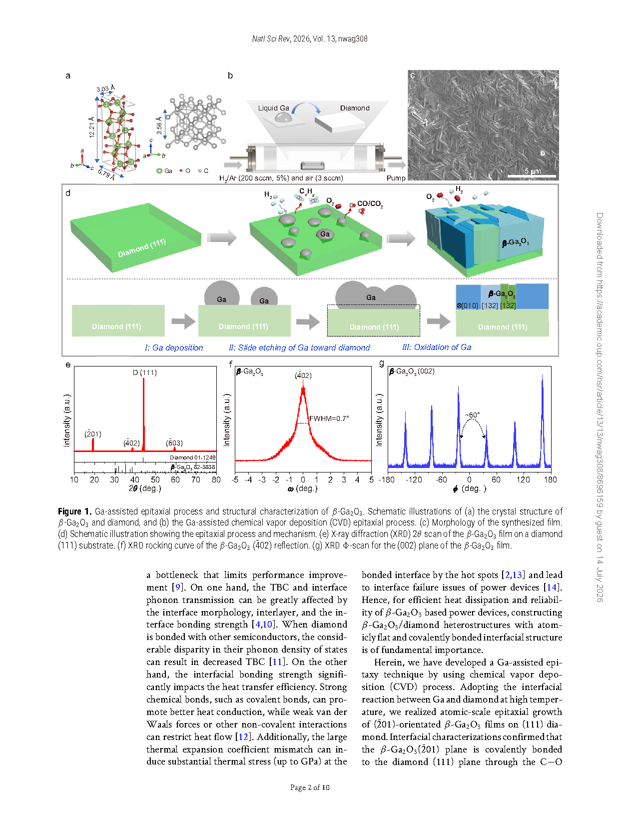
The atomic-scale growth mechanism including liquid Ga catalytic etching of diamond, in-situ elimination of graphite, and oxidation into β-Ga₂O₃ is fully clarified, offering a universal fabrication route for high-quality hetero-integration between ultra-wide bandgap semiconductors and diamond.
Conclusion
In summary, we achieved the atomically epitaxial growth of (2̄01)-oriented β-Ga₂O₃ films on diamond (111) substrate using a CVD method by adopting the interfacial reaction between Ga and diamond. The obtained β-Ga₂O₃ film presents a high κ of 9.0 W m⁻¹ K⁻¹ and a low thermal boundary resistance (TBR) of 6.05 m² K GW⁻¹. The covalent C–O bond at the interface leads to a high interfacial fracture strength over 2.09 GPa. The observed interfacial phonon mode at ∼60 meV provides a phonon transmission channel and significantly improves the TBC. These findings provide insights into the microscopic mechanisms governing phonon transport at the β-Ga₂O₃/diamond interface, and offer a strategy for designing heterogeneous interfaces with both high interfacial bond strength and superior κ thereby paving the way for facilitating advancements in β-Ga₂O₃ based power devices by mitigating the low κ bottleneck issue of β-Ga₂O₃.
Project Support
This work was supported by the National Natural Science Foundation of China (12274371, 52572052, 62271450, 12504007 and 52327808), the International Science and Technology Cooperation in Henan Province (261111521100), the Science and Technology Innovation Leading Talent Support Program of Henan Province (254000510060), the Provincial Science and Technology Major Project of Jiangsu (BG2024030), the Jiangsu Funding Program for Excellent Postdoctoral Talent, and the High-Level Talent Research Start-Up Project Funding of Henan Academy of Sciences (20251827009). Peng Gao acknowledges support from the New Cornerstone Science Foundation through the Xplorer Prize.
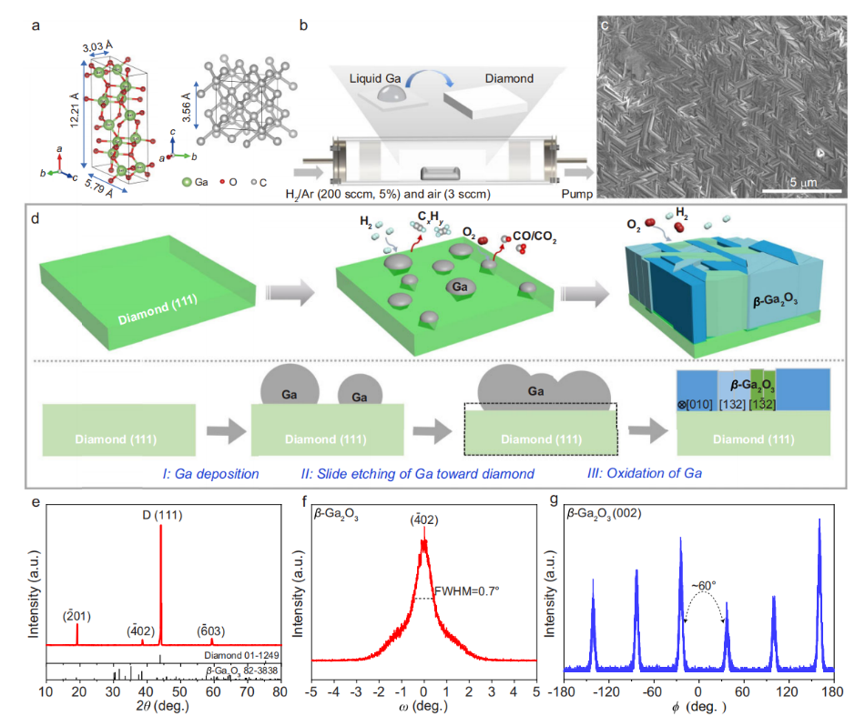
Figure 1. Ga-assisted epitaxial process and structural characterization of β-Ga₂O₃. Schematic illustrations of (a) the crystal structure of β-Ga₂O₃ and diamond, and (b) the Ga-assisted chemical vapor deposition (CVD) epitaxial process. (c) Morphology of the synthesized film. (d) Schematic illustration showing the epitaxial process and mechanism. (e) X-ray diffraction (XRD) 2θ scan of the β-Ga₂O₃ film on a diamond (111) substrate. (f) XRD rocking curve of the β-Ga₂O₃ (402) reflection. (g) XRD φ-scan for the (002) plane of the β-Ga₂O₃ film.
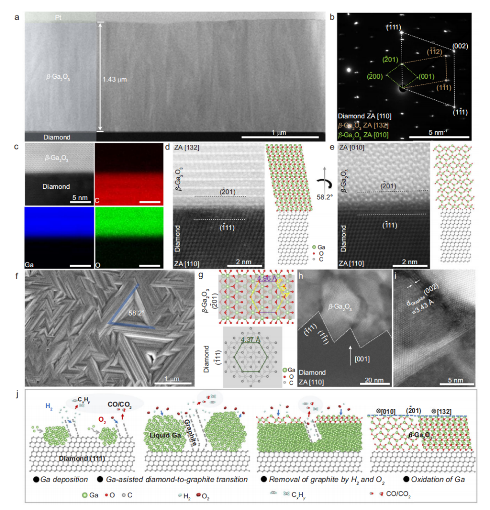
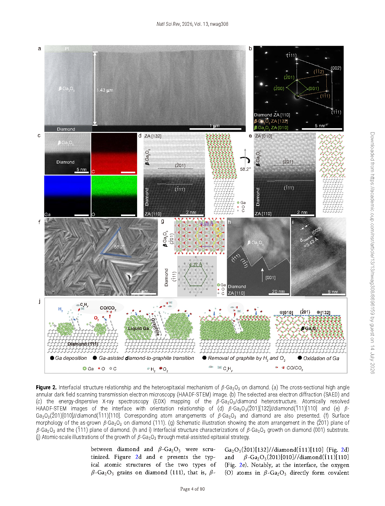
Figure 2. Interfacial structure relationship and the heteroepitaxial mechanism of β-Ga₂O₃ on diamond. (a) The cross-sectional high angle annular dark field scanning transmission electron microscopy (HAADF-STEM) image. (b) The selected area electron diffraction (SAED) and (c) the energy-dispersive X-ray spectroscopy (EDX) mapping of the β-Ga₂O₃/diamond heterostructure. Atomically resolved HAADF-STEM images of the interface with orientation relationship of (d) β-Ga₂O₃(2̄01)[132]//diamond (1̄11)[110] and (e) β-Ga₂O₃(2̄01)[010]//diamond (1̄11)[110]. Corresponding atom arrangements of β-Ga₂O₃ and diamond are also presented. (f) Surface morphology of the as-grown β-Ga₂O₃ on diamond (111). (g) Schematic illustration showing the atom arrangement in the (2̄01) plane of β-Ga₂O₃ and the (1̄11) plane of diamond. (h and i) Interfacial structure characterizations of β-Ga₂O₃ growth on diamond (001) substrate. (j) Atomic-scale illustrations of the growth of β-Ga₂O₃ through metal-assisted epitaxial strategy.
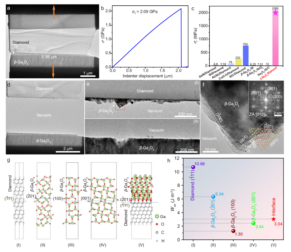
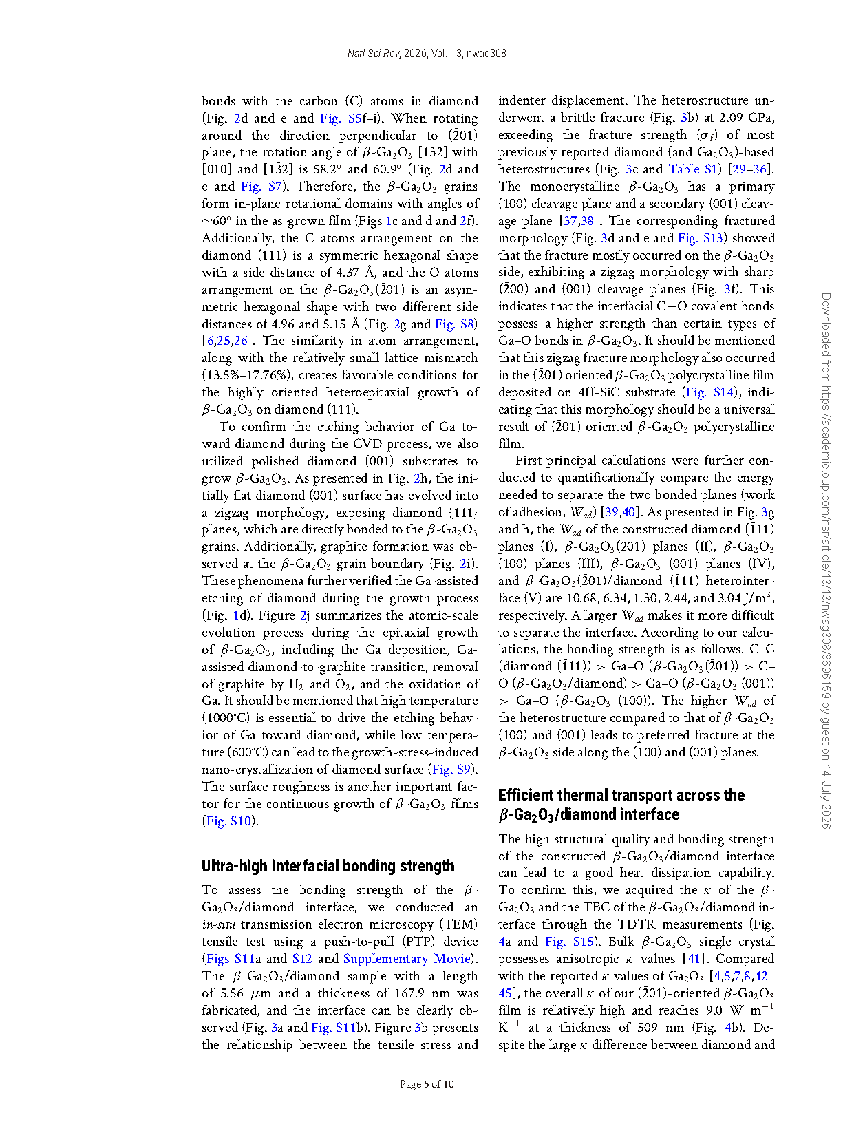
Figure 3. Bonding strength measurement of the β-Ga₂O₃/diamond interface. (a) Transmission electron microscopy (TEM) image of the focused ion beam (FIB)-fabricated β-Ga₂O₃/diamond sample for the tensile test. (b) Relationship between the applied stress and the indenter displacement. (c) The comparison of the fracture strength (σf) of distinct diamond (and Ga₂O₃)-based heterostructures. (d) The low-mag and (e) high-mag TEM images presenting the fracture morphology. (f) High-resolution TEM (HRTEM) image of the remained β-Ga₂O₃ indicated by the frame in (e (I)). Inset shows the corresponding fast Fourier transform (FFT) pattern. (g) Side view models and (h) the corresponding calculated work of adhesion (Wad) for (I) diamond (1̄11), (II) β-Ga₂O₃(2̄01), (III) β-Ga₂O₃(100), (IV) β-Ga₂O₃(001), and (V) β-Ga₂O₃(2̄01)/diamond (1̄11) interface. The dashed line marks the fracture position.
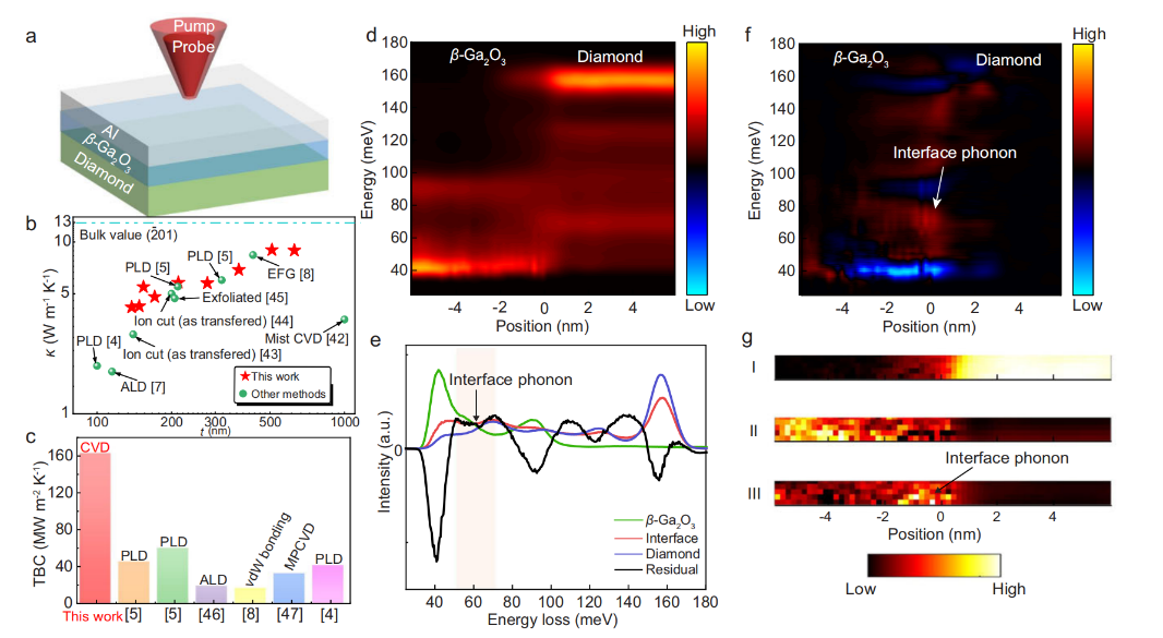
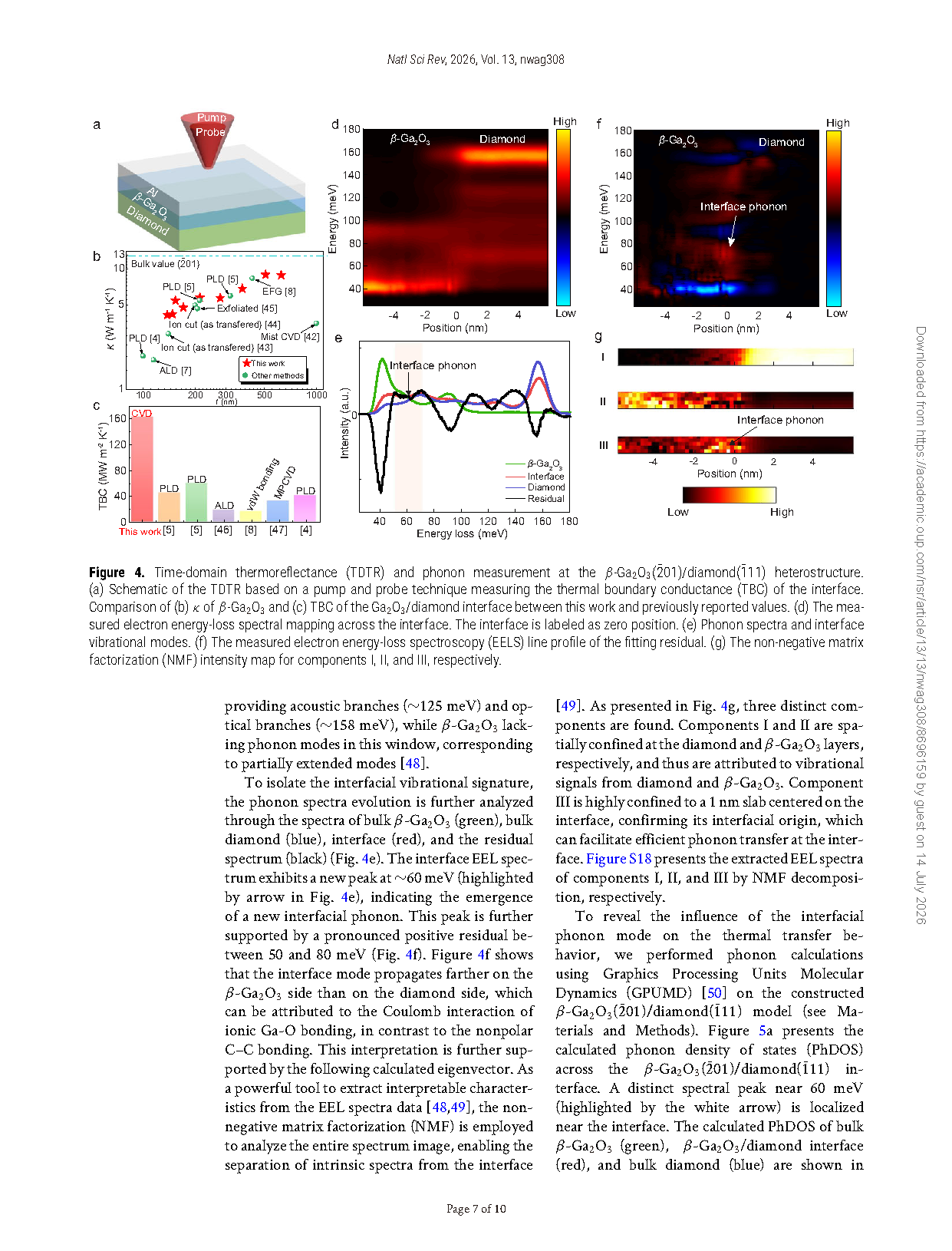
Figure 4. Time-domain thermoreflectance (TDTR) and phonon measurement at the β-Ga₂O₃(2̄01)/diamond (1̄11) heterostructure. (a) Schematic of the TDTR based on a pump and probe technique measuring the thermal boundary conductance (TBC) of the interface. Comparison of (b) κ of β-Ga₂O₃ and (c) TBC of the Ga₂O₃/diamond interface between this work and previously reported values. (d) The measured electron energy-loss spectral mapping across the interface. The interface is labeled as zero position. (e) Phonon spectra and interface vibrational modes. (f) The measured electron energy-loss spectroscopy (EELS) line profile of the fitting residual. (g) The non-negative matrix factorization (NMF) intensity map for components I, II, and III, respectively.
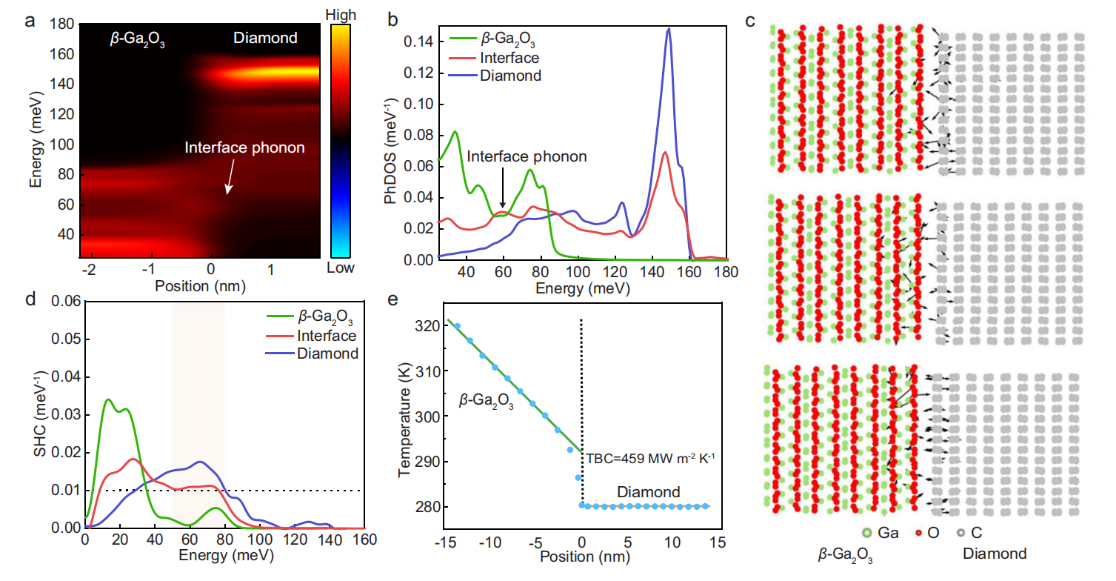
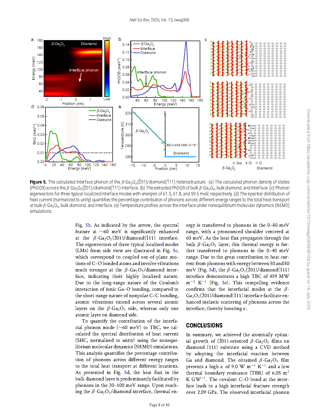
Figure 5. The calculated interface phonon of the β-Ga₂O₃(2̄01)/diamond (1̄11) heterostructure. (a) The calculated phonon density of states (PhDOS) across the β-Ga₂O₃(2̄01)/diamond (1̄11) interface. (b) The extracted PhDOS of bulk β-Ga₂O₃, bulk diamond, and interface. (c) Phonon eigenvectors for three typical localized interface modes with energies of 61.5, 61.8, and 59.5 meV, respectively. (d) The spectral distribution of heat current (normalized to unity) quantifies the percentage contribution of phonons across different energy ranges to the total heat transport at bulk β-Ga₂O₃, bulk diamond, and interface. (e) Temperature profiles across the interface under nonequilibrium molecular dynamics (NEMD) simulations.
DOI :
10.1093/nsr/nwag308
Instruction
Official Account

Cooperation
Top
