


Researchers from Chongqing SanXia University of Science and Technology, Changsha University of Science and Technology & Yan’an University have published a paper titled "Atomic-layer-selective source/drain doping unlocks high current and strong gate control in 1-nm asymmetric monolayer Ga₂O₃ transistors" in Nano Research.
Background
As silicon transistor scaling enters sub-3 nm technology nodes, an inherent trade-off exists between carrier injection and gate electrostatic control. Higher source/drain doping density boosts driving current yet intensifies gate-channel coupling and degrades gate regulation; lighter doping strengthens electrostatic performance at the cost of on-state current. Conventional device architectures cannot resolve this contradiction. Two-dimensional monolayer semiconductors free from dangling-bond surface states act as promising channel candidates for ultra-short-channel devices. Previously reported monolayer GaN, GaSe transistors adopt uniform full doping schemes and fail to break this performance balance. Asymmetric monolayer Ga₂O₃ exhibits intrinsic layer-resolved electronic structures: electrons are confined to bottom Ga-O sublayers while holes occupy top O-Ga-O sublayers, enabling vertical layer modulation. Conventional doping uniformly modulates the whole monolayer without utilizing vertical carrier separation. This work proposes an atomic-layer-selective source/drain doping strategy, which only n-dopes conductive bottom sublayers and keeps upper layers intrinsic to decouple carrier injection and gate electrostatic coupling at atomic scale. First-principles quantum transport simulations combined with non-equilibrium Green’s function are carried out to compare fully doped and locally doped devices. The results verify that this strategy simultaneously delivers high on-current and superior subthreshold characteristics at the ultimate 1 nm gate length, offering a universal design paradigm for ultra-scaled devices based on diverse 2D asymmetric monolayers with vertical carrier separation.
Abstract
As transistor scaling approaches the sub-3 nm regime, two-dimensional (2D) monolayer MOSFETs face a fundamental limitation arising from the intrinsic coupling between carrier injection and gate electrostatic control. Increasing source/drain (S/D) doping improves carrier injection but degrades electrostatics, whereas reduced doping enhances gate control at the expense of driving current. Here, we propose an atomic-layer-selective doping strategy for S/D electrodes in asymmetric monolayer Ga₂O₃ MOSFETs, exploiting the intrinsic layer-resolved electronic structure of monolayer Ga₂O₃, where electrons are predominantly confined to the bottom Ga-O sublayers while holes reside in the top O-Ga-O sublayers. By locally doping (LD) the bottom Ga-O sublayers while keeping the top O-Ga-O sublayers intrinsic, the LD strategy decouples carrier injection from gate control at the atomic-layer scale. Fully doped S/D electrodes are used as a reference benchmark. Quantum transport simulations show that both fully doped and LD devices deliver high driving currents at gate lengths of 3 nm and 2 nm. Notably, layer-confined transport in LD devices substantially enhances electrostatic control, with reduced subthreshold swing and suppressed leakage current, enabling simultaneous high current and robust gate electrostatics at 1 nm. Benefiting from its experimental feasibility, the LD technique establishes a materials-guided, transferable design principle for overcoming the current-electrostatics trade-off in sub-3 nm logic devices, applicable to a broad class of 2D asymmetric monolayer semiconductors with spatially separated charge carriers.
Highlights
①An atomic-layer-selective local source/drain doping scheme is first proposed for vertically carrier-separated monolayer Ga₂O₃, which only dopes conductive bottom sublayers and keeps upper layers intrinsic to decouple carrier injection and gate electrostatic coupling at atomic scale;
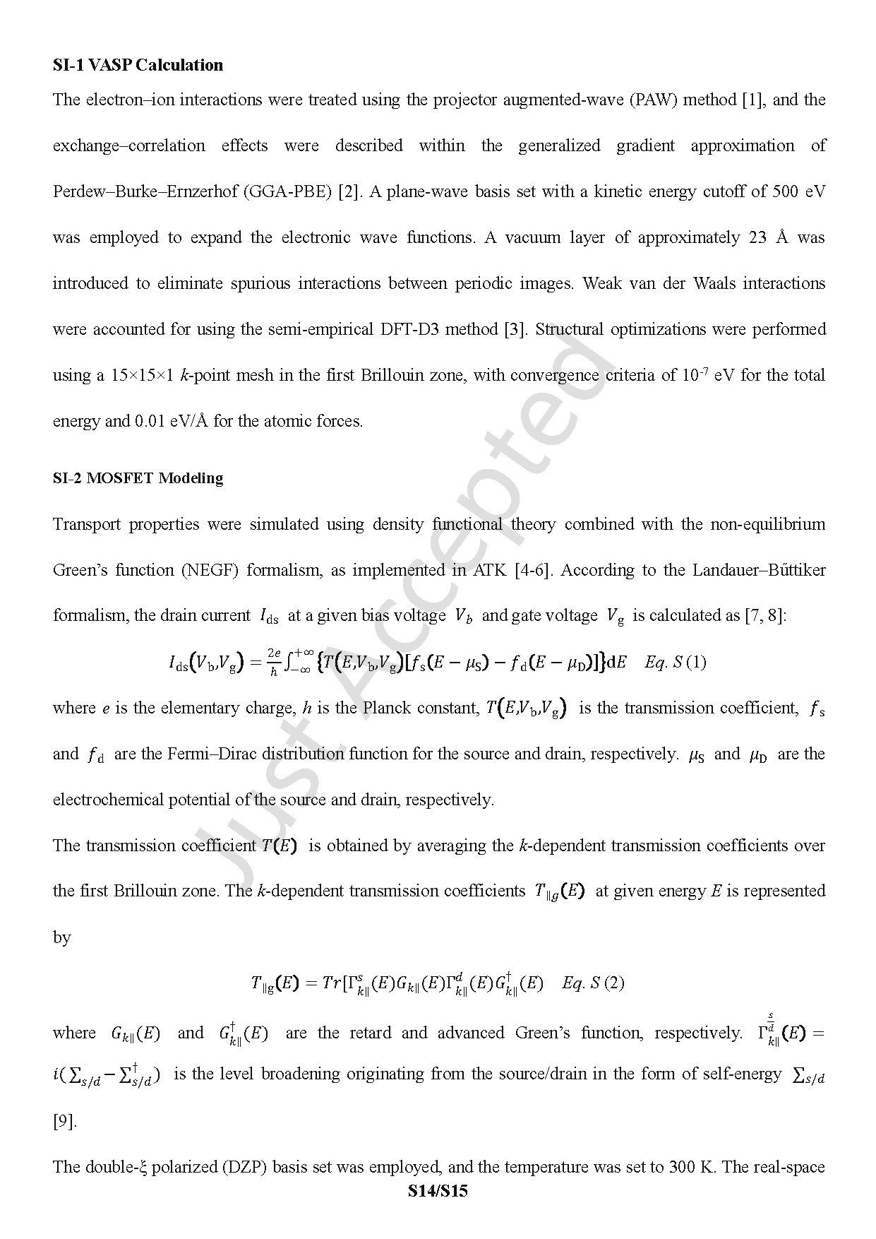
②Taking fully doped devices as benchmarks, first-principles NEGF simulations verify that LD devices balance high on-state current, reduced subthreshold swing and suppressed off tunneling leakage at the ultimate 1 nm gate length;
③The layer-confined transport mechanism is clarified: LD confines carriers within bottom conductive sublayers, reduces channel capacitance and lifts source-drain barrier to fundamentally suppress tunneling leakage;
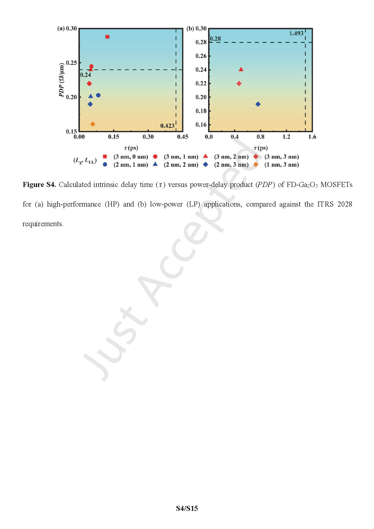
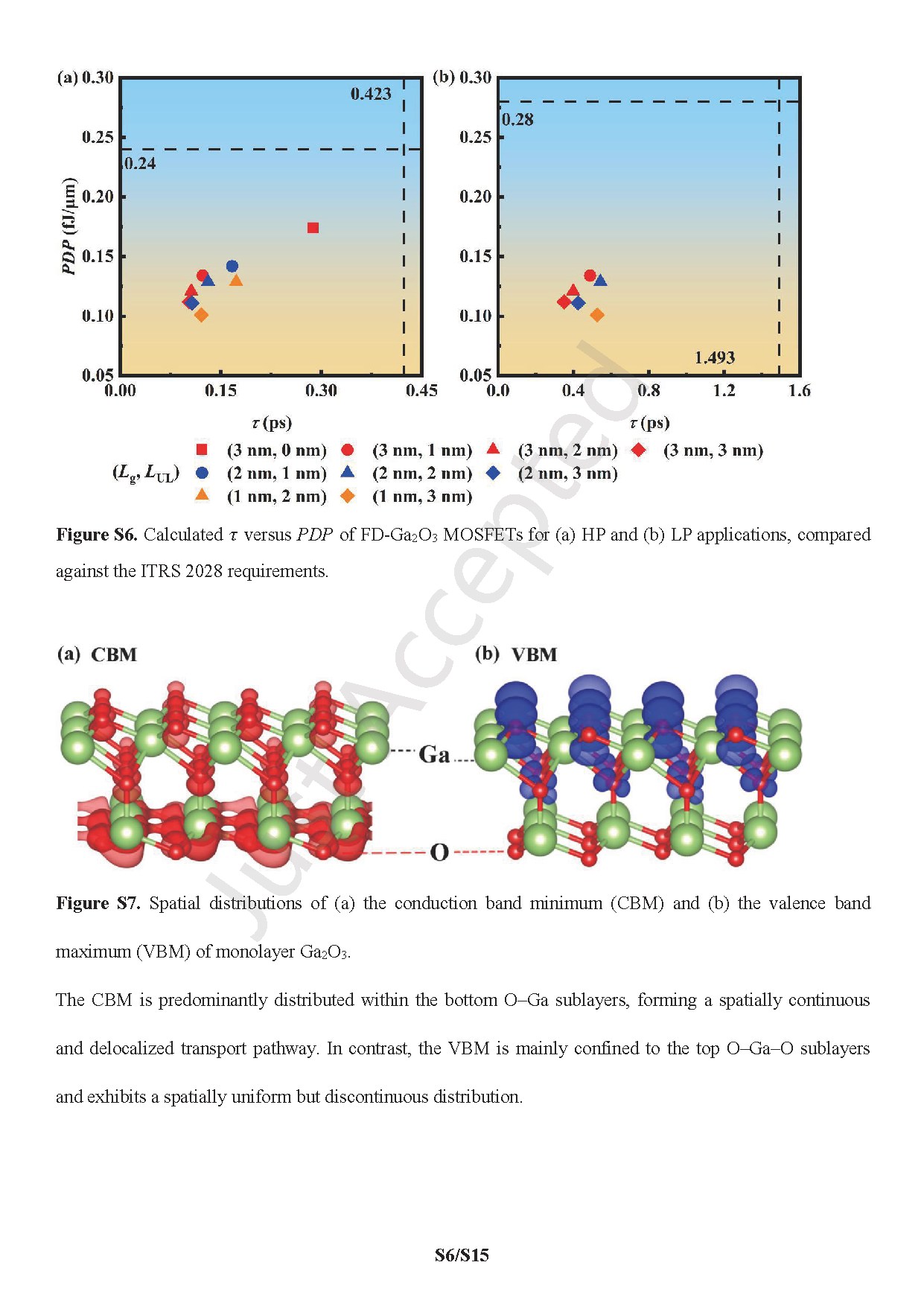
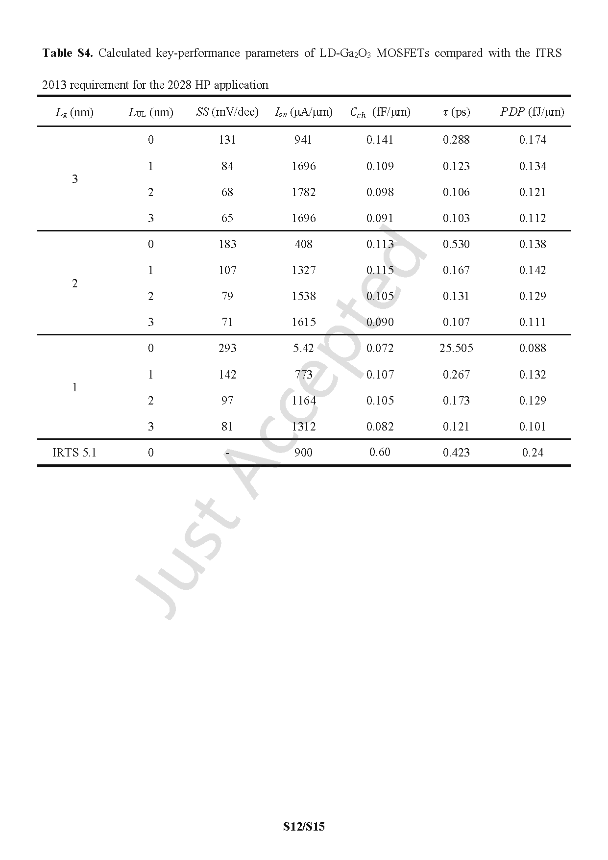
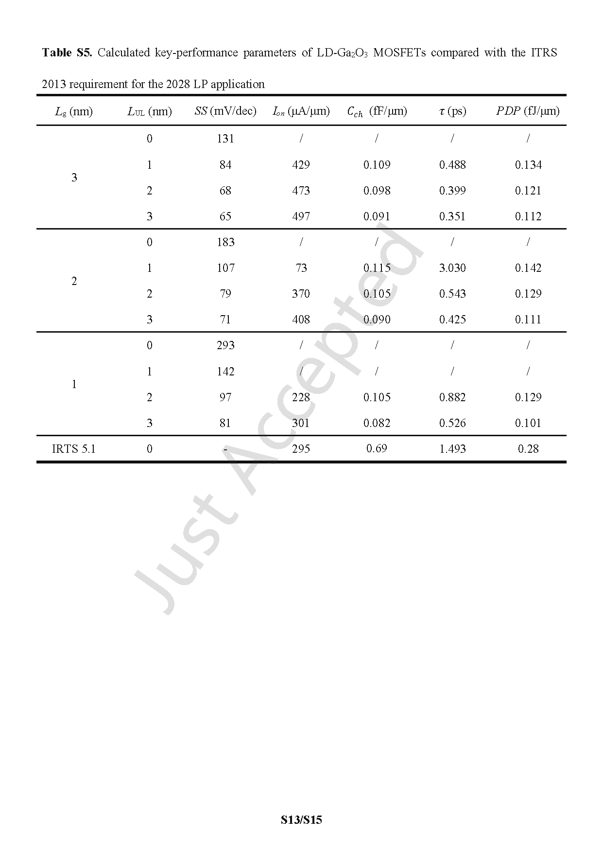
④Devices with multiple gate lengths (3 / 2 / 1 nm) and underlap widths satisfy both HP and LP ITRS standards, with overall performance superior to most reported 2D monolayer transistors;
⑤This layer-selective doping paradigm is generalizable to various vertically separated 2D asymmetric monolayers including MoSSe, Ga₂SSe and In₂Se₃.
Conclusion
In conclusion, we have proposed and systematically demonstrated an atomic-layer-selective source/drain (S/D) doping strategy to overcome the fundamental trade-off between carrier injection and gate electrostatic control in sub-3 nm monolayer MOSFETs. An atomic-layer-selective doping scheme is introduced for 2D asymmetric monolayer MOSFETs, in which n-type dopants are selectively incorporated into CBM-dominated regions to enhance electron transport while preserving the intrinsic conduction characteristics of the channel. By exploiting the intrinsic layer-resolved electronic structure of monolayer Ga₂O₃, where conduction-band electrons are confined to the bottom Ga-O sublayers, the locally doped (LD) design selectively enhances carrier injection within the conducting sublayers while preserving the intrinsic character of the remaining layers. Quantum transport simulations reveal that, compared with conventional fully doped (FD) devices, LD-Ga₂O₃ MOSFETs maintain competitive driving currents for both high-performance and low-power applications, while exhibiting substantially improved gate control. This is reflected in reduced subthreshold swing, suppressed off-state leakage, and lower channel capacitance, arising from layer-confined carrier transport that limits channel charge accumulation. At the ultimate 1 nm scaling limit, LD devices simultaneously deliver high on-state current and robust gate electrostatic control, outperforming or matching previously reported monolayer MOSFETs in both current drive and subthreshold characteristics. Beyond Ga₂O₃ atomic-layer-selective doping defines a materials-guided design paradigm applicable to two-dimensional asymmetric monolayers (e.g., MoSSe, Ga₂SSe, and In₂Se₃) featuring spatially separated carrier distributions, offering a viable pathway to extend transistor scaling beyond conventional electrostatic limits.
Project Support
This work is supported by the Natural Science Foundation of Chongqing (cstc2021jcyj-msxmX0524), the National Natural Science Foundation of China (22162025), the collaborative research project of Chongqing SanXia University of Science and Technology (2105/09924803n), and the reform program of Chongqing Municipal Education Commission (223310).
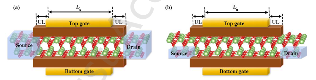
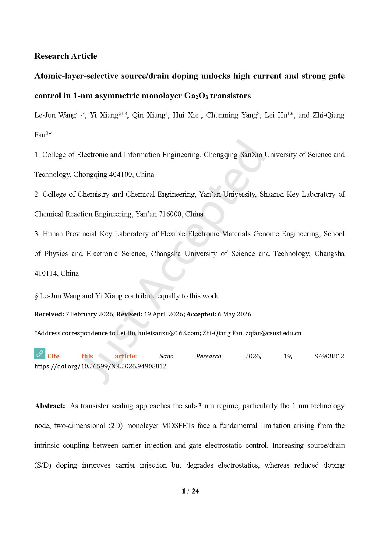
Figure 1 (a) Schematic of fully doped Ga₂O₃ transistor; (b) Schematic of atomic-layer-selective locally doped Ga₂O₃ transistor. Red spheres denote oxygen atoms and green spheres denote gallium atoms
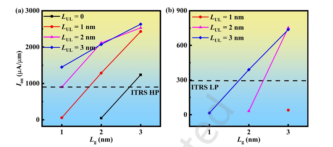
Figure 2 (a) Calculated on-current of fully doped devices for high-performance applications versus gate length; (b) Calculated on-current of fully doped devices for low-power applications versus gate length, dashed lines represent ITRS target values
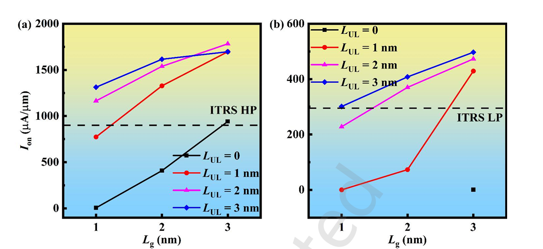
Figure 3 (a) On-current curves of locally doped devices under HP conditions; (b) On-current curves of locally doped devices under LP conditions
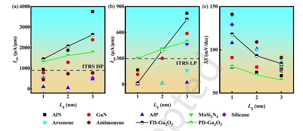
Figure 4 (a) Benchmark of HP on-current against reported n-type monolayer MOSFETs; (b) Benchmark of LP on-current; (c) Comparison of subthreshold swing values
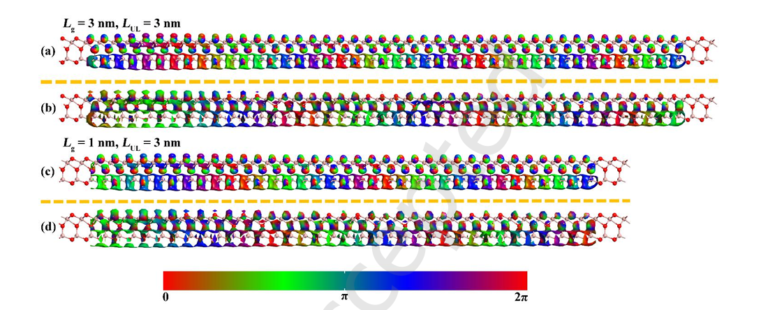
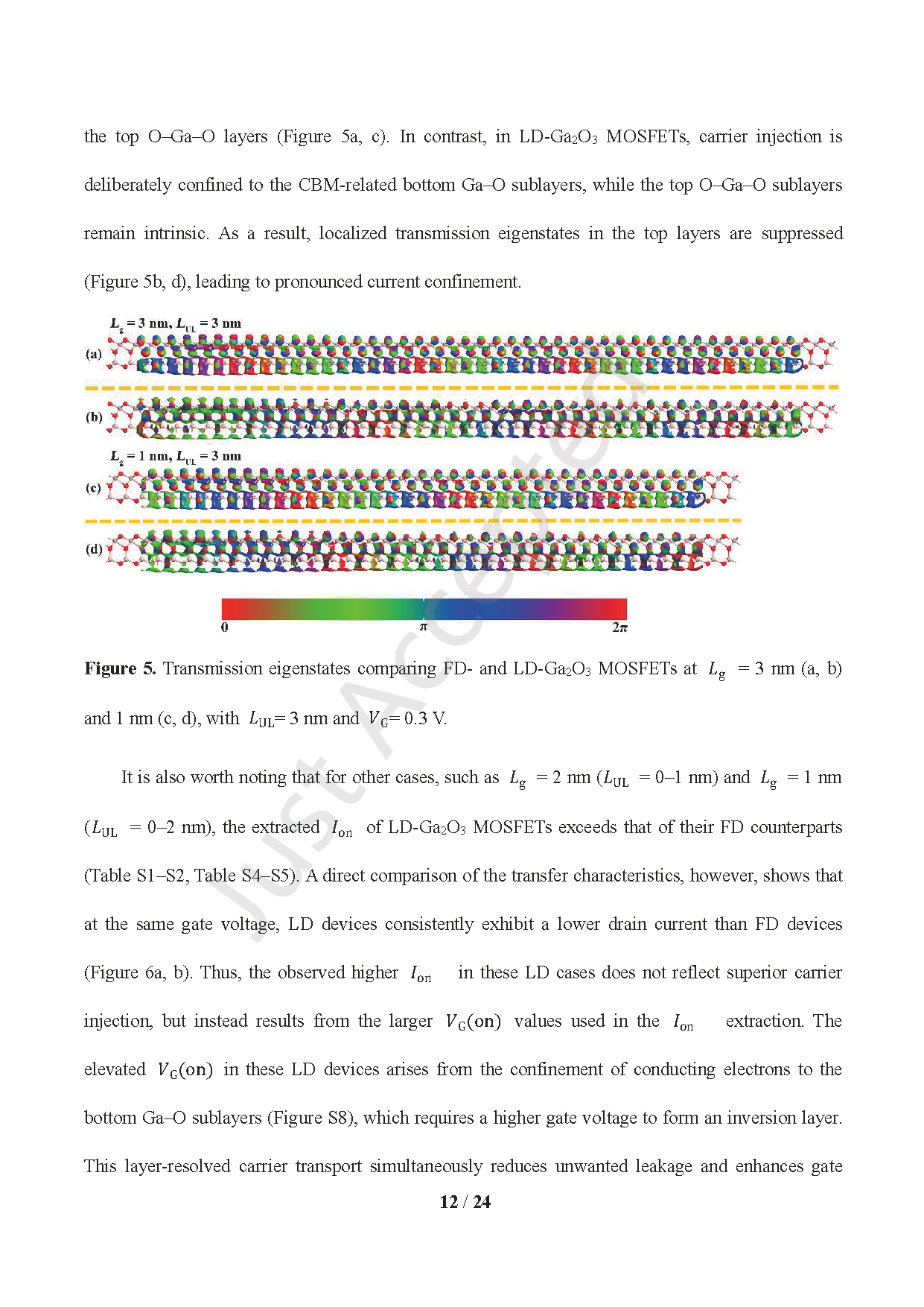
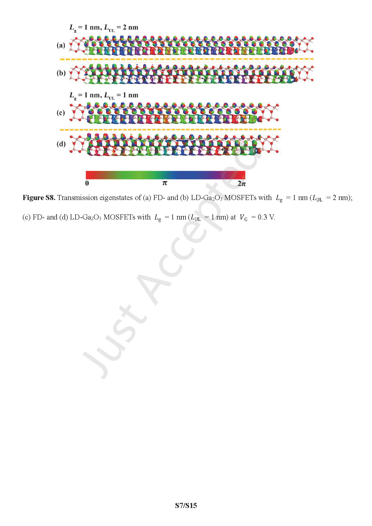
Figure 5 Transmission eigenstate distribution of fully doped and locally doped transistors at Lg = 3 nm, LUL = 3 nm and Lg = 1 nm, LUL = 3 nm
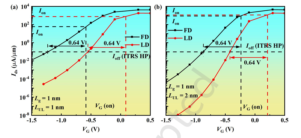
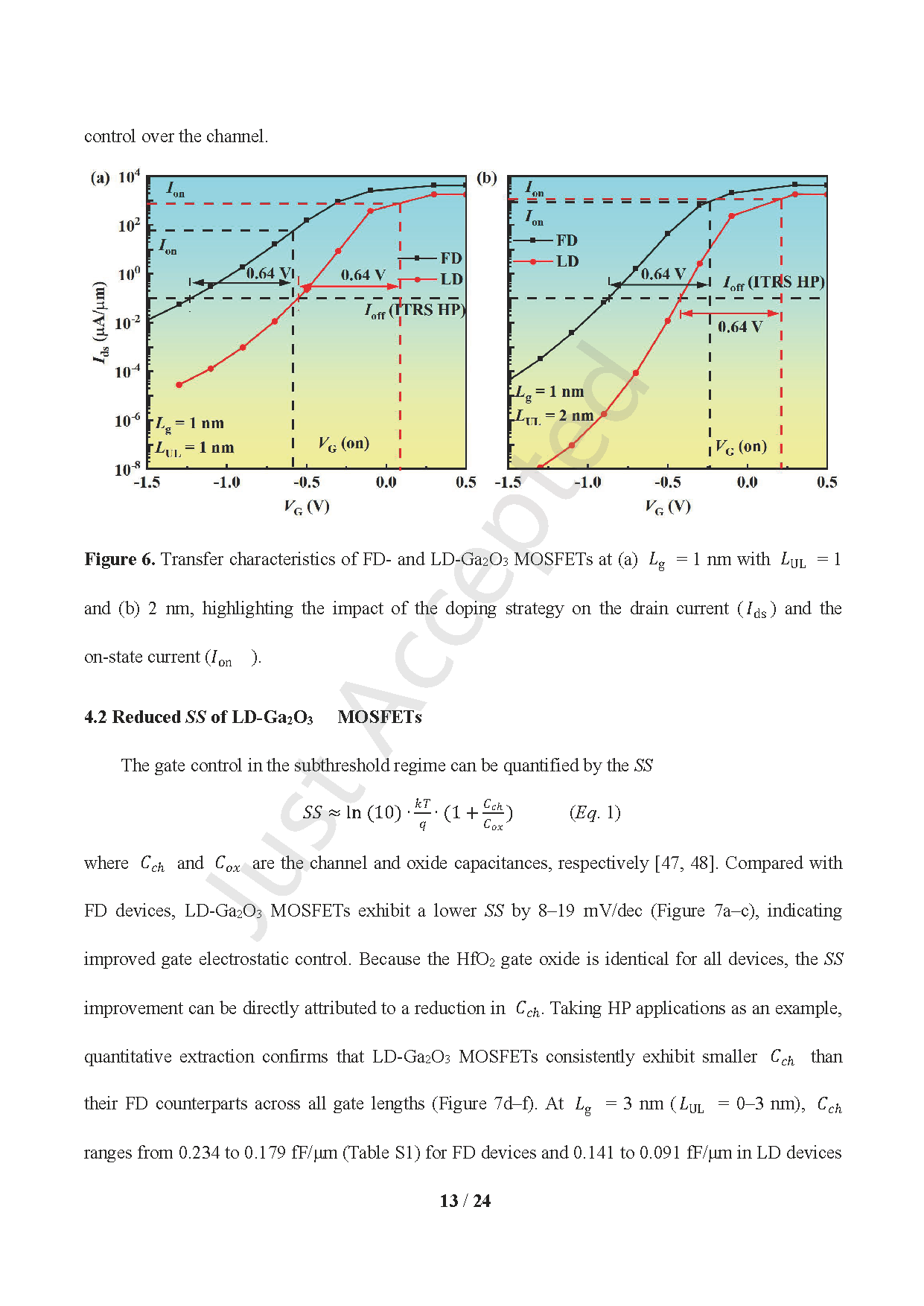
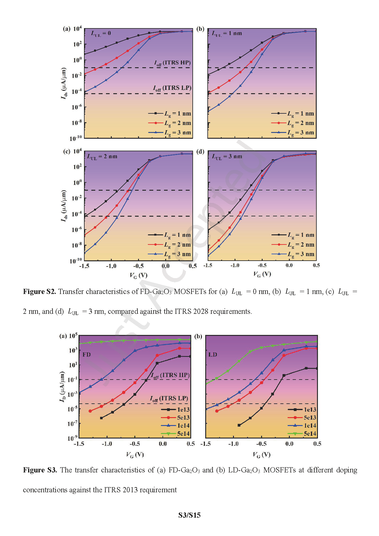
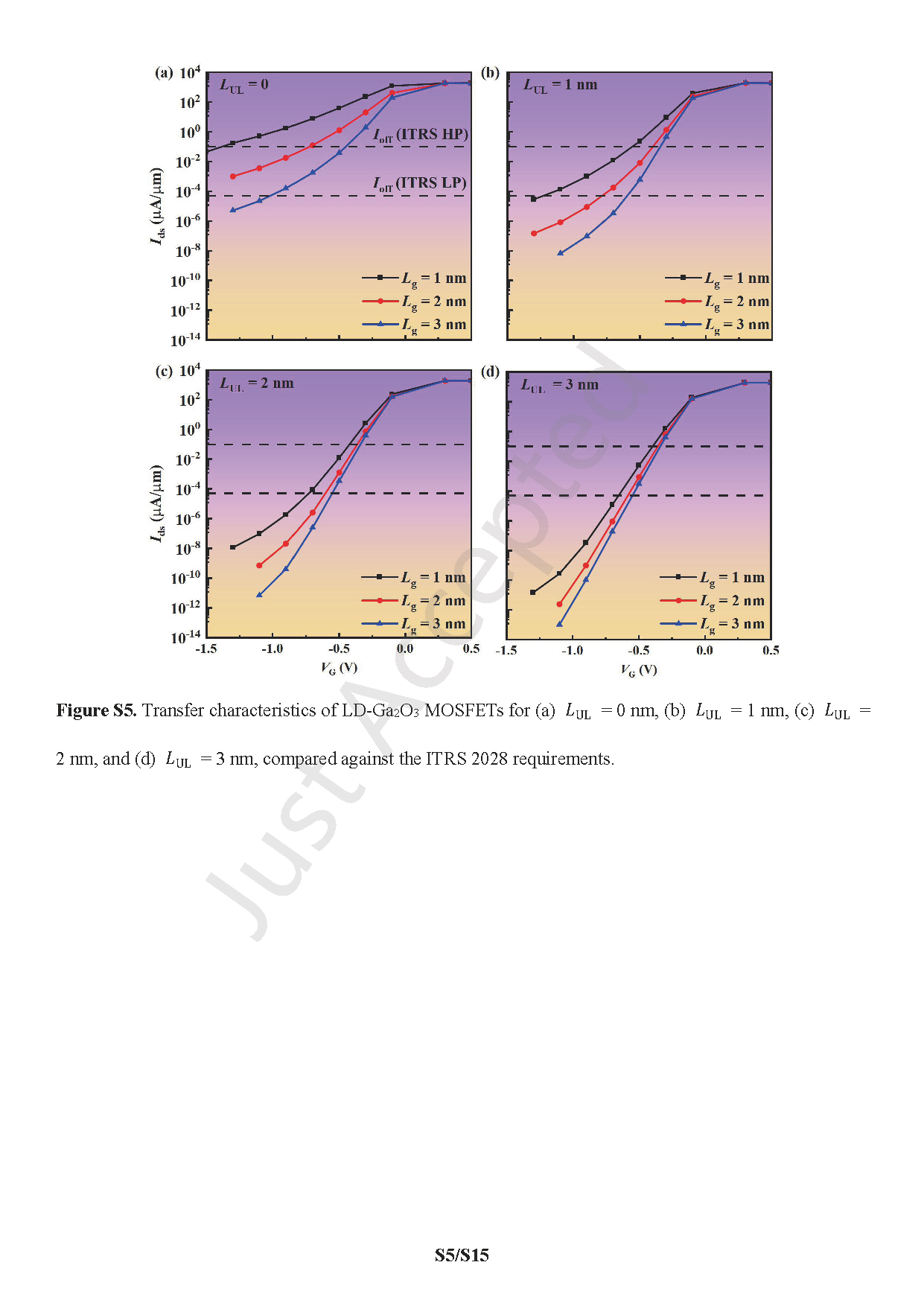
Figure 6 Transfer characteristic comparison of FD and LD devices at Lg = 1 nm with different underlap lengths
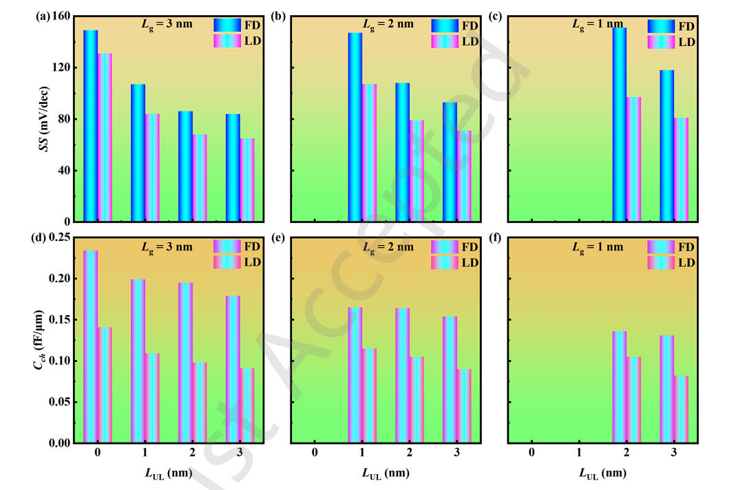
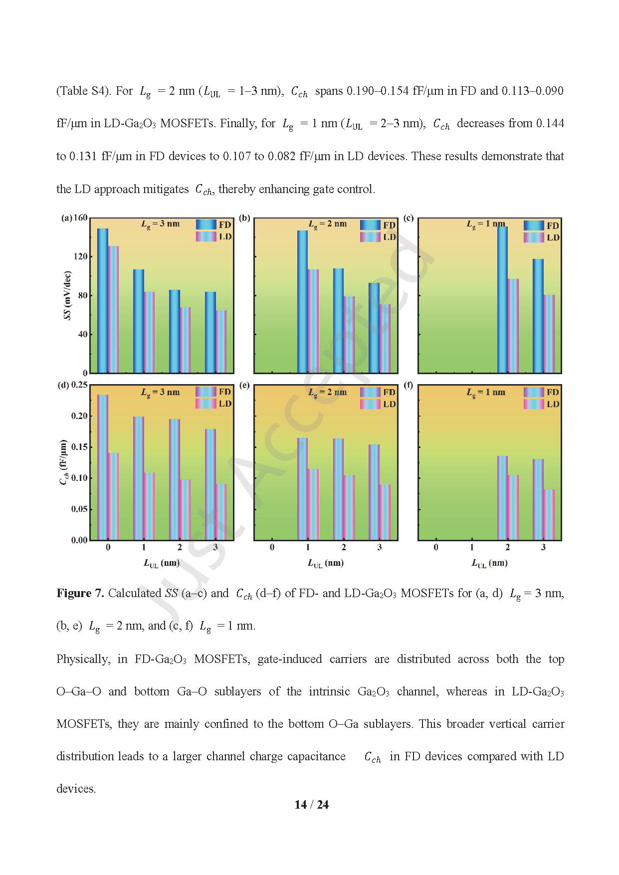
Figure 7 Column comparison of subthreshold swing and channel capacitance for FD and LD devices under varied gate lengths
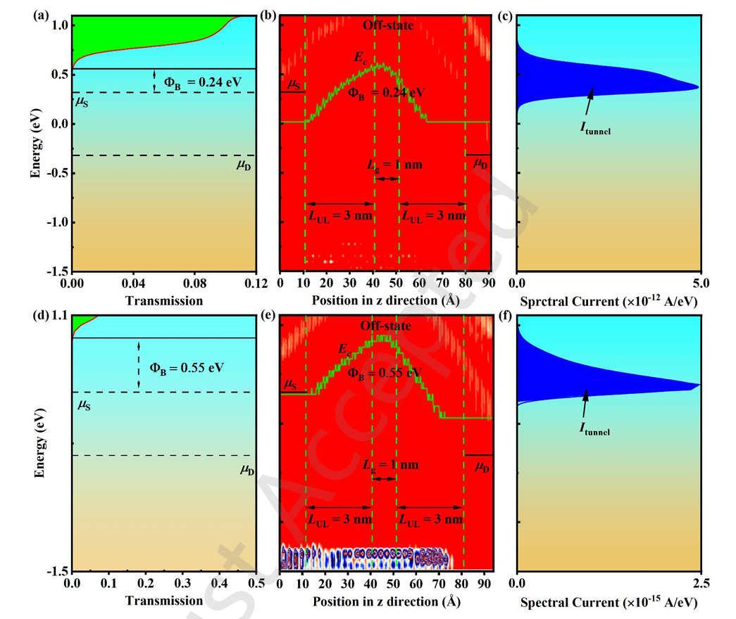
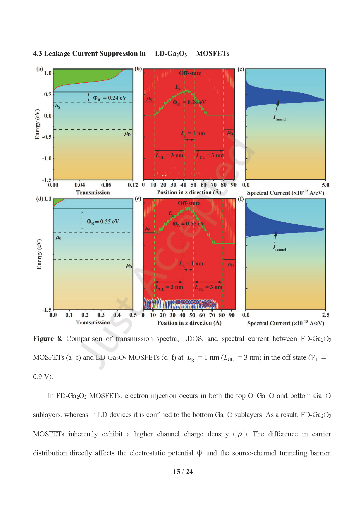
Figure 8 Comparison of transmission spectra, local density of states and spectral current between FD and LD devices under off-state bias
DOI:
doi.org/10.26599/NR.2026.94908812
Instruction
Official Account

Cooperation
Top
