


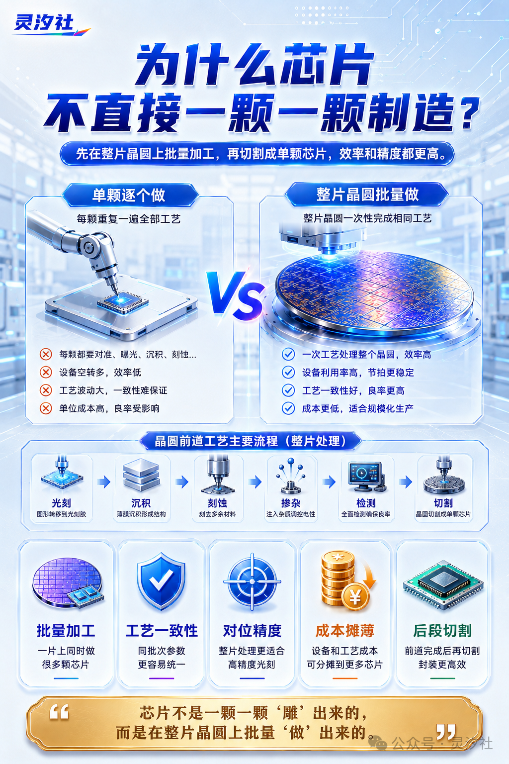
Many people associate chips directly with the small, black components found in electronic devices. However, in actual manufacturing, chips are not produced individually from the outset; instead, they are fabricated in batches on entire wafers. In essence, a wafer serves as the "foundation" of chip manufacturing.
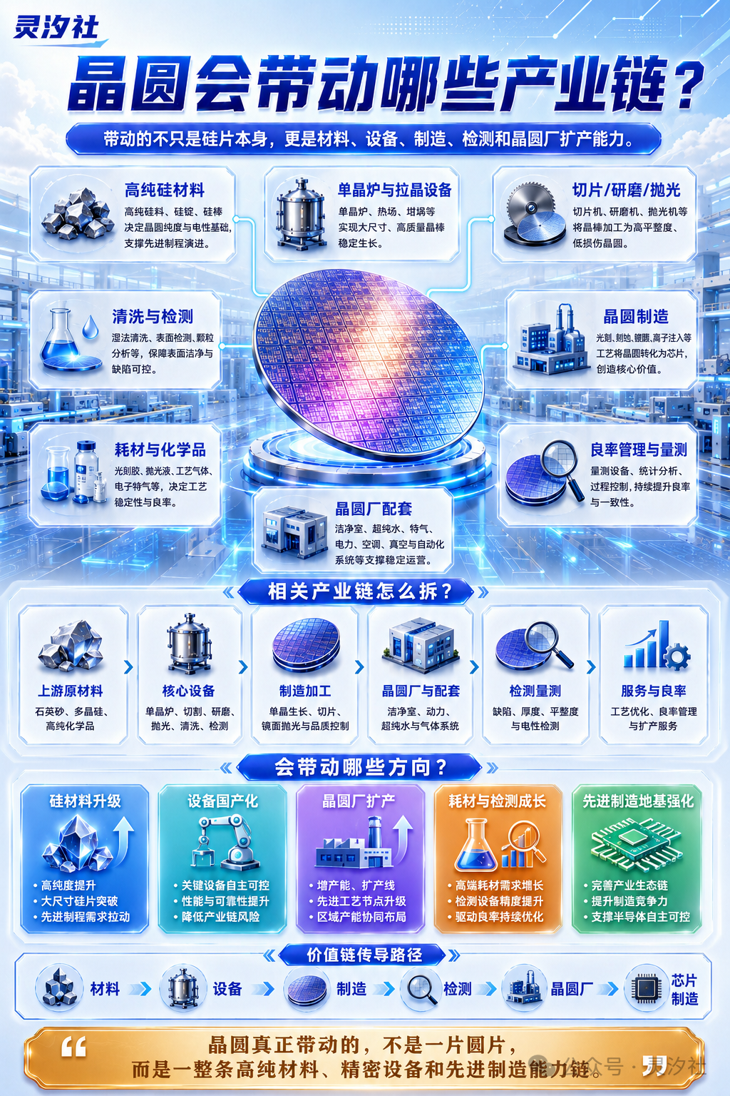
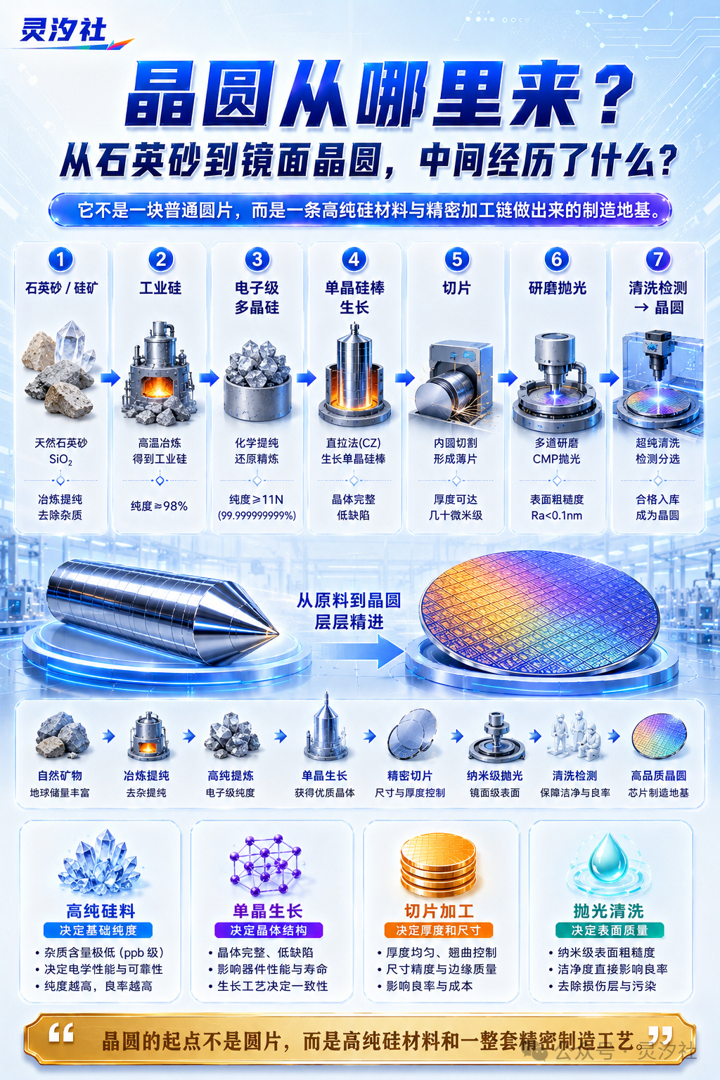
Wafers are typically crafted from high-purity silicon. Through a series of processes—including single-crystal growth, slicing, grinding, polishing, cleaning, and inspection—they are transformed into circular silicon substrates characterized by extreme purity, flatness, and stability.
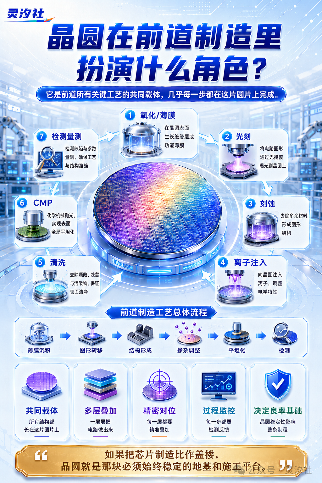
Why are the requirements so stringent? Because subsequent fabrication steps, such as photolithography, etching, thin-film deposition, ion implantation, chemical mechanical polishing (CMP), and inspection, are all performed on this substrate. Even trace amounts of impurities, particles, scratches, warpage, or variations in thickness can lead to pattern misalignment, thereby compromising chip performance and manufacturing yield.
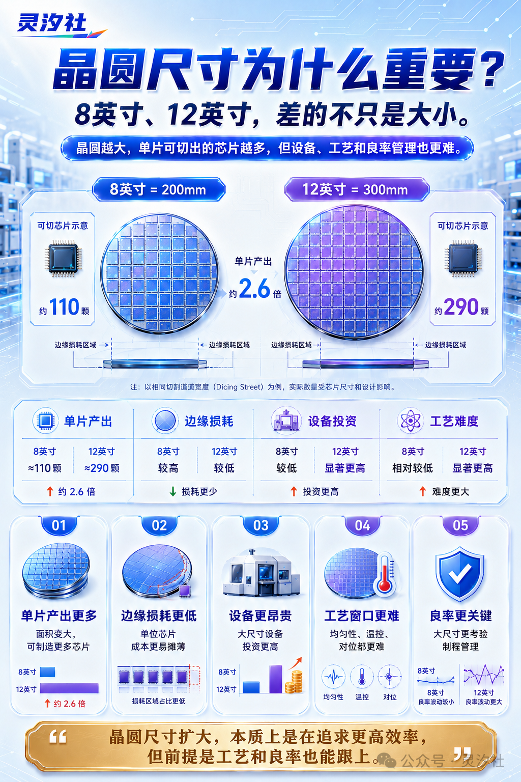
Wafer size is equally critical. The transition from 8-inch to 12-inch wafers is not merely a matter of diameter; it reflects significant differences in production throughput, capital investment, process complexity, and yield control. Larger wafers allow for a higher number of chips per unit, yet they demand even higher standards for equipment precision, material quality, thermal control, surface uniformity, and defect management.
Ultimately, the true value of a wafer lies not in its circular shape, but in its ability to serve as a sufficiently clean, flat, and stable platform for semiconductor fabrication. Stable chip manufacturing is impossible without reliable wafers. The first hurdle in chip manufacturing actually begins with this seemingly simple circular piece of material.

Instruction
Official Account

Cooperation
Top
