


Researchers from the Beijing Institute of Technology and Guangxi University and University of Oslo have published a dissertation titled " On the Structural and Optical Properties of Cerium Doped Ga2O3 Films after High-Temperature Annealing " in Optical Materials.
Background
Gallium oxide (Ga₂O₃) is a promising ultra-wide bandgap semiconductor with five polymorphic phases. The monoclinic β-Ga₂O₃ possesses the best thermal and chemical stability with a bandgap of approximately 4.9 eV, and it has been widely applied in power electronic devices, deep ultraviolet photodetectors, phosphors, gas sensors, photocatalysts and scintillators. As an indirect bandgap semiconductor, β-Ga₂O₃ shows low efficiency of intrinsic band-edge radiative recombination, and its luminescence is mainly derived from electronic transitions between energy levels of native point defects including oxygen vacancies, interstitial gallium, gallium vacancies, Ga-O divacancies and self-trapped holes.
Rare earth ions with unique electronic structures are commonly used as dopants to modulate the optoelectronic properties of semiconductors. Cerium (Ce), a typical rare earth element, mainly exists in two valence states of Ce³⁺ and Ce⁴⁺ in materials. The 5d→4f optical transition of Ce³⁺ generates characteristic blue emission, while Ce⁴⁺ is generally optically inactive. At present, multiple methods such as floating zone method, pulsed laser deposition, Czochralski method, spray pyrolysis and electrospinning have been used to synthesize Ce-doped Ga₂O₃, and their scintillation, luminescence and photocatalytic properties have been investigated.
Magnetron sputtering is an important technique for preparing high-quality semiconductor thin films. Most previous studies focused on the properties of Ce-doped Ga₂O₃ annealed at conventional temperatures, while the fundamental research on microstructure evolution, defect characteristics and optoelectronic performances of the materials after high-temperature annealing (above 900 ℃) is still insufficient. In this work, Ce-doped β-Ga₂O₃ thin films with different doping concentrations were fabricated by magnetron sputtering. The effects of annealing temperature, annealing atmosphere and Ce doping content on structural, optical and photoelectric detection properties of the thin films were systematically studied. The research results provide experimental basis for the further application of Ga₂O₃-based photonic and optoelectronic devices.
Abstract
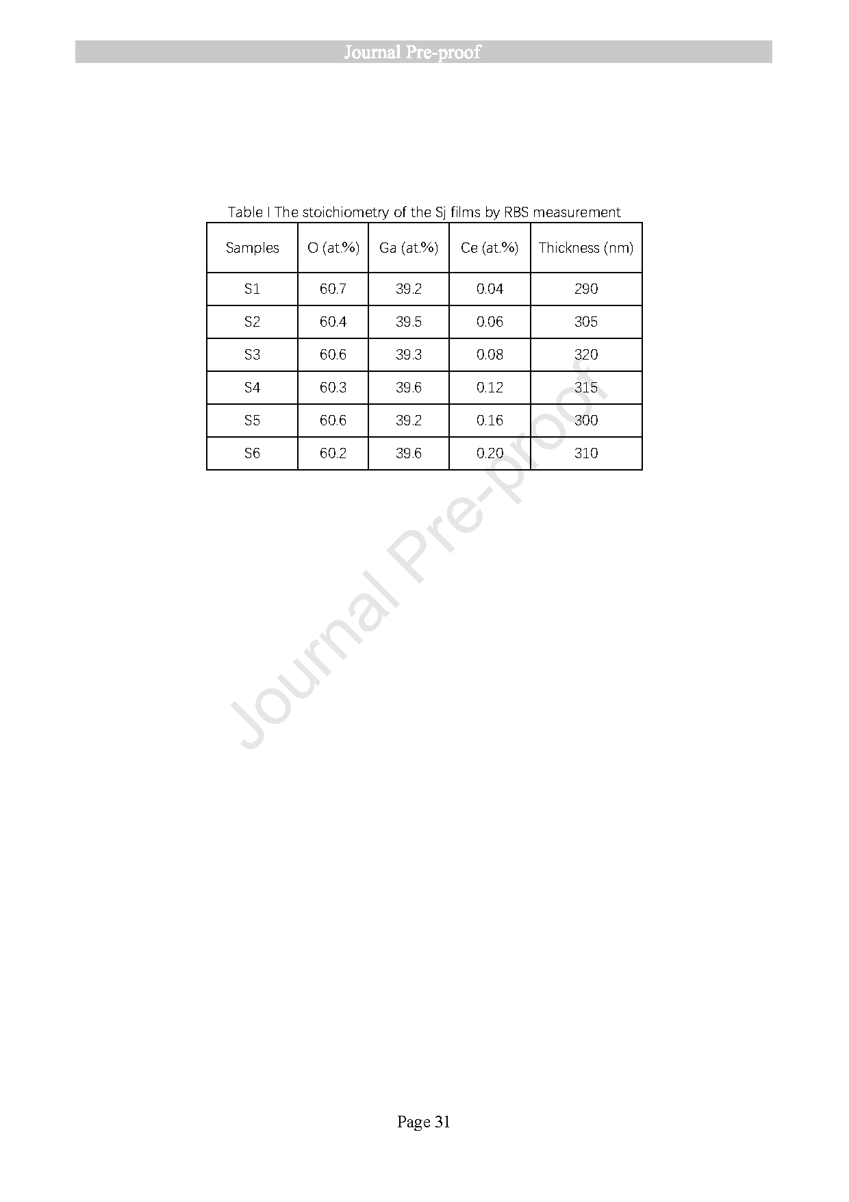
In this work, we investigated the structural and optical properties of cerium (Ce) doped β-Ga₂O₃ thin films, which were deposited by magnetron sputtering and subjected to high-temperature annealing. The Ce doping concentration was varied systematically from 0.04 at.% to 0.20 at.%. The as-deposited films were all amorphous, with topography that changed with Ce concentration. Crystallization of the films occurred upon annealing, and grain growth of β-Ga₂O₃ nanocrystals was observed via X-ray diffraction. For samples annealed at 1100 °C in air ambience, X-ray photoelectron spectroscopy (XPS) indicated the presence of both Ce³⁺ and Ce⁴⁺ ions, and charge states of Ga and oxygen favoring oxygen-vacancies and Ga⁺ defects having similar concentration dependence on the Ce doping level. The optical bandgaps of the annealed films are larger than that of β-Ga₂O₃ (~ 4.9 eV), which is attributed to Al from the Al₂O₃ substrate diffusing into the films during the high-temperature annealing. For samples annealed at 1100 °C in nitrogen, photoluminescence (PL) was significantly stronger than that of samples annealed in air; In both environments, PL intensities exhibited a similar trend with Ce doping concentrations, increasing for 0 to 0.06 at.%, and from there drastically decreasing. The variation in PL intensities correlates with the changes in oxygen-vacancies inferred from XPS analysis. Besides the emission bands from the Ga₂O₃ matrix, the PL spectra of Ce-doped samples show bands associated with optical transitions 5d (²D) → ²F₅/₂ and 5d (²D) → ²F₇/₂ of Ce³⁺. The photo-electric properties of the films for solar-blind detectors application were also examined. This work may contribute to the broader application of Ga₂O₃ based photonics and photo-electronics.
Highlights
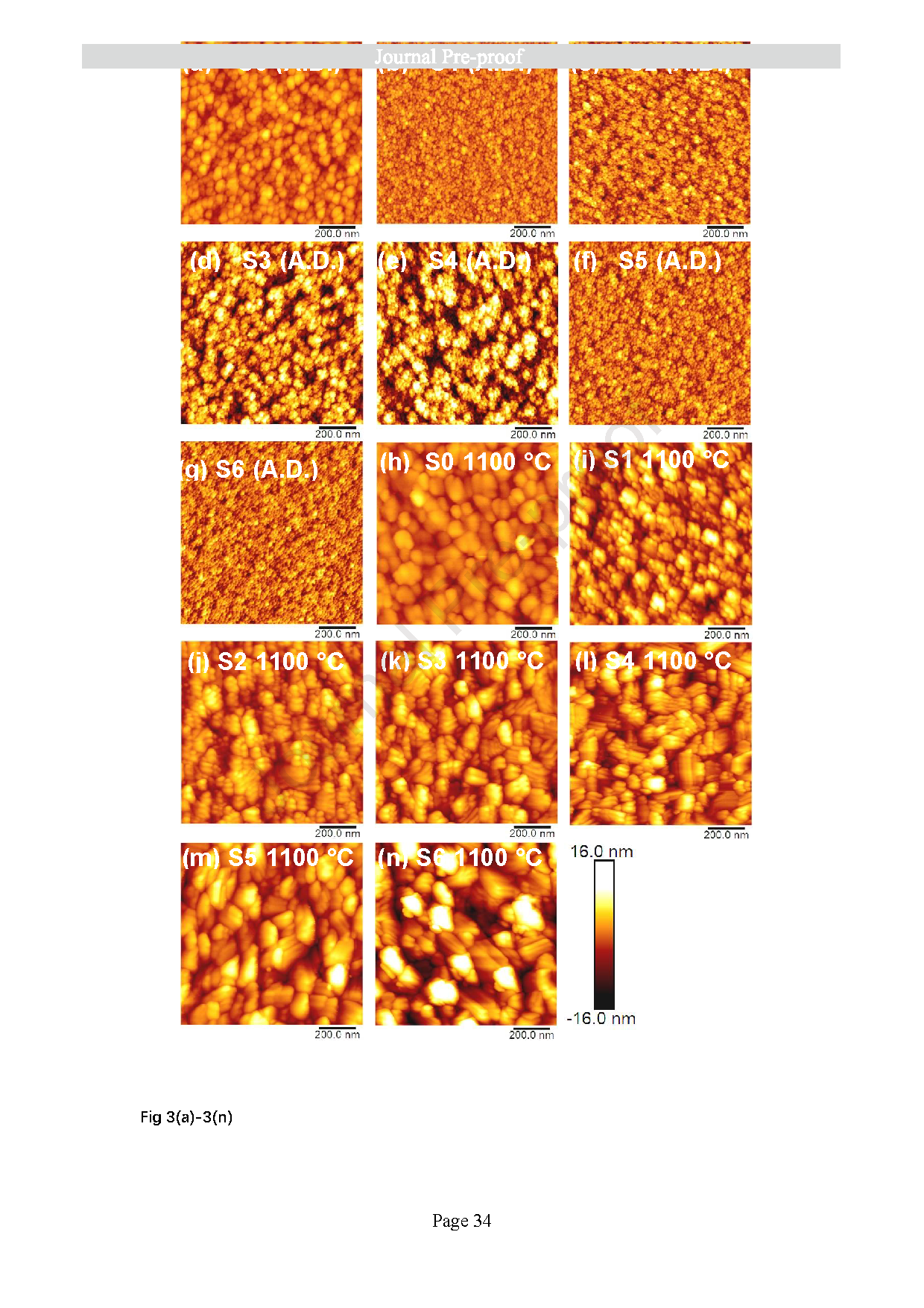
Sputter deposition yielded amorphous Ga₂O₃with topography that depends upon Ce doping concentration in the range 0.04 at.% to 0.20 at.%.
High temperature annealing yields crystallization, and photoluminescence from Ce³⁺and the common emission bands from β-Ga₂O₃ involving native defects.
The emission intensity is higher for annealing in an ambient of nitrogen than it is for air.
The photo-electric properties of the films for solar-blind detectors application were also examined.
Conclusion
This study investigated the effects of slight Ce-doping on the structure, optical and photoelectric properties of β-Ga₂O₃ films, following high temperature annealing both in air and N₂ atmospheres. High temperature annealing from 800 to 1100 °C, significantly improved the quality of the films, as evidenced by enhanced crystalline structure observed through XRD analysis and surface morphology characterized by using AFM.
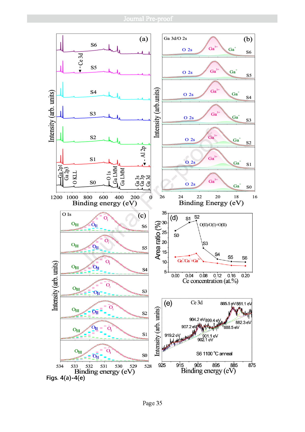
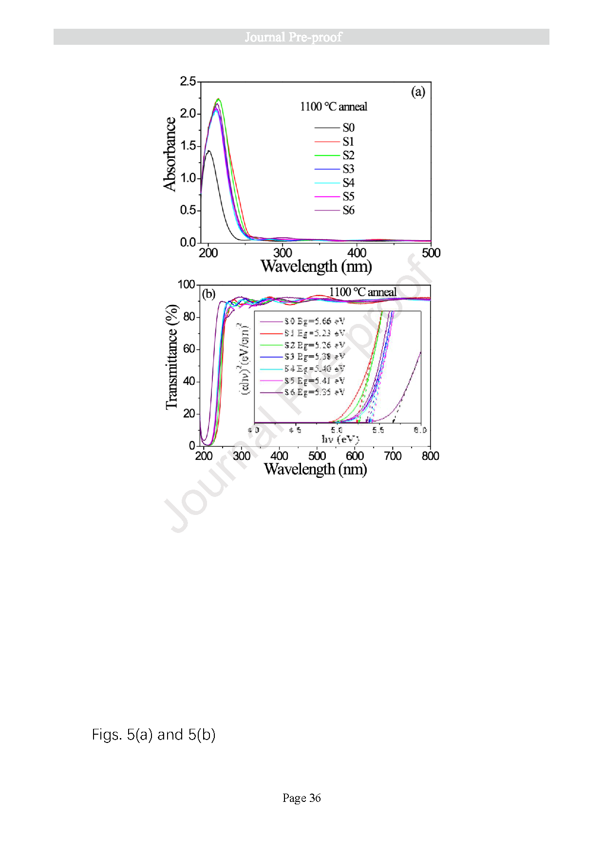
XPS results indicated the presence of both Ce³⁺ and Ce⁴⁺ ions in the films, as well as changes in defect concentrations, including oxygen-vacancies and Ga⁺ defects, which exhibit similar trends with increasing Ce concentration. Additionally, for films annealed at 1100 °C annealing in air, the UV-vis spectra demonstrated high optical transmittance of approximately 90%. The annealing caused diffusion of Al from the Al₂O₃ substrate to create β-(AlₓGa₁₋ₓ)₂O₃ resulting in a higher bandgap than for β-Ga₂O₃. Ce doping resulted in smaller optical band gaps as determined by the Tauc method compared to the undoped samples while all larger than for β-Ga₂O₃.
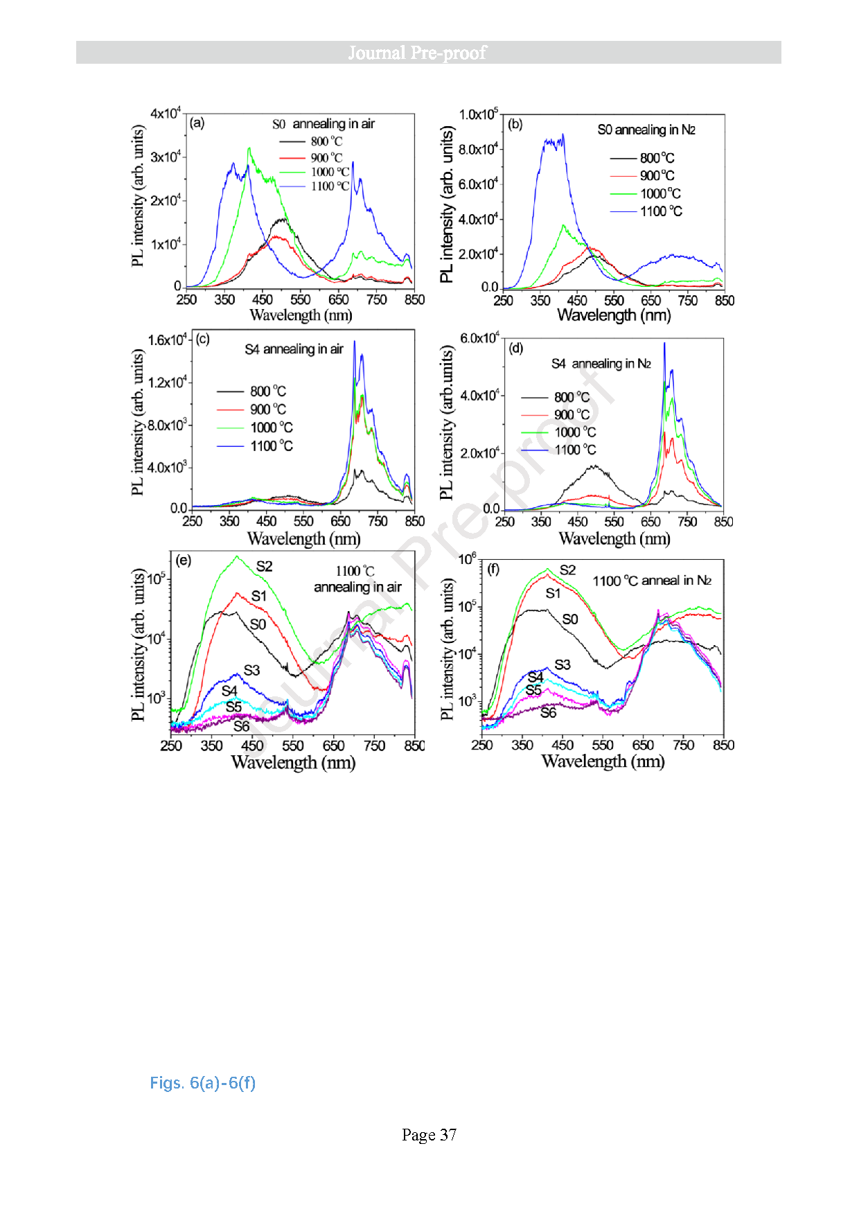
PL analysis revealed prominent UV−green band alongside a wide red emission band. The intensities of the UV−green emissions initially increased with Ce doping before decreasing significantly, while the red emission band became dominant at higher Ce concentration. Furthermore, PL intensities were enhanced for samples annealed in N₂ compared to those of annealed in air, likely due to reduced defect concentrations associated with oxygen vacancies in the latter. The PL spectra was modelled by Gaussian peak fitting with multiple emission bands, including transitions associated with Vo and Ce ions.
In terms of photo-electrical performance, the devices made with the films exhibited ohmic contact characteristics, with photocurrents initially increasing and then sharply declining with higher the Ce concentrations. The devices displayed strong stability and repeatability under repeated UV light exposure, as indicated by their photo-to-dark current ratios. The rise and decay times of the devices varied with Ce concentration, suggesting a correlation between Ce doping and the dynamic response of the films.
Overall, this research highlights the potential of Ce-doped β-Ga₂O₃ films for applications in photonic and photoelectric devices, particularly in solar-blind detectors. Future studies will aim to further elucidate the mechanisms underlying the observed optical and electrical properties, as well as explore additional doping strategies for enhanced performance.
Project Support
This work is supported by the National Natural Science Foundation of China No. 61775016. Prof. W. H. Sun thanks the support by the National Natural Science Foundation of China (No.62575079), High luminous efficiency and long life DUV LED technology (NO. AC22080003). We also thank the Analysis & Testing center of Beijing Institute of Technology for the great help in the XRD, SEM and UV-Vis experiments.
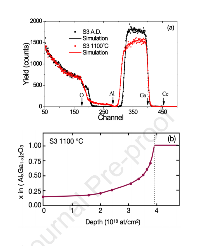
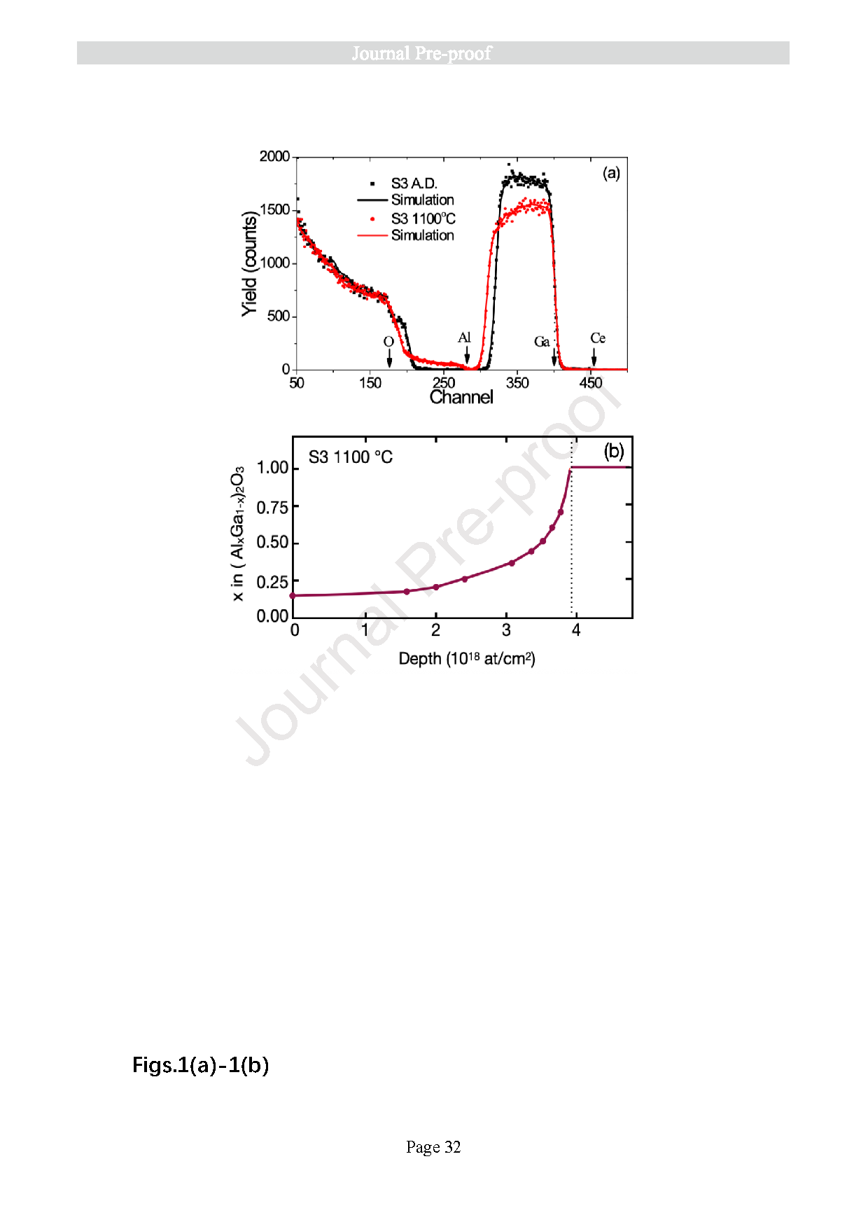
Fig. 1 (a) The RBS spectra of S3 samples A.D. and after annealing in air at 1100 °C along with their simulation curves. (b) The Al concentration profile in the annealed S3 film, with variable x in (AlₓGa₁₋ₓ)₂O₃ varying with depth from 0.14 at the surface to 1.
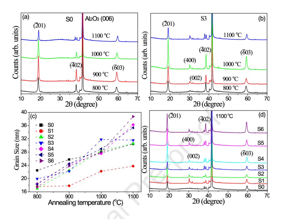
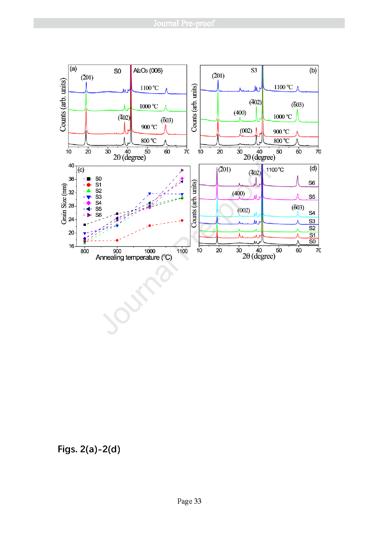
Fig. 2 The XRD diffractogram of (a) undoped Ga₂O₃ (S0) and (b) S3 samples after annealing in air at 800 °C, 900 °C, 1000 °C and 1100 °C respectively. (c) The average size of Ga₂O₃ nanocrystals of the Sⱼ (j=0,1,2,3,4,5,6) samples after annealing at the indicated temperatures. (d) The diffraction patterns of the Sⱼ samples after the identical 1100 °C annealing in air.
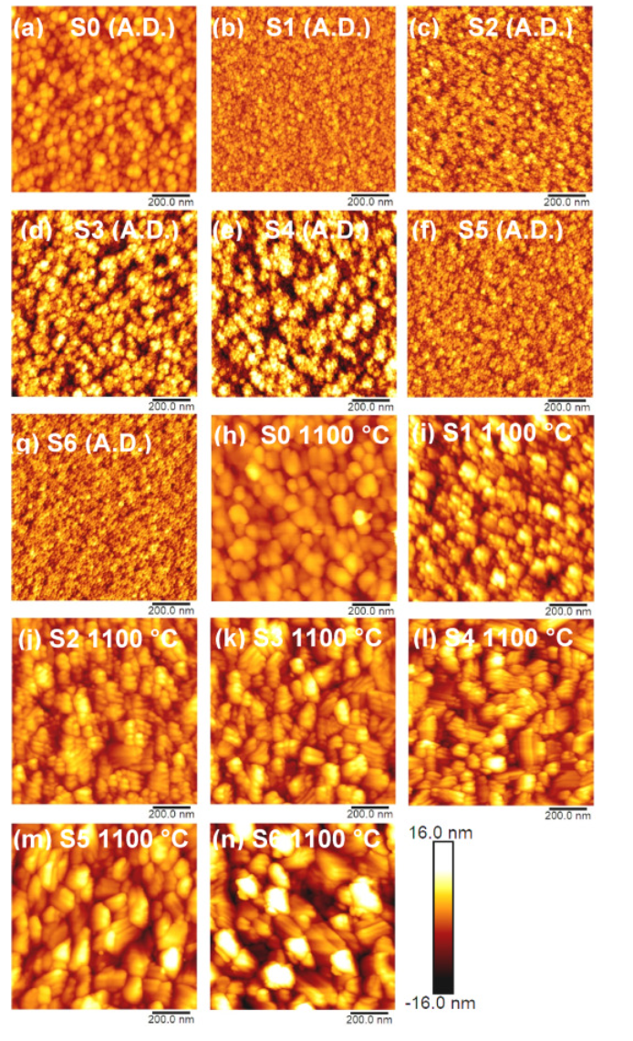
Fig. 3 (a)−(g) The AFM images of A.D. Sⱼ (j=0,1,2,3,4,5,6) samples. (h)-(n) The AFM images of the Sⱼ samples after annealing at 1100 °C in air.
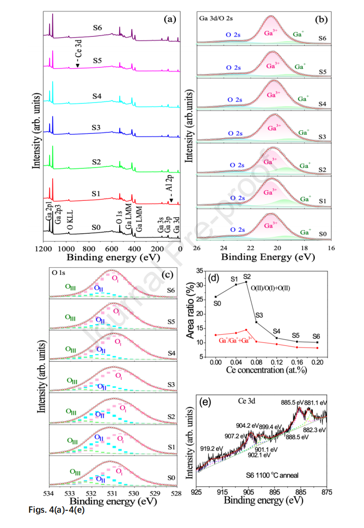
Fig. 4 The XPS spectra of Sⱼ (j=0,1,2,3,4,5,6) samples after annealing at 1100 °C in air. (a) The survey spectra, (b) the Ga 3d/ O 2s spectra and the simulation curves, (c) the O 1s spectra and the simulation curves. (d) The ratio of Ga⁺/(Ga³⁺+Ga⁺) and OⅡ/(OⅠ+OⅡ) in the Sⱼ samples. (e) The Ce 3d spectrum of S6 sample and the simulation curve.
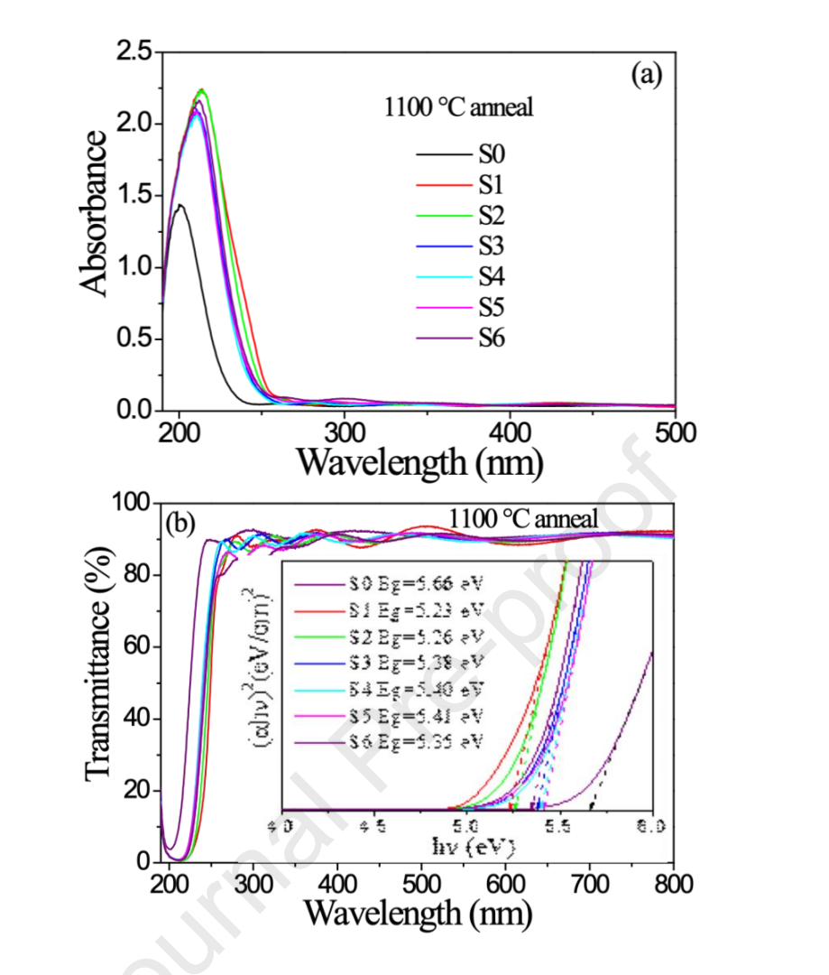
Fig. 5 (a) The absorption spectra and (b) transmission spectra of the Sⱼ (j= 0, 1, 2, 3, 4, 5, 6) samples after annealing at 1100 °C in air. The inset in Fig. 5 (b) is the Tauc plot and the obtained bandgaps of the Sⱼ samples.
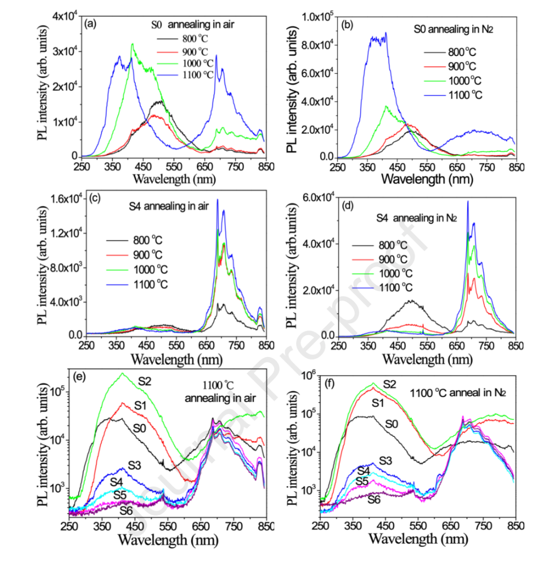
Fig. 6 (a) and (c) The PL spectra of the S0 and S4 samples after annealing in air, and (b) and (d) after annealing in N₂, at the indicated temperatures. Please notice the different scales. (e) and (f) The PL spectra of the Sⱼ samples after annealing at 1100 °C in air and N₂, respectively.
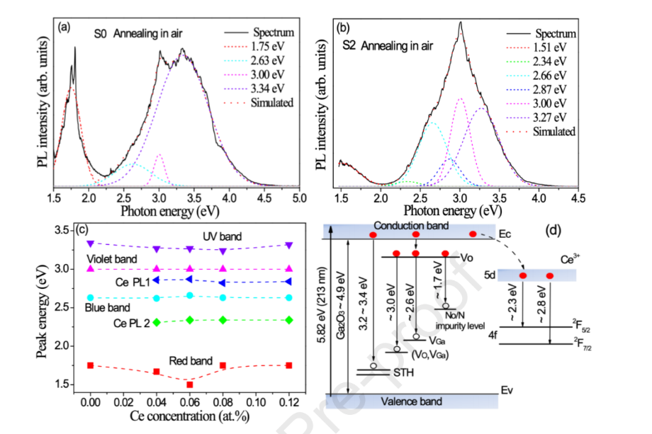
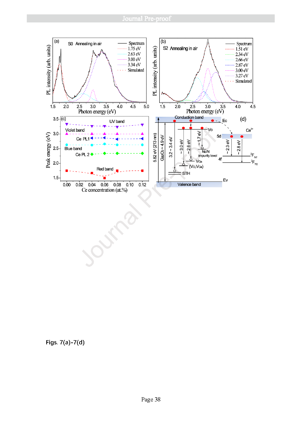
Fig. 7 Simulation of the PL spectra (a) S0 sample and (b) S2 sample after annealing at 1100 °C in air. The PL spectrum of S0 can be curve-fitted using four Gaussian bands with peak energy at around 3.34 eV, 3.00 eV, 2.63 eV and 1.75 eV, and the spectrum of S2 can be fitted using six Gaussian bands with peak energy at around 3.27 eV, 3.00 eV, 2.87, 2.66 eV, 2.34 eV and 1.51 eV, respectively. (c) The peak positions of the fitted Gaussian bands (including the two Ce emission bands, Ce PL1 and Ce PL2) of the S0-S4 samples. (d) The energy position of defect states in the bandgap of Ga₂O₃ with possible transition giving luminescence bands of the Sⱼ samples under the 213 nm laser excitation.
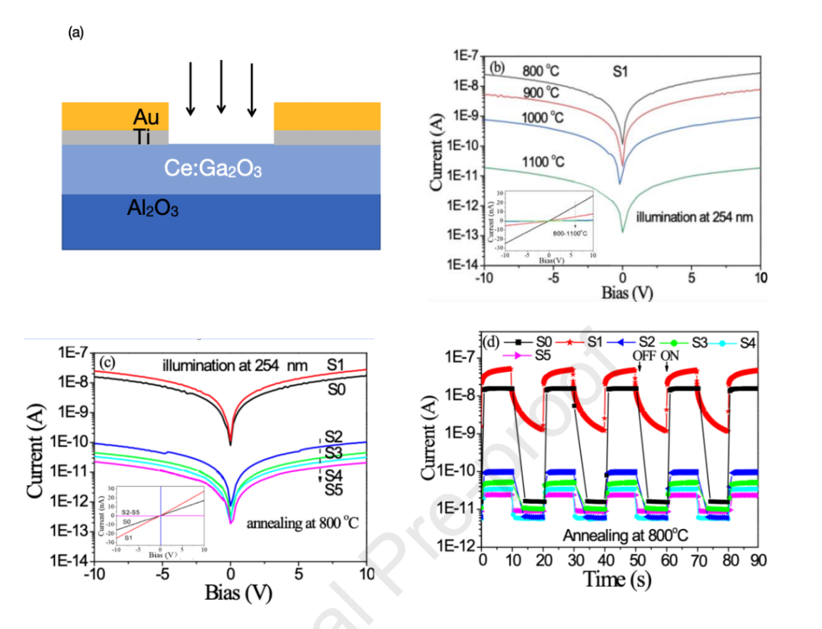
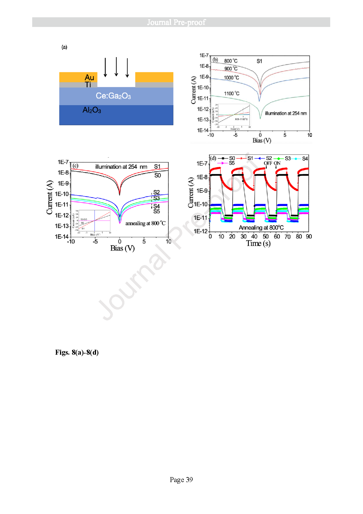
Fig. 8 (a) Schematic diagram of the MSM devices based on the Sⱼ (j=0,1,2,3,4,5) samples. (b) The I-V characteristic curves of S1 devices after annealing at the indicated temperatures and under a 254 nm LED illumination. The inset in Fig. 1 (b) shows the PL spectra of the S1 samples. (c) The I-V characteristic curves of Sⱼ devices after annealing at 800 °C in air and under the 254 nm LED illumination. The inset shows the PL spectra of the Sⱼ samples. (d) The switch on/off test performed for the Sⱼ devices after 800 °C annealing in air by applying a 10 V bias and under the 254 nm LED illumination.
DOI :
doi.org/10.1016/j.optmat.2026.118238



Instruction
Official Account

Cooperation
Top
