


Researchers from the Xi’an Jiaotong University have published a dissertation titled " Radiation damage and hardening via supercritical fluid process in Al2O3/β-Ga2O3 MOSCAPs: Insights from proton, Ta-ion, γ-ray, and neutron irradiation " in Applied Physics Letters.
Background
β-Ga₂O₃ devices have great application prospects in space extreme irradiation environments owing to their high threshold displacement energy, outstanding radiation detection and solar-blind photodetection capabilities. High-energy particles and rays induce complex radiation damage inside β-Ga₂O₃ devices via ionizing energy loss and non-ionizing energy loss. Previous investigations on radiation damage of β-Ga₂O₃ devices mainly focus on vertical Schottky barrier diodes, vertical pn junction diodes and planar metal–semiconductor–metal devices, whose damage origins are dominated by the radiation response of bulk β-Ga₂O₃ and metal-semiconductor interfaces.
The Al₂O₃/β-Ga₂O₃ MOS structure has been widely adopted in trench Schottky barrier diodes and MOS field-effect transistors, while systematic comparative researches on irradiation damage mechanisms of Al₂O₃/β-Ga₂O₃ metal–oxide–semiconductor capacitors (MOSCAPs) remain insufficient. Intrinsic defects such as oxygen vacancies Vₒ in Al₂O₃ layers dominate the radiation tolerance of Al₂O₃/β-Ga₂O₃ MOS devices; holes generated by ionization damage can be trapped by Vₒ and convert them into electron traps, which aggravate leakage current.
Conventional high-temperature annealing exhibits limited performance in passivating intrinsic defects. Low-temperature supercritical fluid (SCF) treatment can simultaneously passivate Vₒ in Al₂O₃ and heterojunction interface traps, reduce interfacial electric field and boost breakdown electric field, which is a promising radiation hardening strategy for β-Ga₂O₃ MOS devices. To date, no comprehensive study has systematically compared the distinct damage behaviors induced by proton, tantalum (Ta)-ion, γ-ray and neutron irradiation on Al₂O₃/β-Ga₂O₃ MOSCAPs, nor verified the radiation hardening effect of SCF pretreatment.
Abstract
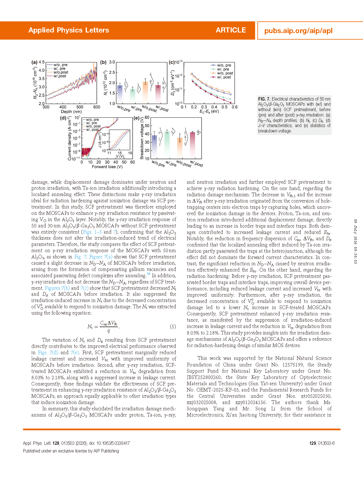
In this study, the degradation of Al₂O₃/β-Ga₂O₃ MOSCAPs under proton, tantalum (Ta)-ion, γ-ray, and neutron irradiation is systematically compared. The influence of key parameters on device performance was thoroughly investigated, including interface state density (Dit), border trap density (Nt) in the Al₂O₃ layer, and the net carrier concentration (ND−NA) in β-Ga₂O₃. Based on the elucidated irradiation damage mechanism, the potential of SCF pretreatment for achieving γ-ray irradiation hardening for Al₂O₃/β-Ga₂O₃ MOSCAPs was further explored.
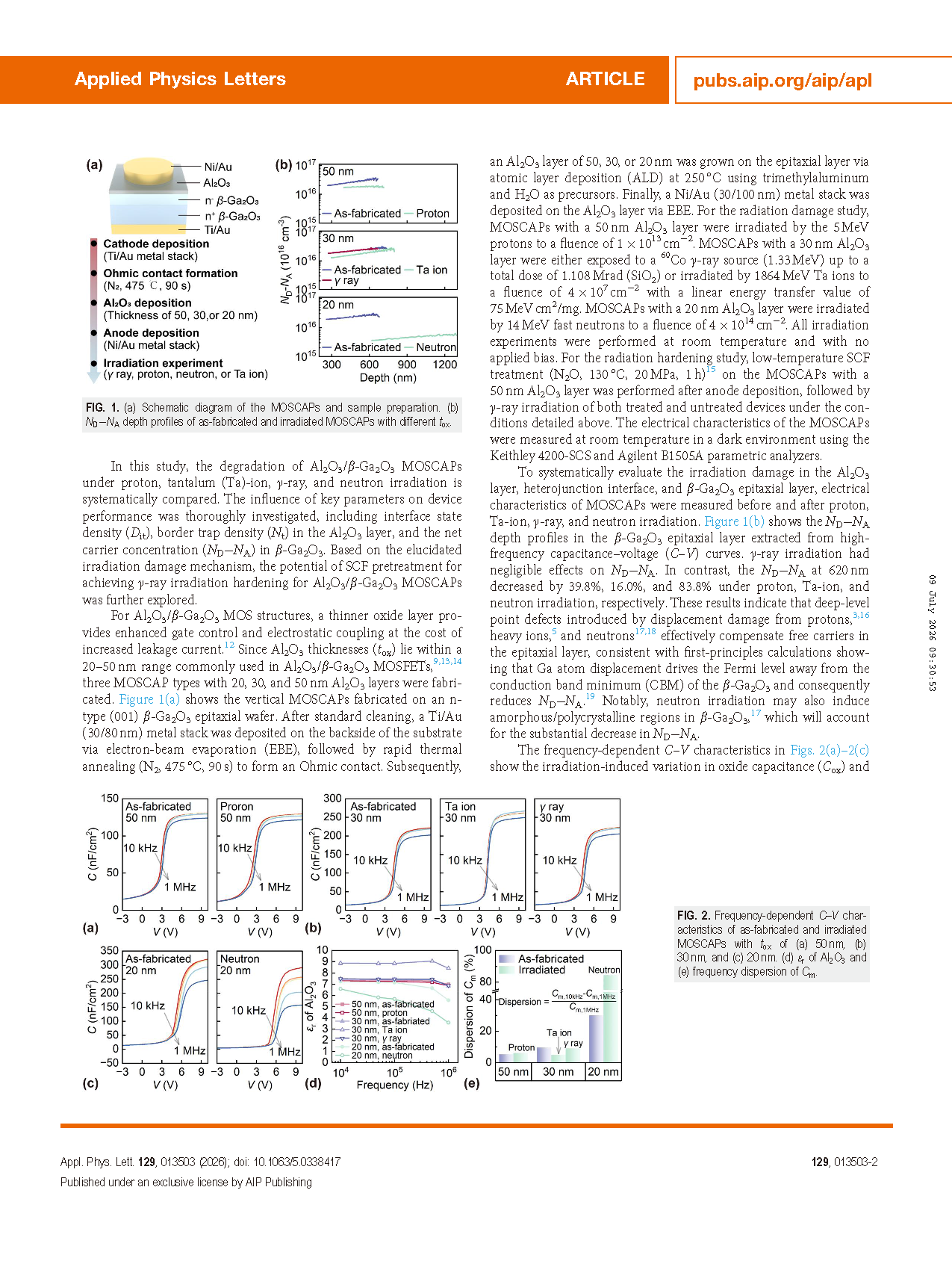
For Al₂O₃/β-Ga₂O₃ MOS structures, a thinner oxide layer provides enhanced gate control and electrostatic coupling at the cost of increased leakage current. Since Al₂O₃ thicknesses (tox) lie within a 20–50nm range commonly used in Al₂O₃/β-Ga₂O₃ MOSFETs, three MOSCAP types with 20, 30, and 50nm Al₂O₃ layers were fabricated. Figure 1(a) shows the vertical MOSCAPs fabricated on an n-type (001) β-Ga₂O₃ epitaxial wafer. After standard cleaning, a Ti/Au (30/80 nm) metal stack was deposited on the backside of the substrate via electron-beam evaporation (EBE), followed by rapid thermal annealing (N₂, 475 C, 90s) to form an Ohmic contact. Subsequently, an Al₂O₃ layer of 50, 30, or 20nm was grown on the epitaxial layer via atomic layer deposition (ALD) at 250 C using trimethylaluminum and H₂O as precursors. Finally, a Ni/Au (30/100nm) metal stack was deposited on the Al₂O₃ layer via EBE. For the radiation damage study, MOSCAPs with a 50 nm Al₂O₃ layer were irradiated by the 5 MeV protons to a fluence of 1 ×10¹³ cm⁻². MOSCAPs with a 30 nm Al₂O₃ layer were either exposed to a ⁶⁰Co γ-ray source (1.33 MeV) up to a total dose of 1.108 Mrad (SiO₂) or irradiated by 1864MeV Ta ions to a fluence of 4 ×10⁷ cm⁻² with a linear energy transfer value of 75 MeV cm²/mg. MOSCAPs with a 20 nm Al₂O₃ layer were irradiated by 14 MeV fast neutrons to a fluence of 4 ×10¹⁴ cm⁻². All irradiation experiments were performed at room temperature and with no applied bias. For the radiation hardening study, low-temperature SCF treatment (N₂O, 20 MPa, 1 h) on the MOSCAPs with a 50nm Al₂O₃ layer was performed after anode deposition, followed by γ-ray irradiation of both treated and untreated devices under the conditions detailed above. The electrical characteristics of the MOSCAPs were measured at room temperature in a dark environment using the Keithley 4200-SCS and Agilent B1505A parametric analyzers.
Highlights
Systematic comparative investigation of proton, Ta-ion, γ-ray and neutron irradiation damage behaviors on Al₂O₃/β-Ga₂O₃MOSCAPs, revealing the coupling and competition mechanism among ionization damage, displacement damage and localized annealing effect.
Quantitatively characterize the evolution of border traps, interface states, net carrier concentration, leakage current and breakdown electric field under four irradiation sources; two unique damage mitigation mechanisms (neutron-induced carrier removal, Ta-ion localized annealing) are clarified.
Propose low-temperature supercritical fluid (SCF) pretreatment as an effective γ-ray radiation hardening strategy for Al₂O₃/β-Ga₂O₃ MOSCAPs via passivating oxygen vacancies in Al₂O₃, reducing breakdown voltage degradation from 8.03% to 2.18%.
Trap-assisted tunneling (TAT) model is adopted to interpret leakage current variation, and band structure evolution is used to explain the shift of electron trap energy levels after different irradiations.
Conclusion
In summary, this study elucidated the irradiation damage mechanisms of Al₂O₃/β-Ga₂O₃ MOSCAPs under proton, Ta-ion, γ-ray, and neutron irradiation and further employed SCF pretreatment to achieve γ-ray radiation hardening. On the one hand, regarding the radiation damage mechanism: The decrease in Vfb,1 and the increase in ΔVfb after γ-ray irradiation originated from the conversion of hole-trapping centers into electron traps by capturing holes, which uncovered the ionization damage in the devices. Proton, Ta-ion, and neutron irradiation introduced additional displacement damage, directly leading to an increase in border traps and interface traps. Both damages contributed to increased leakage current and reduced Ebr. Notably, the reduction in frequency dispersion of Cm, ΔVfb, and Dit confirmed that the localized annealing effect induced by Ta-ion irradiation partly passivated the traps at the heterojunction, although the effect did not dominate the forward current characteristics. In contrast, the significant reduction in ND−NA caused by neutron irradiation effectively enhanced the Ebr. On the other hand, regarding the radiation hardening: Before γ-ray irradiation, SCF pretreatment passivated border traps and interface traps, improving overall device performance, including reduced leakage current and increased Vbr with improved uniformity. Furthermore, after γ-ray irradiation, the decreased concentration of Vₒ⁰ available to respond to ionization damage led to a lower Nt increase in SCF-treated MOSCAPs. Consequently, SCF pretreatment enhanced γ-ray irradiation resistance, as manifested by the suppression of irradiation-induced increase in leakage current and the reduction in Vbr degradation from 8.03% to 2.18%. This study provides insights into the irradiation damage mechanisms of Al₂O₃/β-Ga₂O₃ MOSCAPs and offers a reference for radiation-hardening design of similar MOS devices.
Project Support
This work was supported by the National Natural Science Foundation of China under Grant No. 12575199, the Steady Support Fund for National Key Laboratory under Grant No. JBSY252800260, the State Key Laboratory of Optoelectronic Materials and Technologies (Sun Yat-sen University) under Grant No. OEMT-2025-KF-03, and the Fundamental Research Funds for the Central Universities under Grant Nos. xtr052025030, xxj032025008, and xzy012024156.
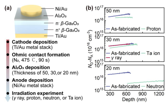
Fig. 1. (a) Schematic diagram of the MOSCAPs and sample preparation. (b) ND−NA depth profiles of as-fabricated and irradiated MOSCAPs with different tox.
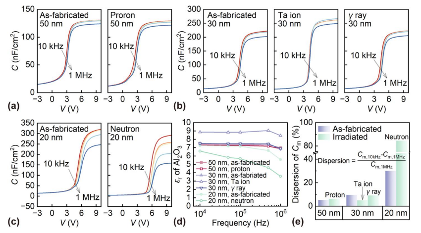
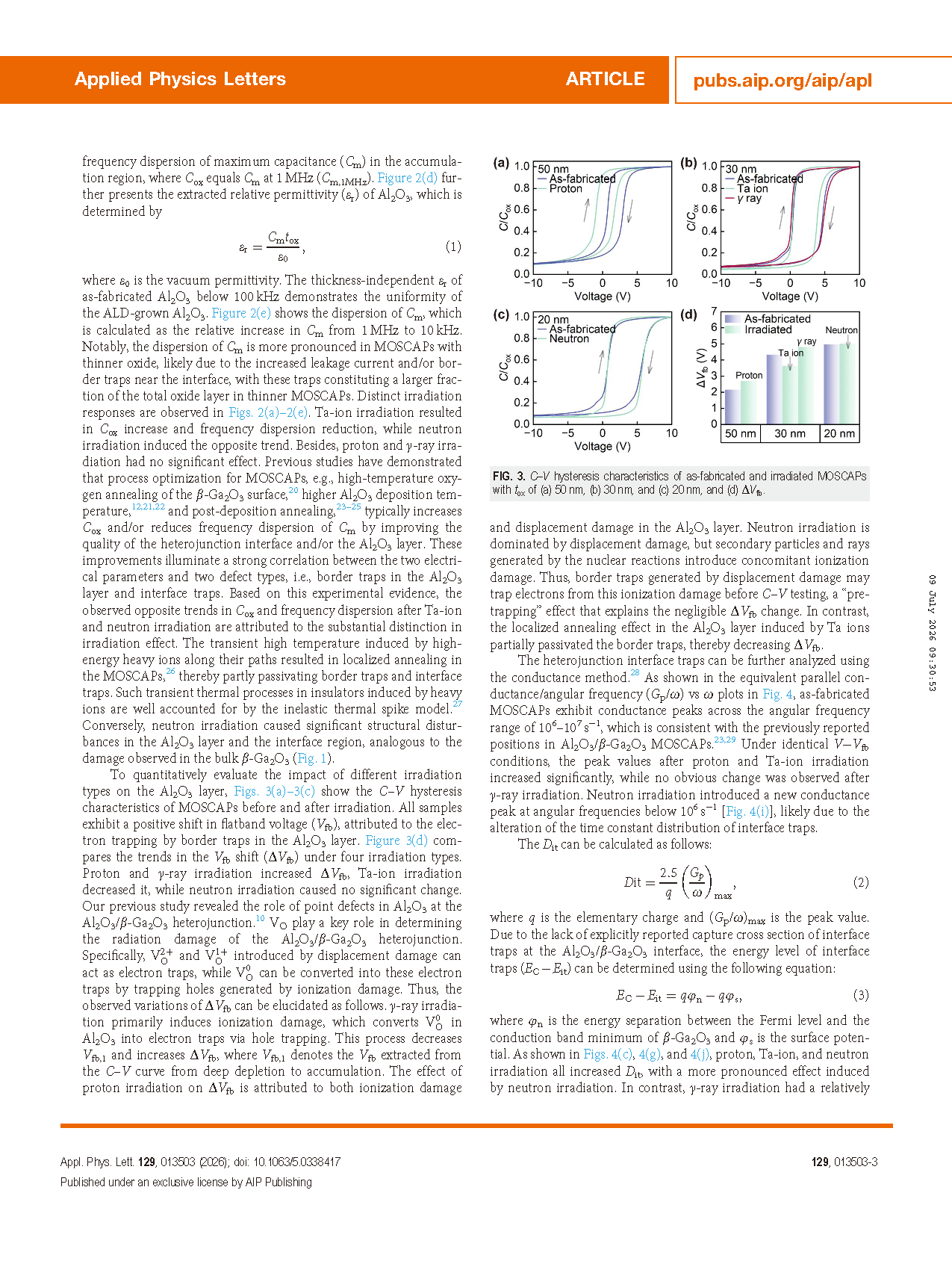
Fig. 2. Frequency-dependent C–V characteristics of as-fabricated and irradiated MOSCAPs with tox of (a) 50 nm, (b) 30nm, and (c) 20nm.(d) Relative permittivity εr of Al₂O₃ and (e) frequency dispersion of Cm.
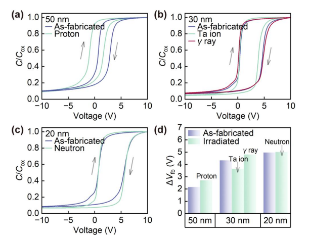
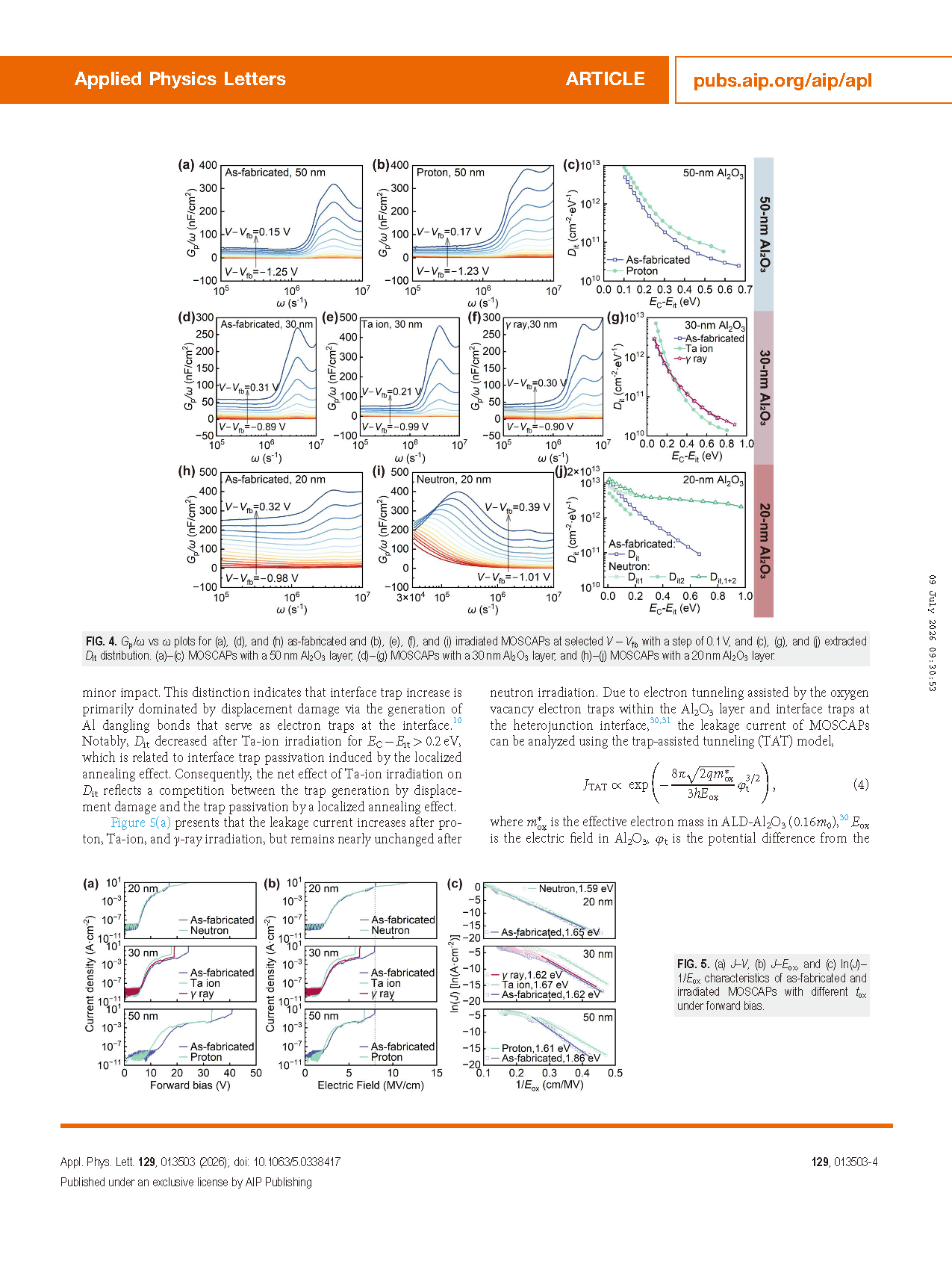
Fig. 3. C–V hysteresis characteristics of as-fabricated and irradiated MOSCAPs with tox of (a) 50 nm, (b) 30 nm, and (c) 20 nm, and (d) ΔVfb comparison under four irradiation types.
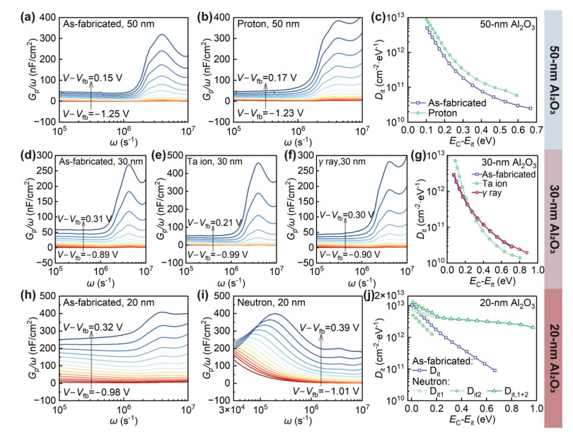
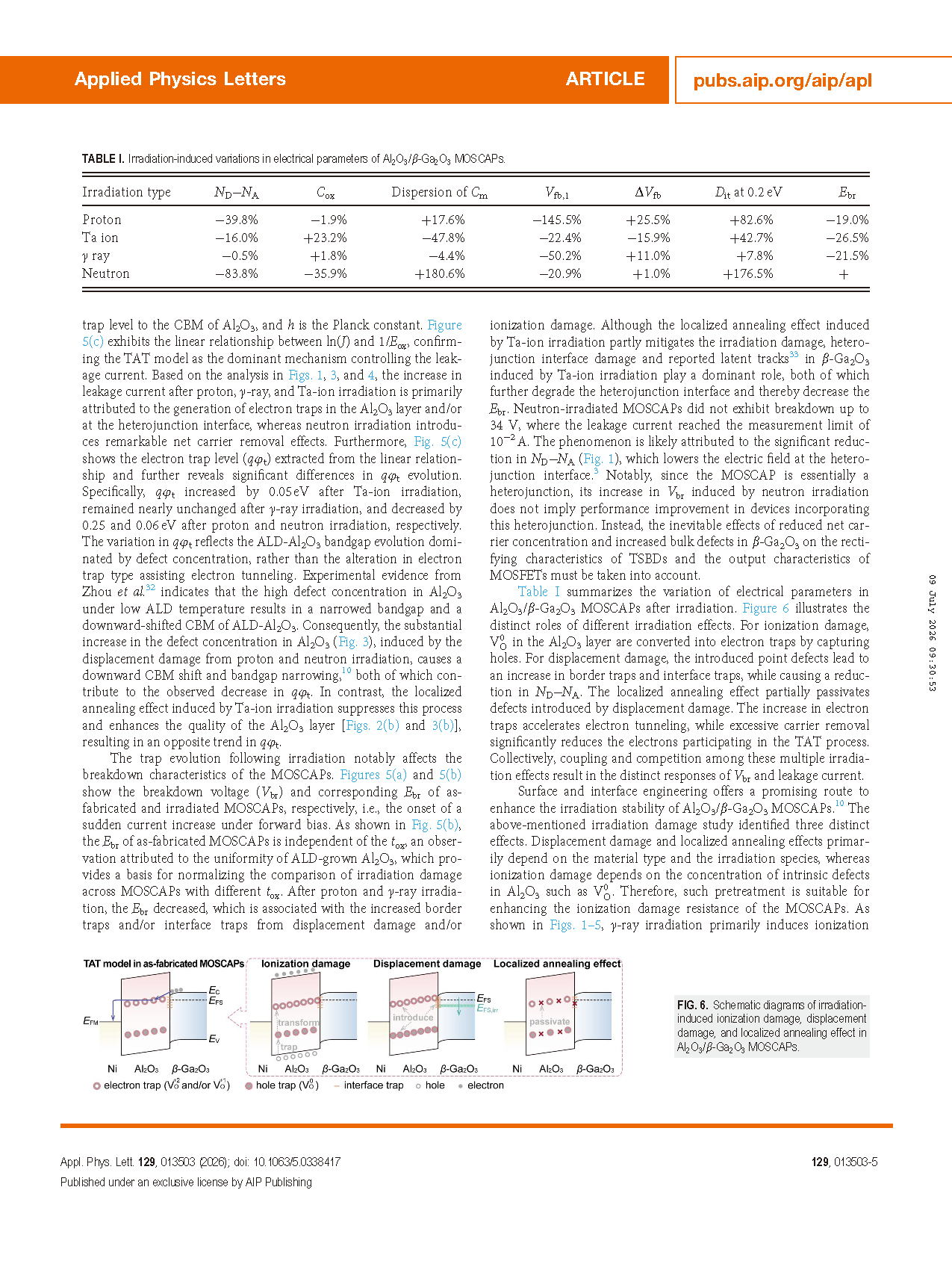
Fig. 4. Gp/ω vs ω plots for (a), (d), and (h) as-fabricated and (b), (e), (f), and (i) irradiated MOSCAPs at selected V−Vfb with a step of 0.1 V, and (c), (g), and (j) extracted Dit distribution. (a)–(c) MOSCAPs with a 50 nm Al₂O₃ layer; (d)–(g) MOSCAPs with a 30 nm Al₂O₃ layer; and (h)–(j) MOSCAPs with a 20 nm Al₂O₃ layer.
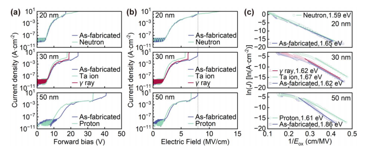
Fig. 5. (a) J–V, (b) J-E, and (c) ln (J)-1/Eox characteristics of as-fabricated and irradiated MOSCAPs with different tox under forward bias.
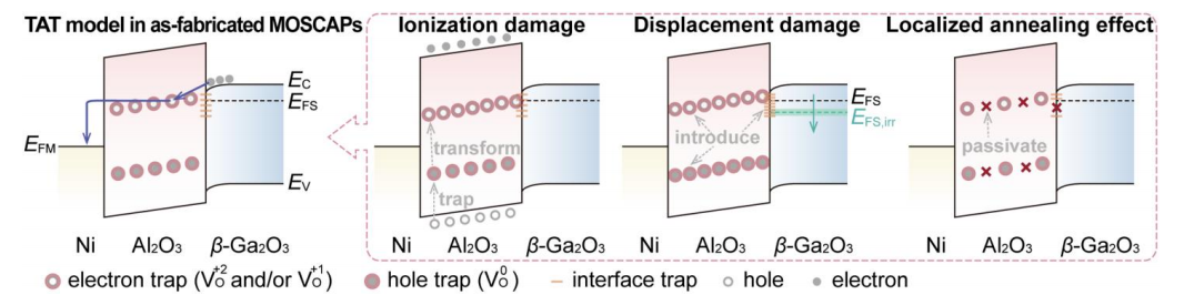
Fig. 6. Schematic diagrams of irradiation-induced ionization damage, displacement damage, and localized annealing effect in Al₂O₃/β-Ga₂O₃ MOSCAPs.
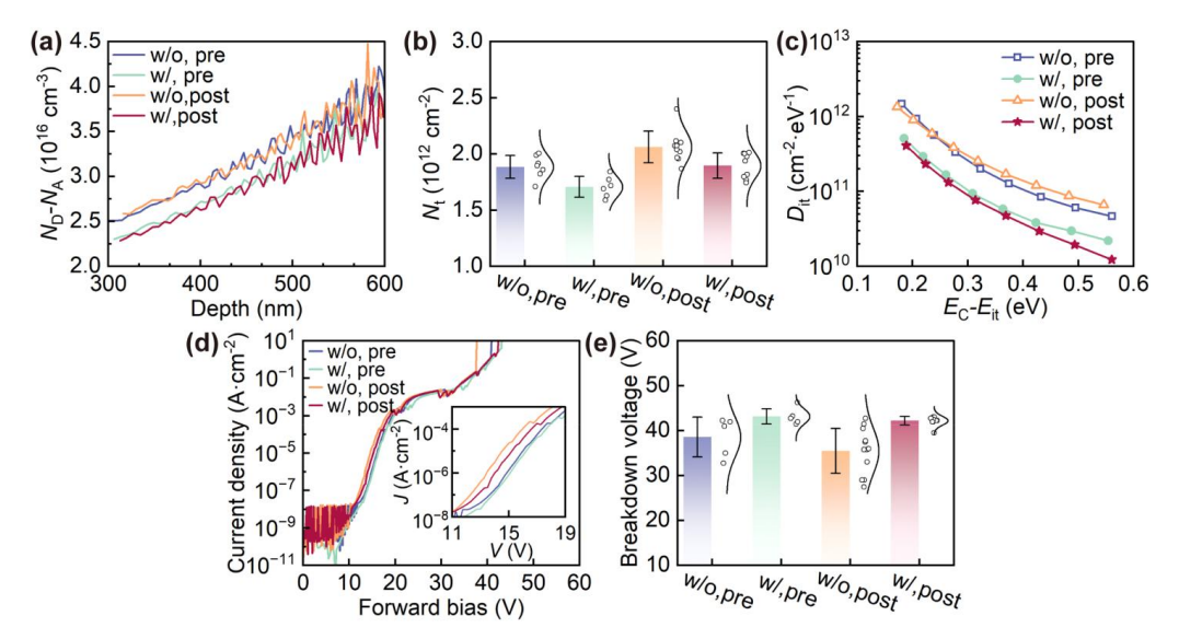
Fig. 7. Electrical characteristics of 50 nm Al₂O₃/β-Ga₂O₃ MOSCAPs with (w/) and without (w/o) SCF pretreatment, before (pre) and after (post) γ-ray irradiation. (a) ND−NA depth profiles, (b) Nt, (c) Dit, (d) J–V characteristics, and (e) statistics of breakdown voltage.
DOI :
10.1063/5.0338417
Instruction
Official Account

Cooperation
Top
