


Researchers from Southern University of Science and Technology and King Faisal University have published a paper titled "Geometry-Driven Performance Enhancement in h-BN / β-Ga₂O₃ Heterostructures for Solar-Blind and Polarization-Sensitive Photodetection" in ACS Applied Materials & Interfaces.
Background
Solar-blind ultraviolet photodetectors respond only to 200–280 nm light, which is fully absorbed by atmospheric ozone to eliminate solar background noise, making them vital for flame monitoring, ozone detection and environmental sensing. Traditional wide-bandgap materials like AlGaN and ZnMgO rely on costly epitaxial growth; heavy doping generates massive lattice defects and degrades detection sensitivity. β-Ga₂O₃ has an ultrawide intrinsic bandgap (~4.8 eV) for filter-free solar-blind detection with low-cost single-crystal substrates, yet pristine β-Ga₂O₃ suffers inefficient carrier collection and weak photoresponse. Hexagonal boron nitride (h-BN) is a 2D van der Waals insulator with dangling-bond-free surface, serving as an ideal interfacial passivation layer. Few works systematically compare lateral and vertical h-BN/β-Ga₂O₃ device architectures, and low-cost exfoliated heterostructures combining high responsivity and polarization sensitivity remain underexplored. In this work, mechanically exfoliated dry transfer is adopted to construct clean vdW interfaces. The optoelectronic and polarization performances of two geometries are systematically compared, and geometry-modulated carrier separation mechanism is clarified, offering a facile route toward high-performance solar-blind polarization photodetectors.
Abstract
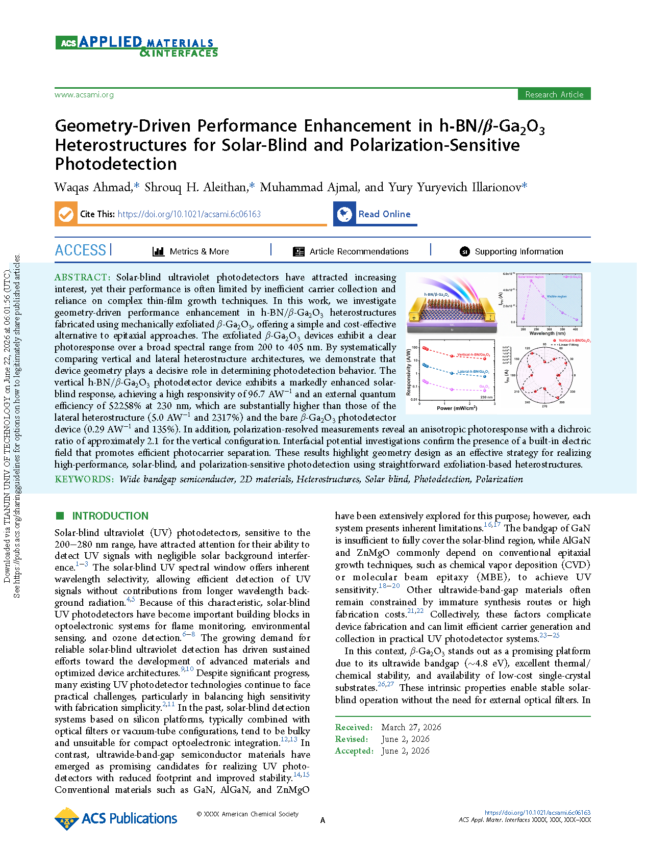
Solar-blind ultraviolet photodetectors have attracted increasing interest, yet their performance is often limited by inefficient carrier collection and reliance on complex thin-film growth techniques. In this work, we investigate geometry-driven performance enhancement in h-BN / β-Ga₂O₃ heterostructures fabricated using mechanically exfoliated β-Ga₂O₃, offering a simple and cost-effective alternative to epitaxial approaches. The exfoliated β-Ga₂O₃ photoresponse over a broad spectral range from 200 to 405 nm. By systematically comparing vertical and lateral heterostructure architectures, we demonstrate that device geometry plays a decisive role in determining photodetection behavior. The h-BN / β-Ga₂O₃ photodetector device exhibits a markedly enhanced solarblind response, achieving a high responsivity of 96.7 AW⁻¹ and an external quantum efficiency of 52258% at 230 nm, which are substantially higher than those of the lateral device (5.0 AW⁻¹ and 2317%) and the bare β-Ga₂O₃ photodetector (0.29 AW⁻¹ and 135%). In addition, polarization-resolved measurements reveal an anisotropic photoresponse with a dichroic ratio of approximately 2.1 for the vertical configuration. Interfacial potential investigations confirm the presence of a built-in electric field that promotes efficient photocarrier separation. These results highlight geometry design as an effective strategy for realizing high-performance, solar-blind, and polarization-sensitive photodetection using straightforward exfoliation-based heterostructures.
Highlights
Clean h-BN/β-Ga₂O₃van der Waals heterostructures are fabricated via mechanical exfoliation and dry transfer without epitaxy, greatly reducing fabrication difficulty and cost;
Lateral and vertical device geometries are systematically compared for the first time, verifying vertical architecture shortens carrier transport path and strengthens interfacial built-in electric field;
Vertical device achieves responsivity of 96.7 A/W and EQE of 52258% at 230 nm, 19 times higher than lateral device and 333 times higher than pristine β-Ga₂O₃with faster temporal response;
Vertical heterostructure realizes polarization-sensitive photodetection with a high dichroic ratio of 2.1, superior to lateral counterparts, expanding the application of Ga₂O₃devices in polarization imaging;
KPFM directly observes a 638 mV interfacial potential drop, fully illustrating the physical mechanism of band bending and built-in electric field accelerating photocarrier separation.
Conclusion
In summary, this work demonstrates that device architecture plays a pivotal role in determining the photodetection performance of h-BN / β-Ga₂O₃ heterostructures. The vertical configuration delivers a pronounced enhancement in solar-blind UV detection, achieving an R of 96.7 AW⁻¹ and an EQE of 52258% at 230 nm, which are markedly higher than those of the lateral device and the pristine β-Ga₂O₃ photodetector. Beyond photodetection performance, polarization-resolved measurements reveal a clear anisotropic photoresponse, with the vertical heterostructure exhibiting a dichroic ratio of approximately 2.1. Interfacial potential analysis confirms the presence of an internal electric field at the h-BN / β-Ga₂O₃ junction, which promotes efficient photocarrier separation and reduces recombination losses. Additionally, the vertical device shows a faster temporal response, with a rise time of ∼11 ms, compared with ∼19 ms for the lateral architecture and ∼55 ms for bare β-Ga₂O₃. Collectively, these findings highlight geometry-driven interface engineering as an effective and scalable strategy for realizing high-performance, solar-blind, and polarization-sensitive photodetectors using exfoliation-based heterostructures.
Project Support
This work was supported by the National Natural Science Foundation of China (NSFC) under grant number W2432040, the Guangdong Basic and Applied Basic Research Foundation (2023ZT10X010, 2024A1515010179), and Shenzhen Key Laboratory of Phononics and Intelligent Thermal Materials (SYSRD20250529114001002), Shenzhen 518055, P. R. China. This work was supported through the Annual Funding track by the Deanship of Scientific Research, Vice Presidency for Graduate Studies and Scientific Research, King Faisal University, Saudi Arabia, Project No. KFU260631.
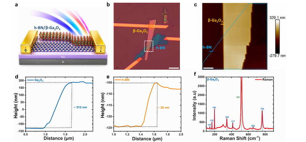
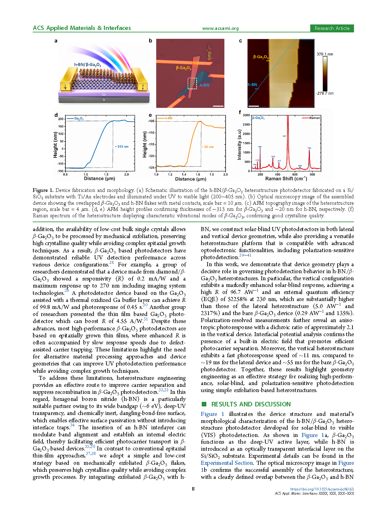
Figure 1 Device fabrication and morphology. (a) Schematic illustration of the h-BN/β-Ga₂O₃ heterostructure photodetector fabricated on a Si/SiO₂ substrate with Ti/Au electrodes and illuminated under UV to visible light (200 - 405 nm). (b) Optical microscopy image of the assembled device showing the overlapped β-Ga₂O₃ and h-BN flakes with metal contacts, scale bar = 10 μm. (c) AFM topography image of the heterostructure region, scale bar = 4 μm. (d, e) AFM height profiles confirming thicknesses of ~313 nm for β-Ga₂O₃ and ~20 nm for h-BN, respectively. (f) Raman spectrum of the heterostructure displaying characteristic vibrational modes of β-Ga₂O₃ confirming good crystalline quality.
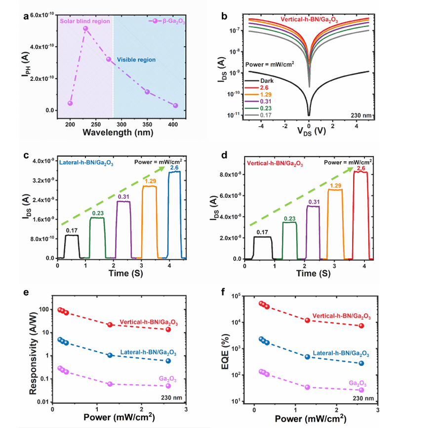
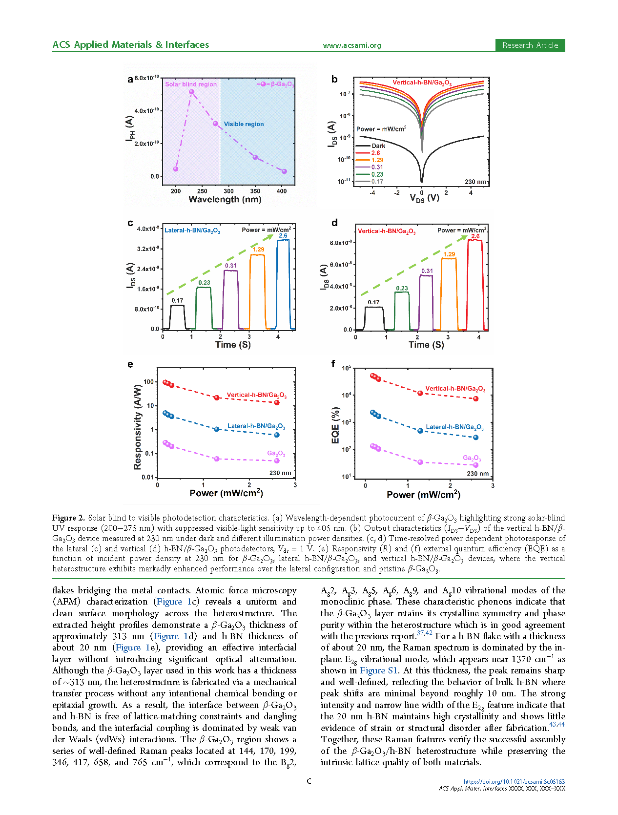
Figure 2 Solar blind to visible photodetection characteristics. (a) Wavelength-dependent photocurrent of β-Ga₂O₃ highlighting strong solar-blind UV response (200−275 nm) with suppressed visible-light sensitivity up to 405 nm. (b) Output characteristics (IDS-VDS) of the vertical h-BN/β-Ga₂O₃ photodetector, I-V curves of the lateral (c) and vertical (d) h-BN/β-Ga₂O₃ photodetectors, Vds=1 V as a function of incident power density at 230 nm for β-Ga₂O₃, lateral h-BN/β-Ga₂O₃, vertical h-BN/β-Ga₂O₃ devices, where the vertical heterostructure exhibits markedly enhanced performance over the lateral configuration and pristine β-Ga₂O₃. (e) Responsivity comparison, (f) EQE comparison of three devices.
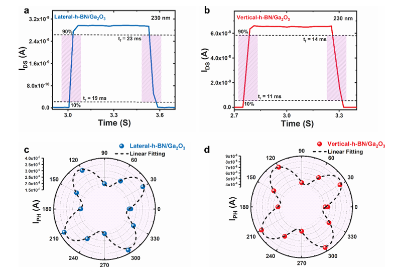
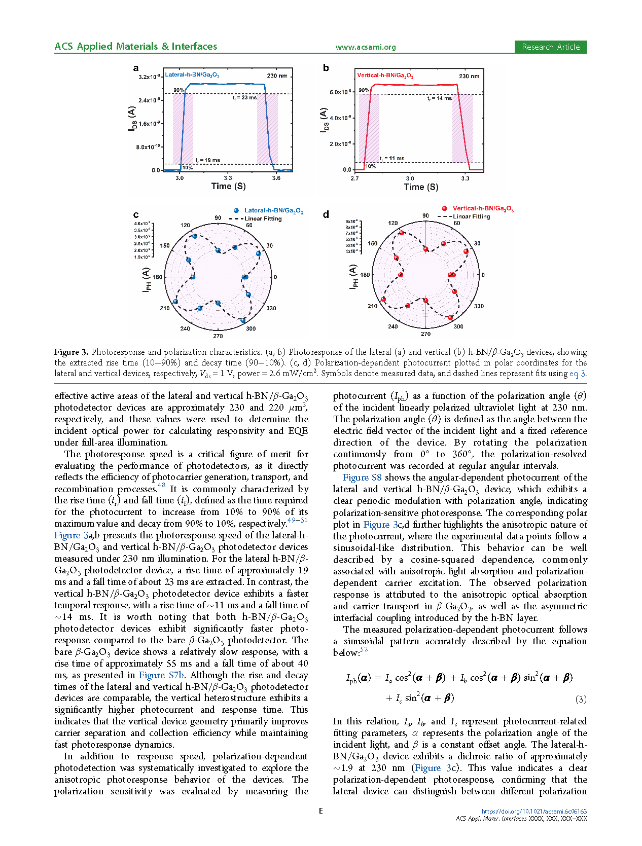
Figure 3 Photoresponse and polarization characteristics. (a, b) Photoresponse of the lateral (a) and vertical (b) h-BN / β-Ga₂O₃ devices, showing the extracted rise time (10−90%) and decay time (90−10%). (c, d) Polarization-dependent photocurrent plotted in polar coordinates for the lateral and vertical devices, respectively, Vds=1 V, power =2.6 mW/cm². Symbols denote measured data, and dashed lines represent fits using eq 3.
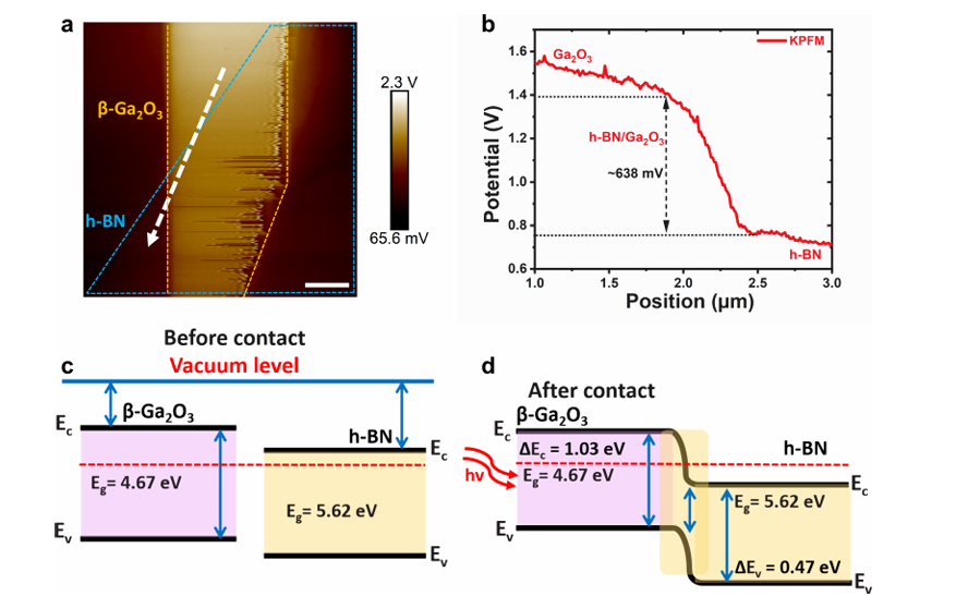
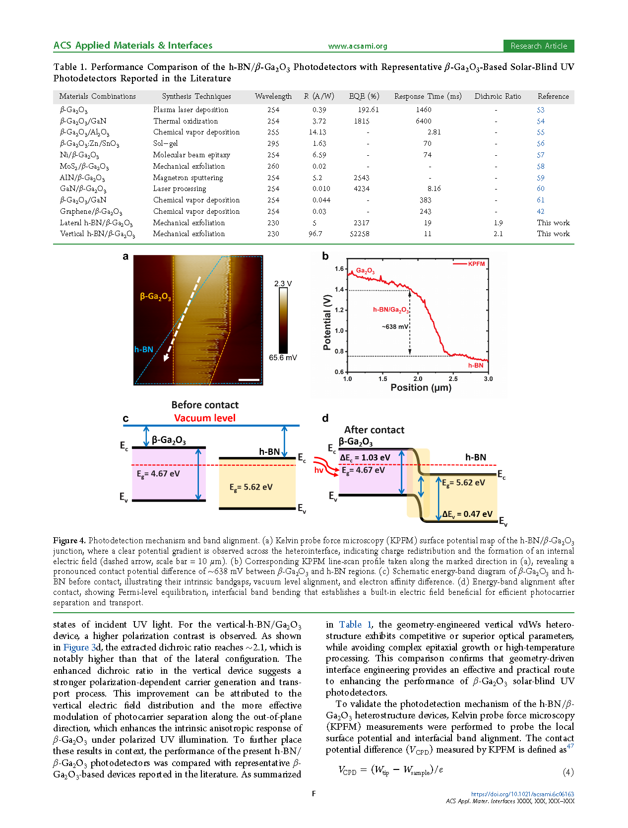
Figure 4 Photodetection mechanism and band alignment. (a) Kelvin probe force microscopy (KPFM) surface potential map of the h-BN / β-Ga₂O₃ junction, where a clear potential gradient is observed across the heterointerface, indicating charge redistribution and the formation of an internal electric field (dashed arrow, scale bar =10 μm). (b) Corresponding KPFM line-scan profile taken along the marked direction in (a), revealing a pronounced contact potential difference of ∼638 mV between β-Ga₂O₃ and h-BN regions. (c) Schematic energy-band diagram of β-Ga₂O₃ and h-BN before contact, illustrating their intrinsic bandgaps, vacuum level alignment, and electron affinity difference. (d) Energy-band alignment after contact, showing Fermi-level equilibration, interfacial band bending that establishes a built-in electric field beneficial for efficient photocarrier separation and transport.
DOI:
doi.org/10.1021/acsami.6c06163

Instruction
Official Account

Cooperation
Top
