


Introduction:
Within the Ga₂O₃ material system, high-quality single-crystal substrates provide the essential material foundation required for device fabrication. However, achieving high breakdown voltage, low conduction loss, and precisely controlled device structures cannot rely on substrates alone.
The epitaxial layer plays a critical role in constructing the functional regions of semiconductor devices. Through epitaxial growth, key parameters such as material thickness, carrier concentration, doping profiles, and multilayer structures can be precisely controlled, directly influencing current transport, electric-field distribution, and breakdown characteristics in devices. Particularly for high-voltage power devices, the drift layer typically requires high-quality epitaxial growth, and its crystal quality and electrical properties largely determine the performance limits of the final devices.
In other words, epitaxy is not simply a “regrowth” process after substrate preparation. Instead, it serves as a core technological bridge connecting single-crystal materials with high-performance devices, representing a crucial step in translating the material advantages of Ga₂O₃ into practical device applications.
In this issue, we will start from the fundamentals of epitaxial growth and further explore the importance of β-Ga₂O₃ epitaxy as well as its technological development.
Issue 9
Epitaxy Technology: A Key Bridge Connecting Ga₂O₃ Materials and Device Applications
What Is Epitaxy?
Epitaxy refers to the process of growing a crystalline layer on the surface of a crystal substrate, where the grown layer maintains a well-defined crystallographic orientation relationship with the underlying substrate. The resulting crystalline layer is known as an epitaxial layer.
(Reference: IUPAC Gold Book, “Epitaxy” entry)
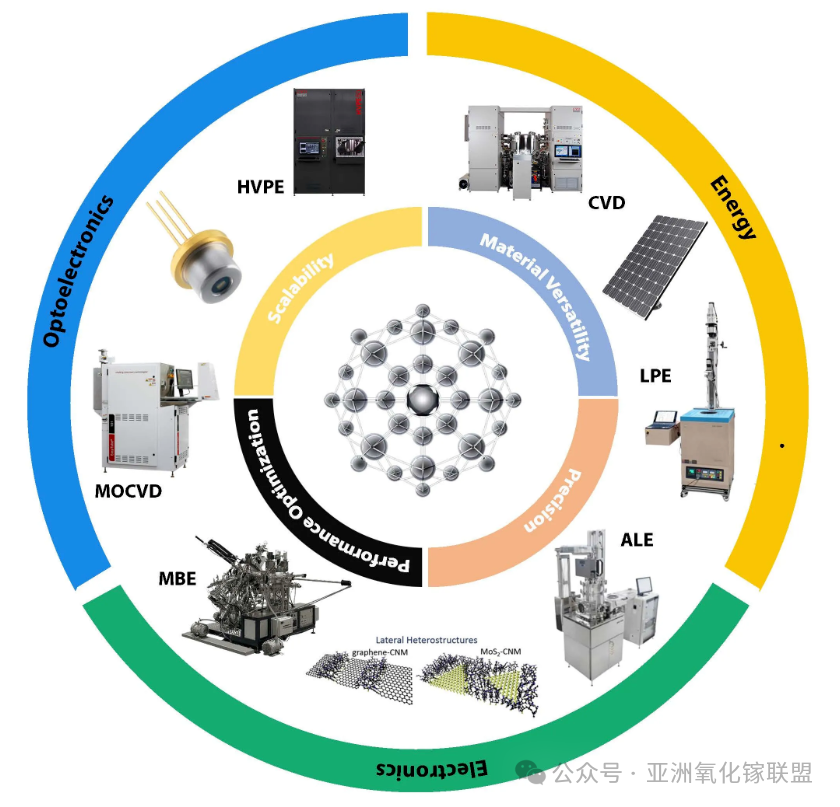
Fig. 1. Schematic illustration of semiconductor epitaxy technology systems and typical application areas [1]
The epitaxial layer is not simply deposited on the substrate surface; instead, it maintains a specific crystallographic orientation relationship with the underlying crystal substrate. The substrate not only provides mechanical support but also serves as a crystallographic template during epitaxial growth, playing a critical role in determining the nucleation and orientation of the grown layer.
Taking β-Ga₂O₃ as an example, the growth of β-Ga₂O₃ on a β-Ga₂O₃ single-crystal substrate is referred to as homoepitaxy. In contrast, the growth of Ga₂O₃ on substrates made of different materials, such as sapphire or SiC, is classified as heteroepitaxy.
Compared with heteroepitaxy, homoepitaxy avoids significant lattice and thermal expansion mismatches between different materials, making it more favorable for achieving high-quality single-crystal epitaxial layers. Therefore, it has become one of the key material approaches for developing high-performance β-Ga₂O₃ power devices.
Why Is Epitaxy Needed?
From a materials perspective, high-quality β-Ga₂O₃ single-crystal substrates already possess a well-defined crystal structure and can achieve different electrical properties through doping. So why is it still necessary to grow an additional epitaxial layer? The key reason is that the substrate and the device functional layer serve different roles and therefore have different requirements for material properties.
Taking a typical vertical power device as an example, the device needs to minimize resistance losses during current conduction in the on-state, while also withstanding high reverse voltage and electric fields in the off-state. To achieve both low on-resistance and high breakdown voltage, power devices generally adopt material structures with different doping levels.
A highly doped conductive substrate provides low electrical resistance, mechanical support, and an efficient low-resistance current path. In contrast, the drift region, which is responsible for sustaining most of the blocking voltage, typically requires a much lower net doping concentration and sufficient thickness. This enables the formation of a wider depletion region and allows the device to withstand higher reverse voltages.
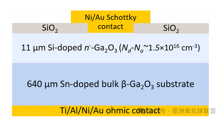
Fig. 2. Schematic cross-sectional structure of a vertical Ga₂O₃ SBD [2]
One of the key roles of epitaxial growth is to further construct functional layers that meet device requirements on high-quality substrates, enabling independent control over thickness, doping concentration, and material properties.
Thickness Control
The required thickness of the functional layer varies depending on the specific device application. For high-voltage power devices, the drift layer typically needs to be sufficiently thick to withstand high reverse voltages.
However, as the thickness increases, challenges associated with growth time, defect control, thickness uniformity, and surface morphology become increasingly significant. Achieving a balance between growth rate and material quality remains one of the key challenges in thick-film epitaxial growth.
Doping Control
Epitaxial growth also enables precise control over carrier concentration. By adjusting doping conditions during the growth process, material layers with different electrical properties can be obtained on the same substrate. This allows device structures to move beyond a single, uniform doping profile and enables targeted material design according to the functional requirements of different regions within the device.
Multilayer Structure Design
Furthermore, epitaxial growth enables the construction of multilayer structures by tailoring material composition or doping conditions. For example, layers with different doping concentrations can be engineered to form highly doped layers, lightly doped layers, and other functional layers. In addition, heterostructures can be constructed by integrating different materials, providing greater flexibility for band structure engineering, carrier confinement, and advanced device architecture design.
Ga₂O₃ Epitaxy Technology Routes
At present, Ga₂O₃ epitaxy has evolved into a variety of technological approaches, each with distinct characteristics in terms of precursor supply, transport mechanisms, and surface reaction processes. Based on the generation and transport methods of growth species, as well as the film formation process, these techniques can be broadly classified into two categories: chemical vapor deposition (CVD) and physical vapor deposition (PVD).
CVD-based methods mainly use gallium-containing precursors and oxygen sources as growth species. Through gas-phase transport, aerosol-assisted transport, or volatile halide intermediate transport, the growth species are delivered to the vicinity of the substrate, where precursor decomposition, oxidation reactions, and surface chemical reactions occur, ultimately forming Ga₂O₃ epitaxial layers. Representative techniques include metal-organic chemical vapor deposition (MOCVD), mist chemical vapor deposition (Mist-CVD), and halide vapor phase epitaxy (HVPE).
In contrast, PVD-based methods generate and transport growth species primarily through physical processes. Representative techniques mainly include pulsed laser deposition (PLD) and molecular beam epitaxy (MBE).
MOCVD
Metal-organic chemical vapor deposition (MOCVD) is one of the key epitaxial growth techniques for Ga₂O₃. Its basic principle involves transporting metal-organic gallium precursors and oxygen sources to the vicinity of a heated substrate, where precursor decomposition and surface chemical reactions occur to form the Ga₂O₃ epitaxial layer. Common gallium precursors include trimethylgallium (TMGa) and triethylgallium (TEGa), while oxygen sources such as O₂ and H₂O can be used.
MOCVD features flexible process parameter control and strong doping modulation capability. It can be applied for high-quality Ga₂O₃ homoepitaxy and the preparation of device-grade epitaxial materials, making it one of the important techniques in current Ga₂O₃ epitaxial research.
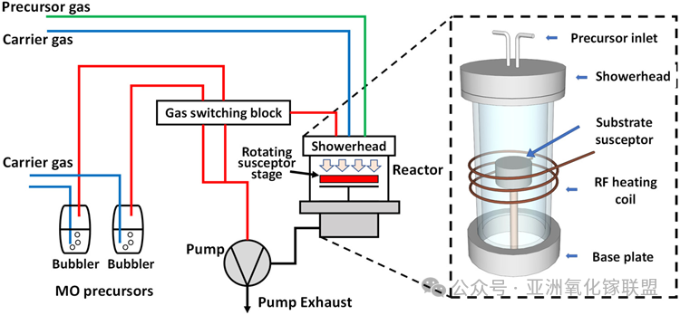
Fig. 3. Schematic illustration of a typical MOCVD reactor structure [3]
HVPE
Halide vapor phase epitaxy (HVPE) is an epitaxial growth technique that utilizes volatile gallium halides for gas-phase transport. During a typical growth process, gaseous species such as GaCl are transported to the high-temperature substrate region, where they react with oxygen sources to form a Ga₂O₃ epitaxial layer.
The most prominent advantages of HVPE are its high growth rate and strong capability for thick-film growth. Therefore, it is particularly suitable for fabricating thick drift layers required for high-voltage power devices, making it one of the key technologies for β-Ga₂O₃ thick-film epitaxy.
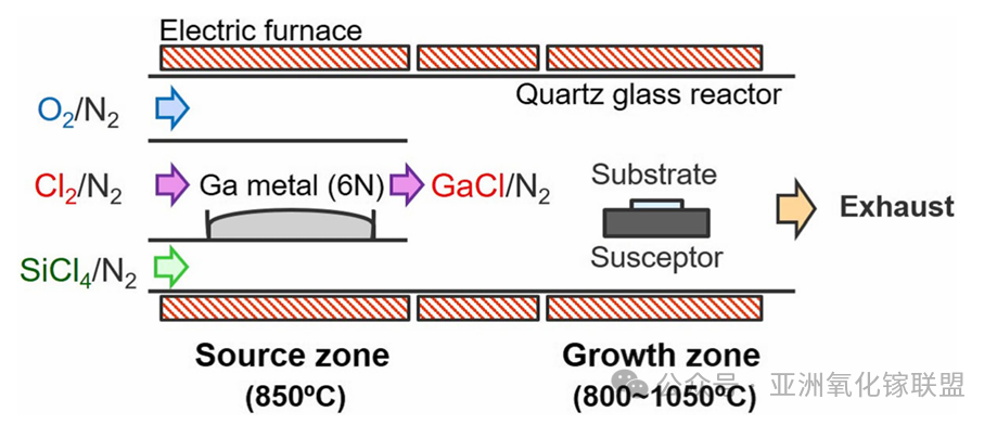
Fig. 4. Schematic diagram of an HVPE epitaxial growth system [4]
Mist-CVD
Mist chemical vapor deposition (Mist-CVD) is an epitaxial growth technique that converts a gallium-containing precursor solution into fine droplets or aerosols, which are then transported by a carrier gas to a heated substrate region. Through evaporation, precursor decomposition, and surface chemical reactions, Ga₂O₃ thin films or epitaxial layers are subsequently formed.
Mist-CVD features a relatively simple equipment structure, flexible precursor selection, and potential for low-cost fabrication. Currently, it is mainly applied in the study of α-Ga₂O₃ heteroepitaxial growth and large-area oxide thin-film deposition.
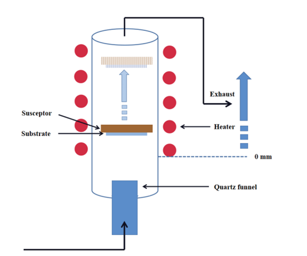
Fig. 5. Schematic illustration of a typical Mist-CVD reactor structure [5]
PLD
Pulsed laser deposition (PLD) is a widely used technique for the fabrication of oxide thin films. Its basic principle involves irradiating a target material with high-energy pulsed laser beams, causing instantaneous ablation of the target surface and generating a high-energy plume consisting of atoms, ions, and clusters. These energetic species are subsequently transported to the substrate surface, where they nucleate and grow into thin films.
PLD offers high process flexibility, allowing convenient adjustment of parameters such as substrate temperature, oxygen partial pressure, deposition flux, and kinetic energy of incident species. These factors enable precise control over nucleation and growth dynamics, making PLD suitable for investigating different crystal phases, substrate effects, and heteroepitaxial growth mechanisms. However, limitations remain in terms of large-area uniformity, particle control, and scalability, and therefore PLD is currently more commonly used for laboratory-scale material research.
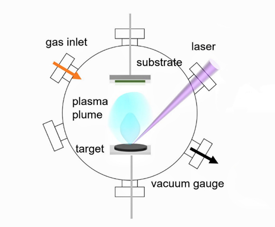
Fig. 6. Schematic illustration of a typical PLD system [6]
MBE
Molecular beam epitaxy (MBE) is an epitaxial growth technique featuring precise control over material deposition. It is typically performed under ultra-high vacuum conditions, where high-purity source materials generate directional atomic or molecular beams that are transported to a heated substrate surface. The growth species undergo adsorption, surface diffusion, and chemical reactions, ultimately forming an epitaxial layer.
The key advantage of MBE lies in its independently controllable beam fluxes and excellent capability for interface and thickness engineering, making it particularly suitable for the growth of ultrathin layers, heterostructures, and fundamental studies of growth mechanisms. In the field of gallium oxide, MBE has been widely employed for the epitaxial growth of β-Ga₂O₃ and related heterostructures.
However, MBE also faces limitations, including complex equipment requirements, stringent vacuum conditions, and relatively low growth rates under conventional growth modes. Therefore, its application remains relatively limited for thick-film growth and large-scale manufacturing.
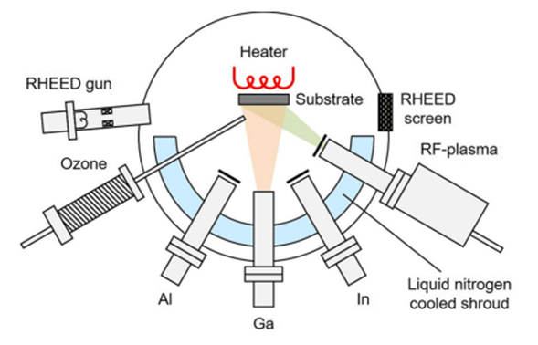
Fig. 7. Schematic illustration of an oxide MBE system [4]
Different epitaxial techniques exhibit distinct advantages in terms of growth rate, material quality, doping control, interface engineering, and scalability, leading to their suitability for different application scenarios. There is no simple hierarchy of superiority among these epitaxial methods. For Ga₂O₃, the selection of an appropriate epitaxial technique ultimately depends on the specific requirements of the target material and device, including thickness, doping concentration, crystal quality, interface structure, and manufacturing efficiency.
Summary of This Issue
From substrates to epitaxial layers, Ga₂O₃ material fabrication is becoming increasingly oriented toward device requirements. Whether based on PVD or CVD approaches, the core objective of epitaxial growth lies in precisely controlling the supply, transport, and surface reactions of growth species, thereby enabling the formation of epitaxial layers with specific crystal structures and material properties on suitable substrates.
Different epitaxial technologies emphasize different strengths: some focus on achieving high crystal quality and precise doping control, some are optimized for high-rate thick-film growth, while others are more suitable for interface engineering, phase regulation, and the exploration of emerging material systems. Therefore, the future development of Ga₂O₃ epitaxy does not depend on identifying a single “universal” process to replace all others. Instead, it requires the establishment of a complementary technology framework in which different approaches are selected according to specific material structures and device application requirements.
At present, key challenges for Ga₂O₃ epitaxial technology remain in simultaneously improving crystal quality and reducing defect density, while achieving precise control over doping concentration, epitaxial thickness, and material properties. In addition, further enhancement of wafer-scale uniformity, including both within-wafer and wafer-to-wafer consistency for large-size substrates, remains a critical direction for future technological advancement.
Inference:
[1] Intell. Sustain. Manuf. 2025, 2(1): 10011.
[2] IEEE Trans. Power Electron. 2021, 36(1): 41–44.
[3] J. Appl. Phys. 2023, 133(21): 211103.
[4] AAPPS Bull. 2022, 32: 3.
[5] J. Semicond. 2023, 44(6): 062803.
[6] J. Mater. Res. 2022, 37(1): 124–135.
Instruction
Official Account

Cooperation
Top
