


Ultra-wide-bandgap semiconductor gallium oxide (Ga₂O₃) has attracted extensive attention in recent years due to its combination of high critical breakdown field, high saturation electron drift velocity, intrinsic solar-blind ultraviolet response, and the capability of low-cost large-area single-crystal substrate fabrication through melt-based growth methods. It shows great potential in power and RF electronics, deep-ultraviolet detection, piezoelectric and ferroelectric devices, and intelligent sensing applications. The national “15th Five-Year Plan” outline has further emphasized the strategic importance of Ga₂O₃ by proposing to accelerate the industrialization of ultra-wide-bandgap semiconductors such as gallium oxide and diamond.
Vertical power devices, which utilize a vertical drift layer to sustain high voltages while improving current-carrying capability per unit chip area, are regarded as key device architectures for fully exploiting the advantages of Ga₂O₃ materials. Recently, the Nanofabrication Platform of Suzhou Institute of Nano-Tech and Nano-Bionics (SINANO), Chinese Academy of Sciences, in collaboration with the University of Science and Technology of China, Nanjing University, Henan Normal University, and University of Electronic Science and Technology of China, has achieved a series of advances in vertical Ga₂O₃ power devices.
The research has focused on various vertical device structures, including vertical fin field-effect transistors (FinFETs), current aperture vertical electron transistors (CAVETs), trench-gate metal-oxide-semiconductor field-effect transistors (UMOSFETs), and Schottky barrier diodes (SBDs). A range of advanced fabrication technologies has been developed, including localized bottom dielectric field modulation, all-ion-implantation planar processes, MOCVD sidewall regrowth, HF-based sidewall wet etching treatment, buried field plates, and composite edge termination structures.
The related achievements have been reported at the 2026 IEEE 38th International Symposium on Power Semiconductor Devices and ICs (ISPSD) and published in journals including Applied Physics Letters.
01 Localized Bottom Dielectric Field Modulation Enhances Breakdown Voltage of Vertical FinFETs (Paper 1)
Vertical Ga₂O₃ FinFETs can achieve normally-off operation without relying on p-type doping by utilizing the sidewall depletion effect of submicron fin channels. They also offer advantages including strong gate controllability, high cell density, and short current conduction paths, making them promising candidates for vertical power devices with high current density and low conduction losses. However, electric-field crowding tends to occur at the bottom corners of the fins, leading to premature breakdown.
Based on a controllable submicron-scale fin-shaped Ga₂O₃ etching technology, combined with photoresist planarization and self-aligned fabrication processes, the research team successfully fabricated enhancement-mode vertical FinFETs. To address electric-field concentration at the fin bottom and trench corners, a 100 nm-thick localized SiO₂ dielectric layer was further introduced to construct an internal electric-field modulation structure. This design effectively reduced the peak electric field at the fin bottom and improved the reverse blocking capability of the device.
With this localized dielectric modulation strategy, the breakdown voltage of the device was increased from 965 V to 1440 V. The device achieved a threshold voltage of 1.31 V, an on/off current ratio of approximately 10⁹, a transfer hysteresis of only 15 mV, a maximum output current density of 519.4 A/cm², a specific on-resistance of 12 mΩ·cm², and a figure of merit (FOM) of 137 MW/cm².
This work demonstrates that localized dielectric field modulation can significantly enhance the reverse blocking capability of vertical Ga₂O₃ FinFETs while maintaining excellent conduction performance, providing an effective strategy for the development of high-performance vertical Ga₂O₃ power devices. (Paper 1)
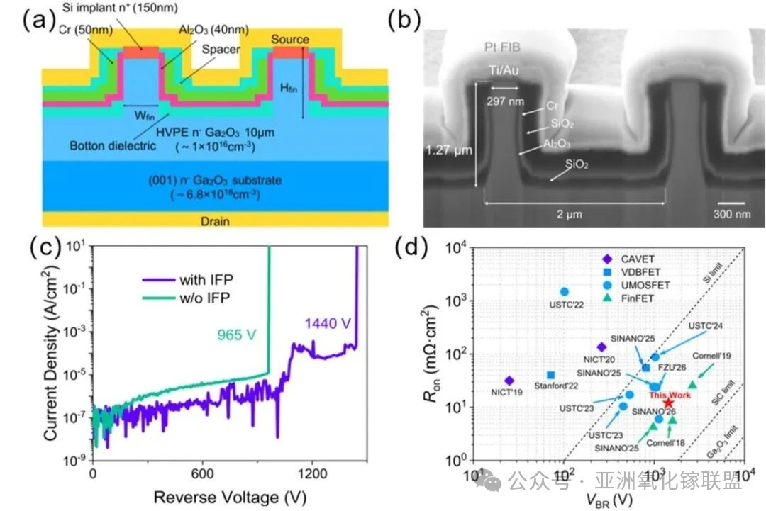
Fig. 1. (a) Schematic illustration of the bottom-dielectric multi-fin vertical β-Ga₂O₃ FinFET; (b) cross-sectional scanning electron microscopy (SEM) image of a representative device, with a designed fin width of 300 nm; (c) measured off-state breakdown characteristics of the vertical β-Ga₂O₃ FinFET; (d) benchmark comparison of the device performance and the relationship between specific on-resistance and breakdown voltage for β-Ga₂O₃ vertical MOSFETs.
02 All-Ion-Implantation Process Enables High-Voltage Planar-Gate CAVET (Paper 2)
Conventional vertical Ga₂O₃ devices typically rely on plasma etching to form trenches, mesas, or isolation regions. However, etching-induced damage can introduce interface defects and leakage paths, degrading threshold voltage stability and voltage blocking capability.
Leveraging the high-energy ion implantation equipment of the nanofabrication platform, the research team developed a planar-gate Ga₂O₃ CAVET featuring an all-ion-implantation process without mesa etching. The device employs multi-energy nitrogen ion implantation to form a graded current-blocking layer (CBL) with a depth of approximately 950 nm, silicon ion implantation to define the channel and source regions, and boron ion implantation for device isolation.
The fabricated CAVET achieved a positive threshold voltage of 3.4 V and a threshold voltage hysteresis of 116 mV. It delivered a maximum output current density of 714 A/cm², a specific on-resistance of 9.12 mΩ·cm², and a breakdown voltage of 1.36 kV.
This work demonstrates the effectiveness of graded nitrogen ion implantation in suppressing off-state leakage and enhancing voltage blocking capability. It also provides a new technological pathway for reducing etching-induced damage and improving the manufacturability of Ga₂O₃ power devices.
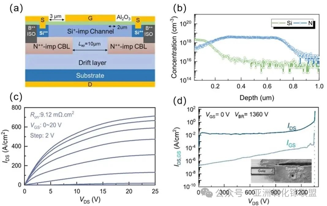
Fig. 2. (a) Cross-sectional schematic of the all-ion-implantation vertical β-Ga₂O₃ CAVET; (b) SIMS depth profiles of Si channel and N current-blocking layer (CBL) concentrations; (c) DC output characteristics of the device measured with gate voltage (VGS) swept from 0 to 20 V; (d) Off-state breakdown characteristics of the Ga₂O₃ CAVET measured at VGS= 0 V, with the inset showing a scanning electron microscopy image of the device failure location.
03 MOCVD Sidewall Regrowth for Improving UMOSFET On-State Performance (Papers 3 and 4)
β-Ga₂O₃ UMOSFETs offer advantages including high cell density, strong gate control capability, low input capacitance, and good process scalability, making them promising candidates for vertical power devices with high current density and low conduction losses. However, since the conductive channel is formed along the trench sidewalls, it is susceptible to the combined effects of plasma etching damage and nitrogen ion implantation compensation, which can reduce carrier concentration and mobility in the channel and ultimately limit device conduction performance.
Based on a self-modified oxide MOCVD system developed by the Nanofabrication Platform, the research team employed high-quality homoepitaxial growth technology to deposit an unintentionally doped Ga₂O₃ regrowth layer on the etched trench sidewalls. This approach shifts the conductive channel away from the original etched surface, where defect density is relatively high. Electrical measurements and Kelvin probe force microscopy (KPFM) results demonstrate that sidewall regrowth significantly enhances channel carrier concentration and electrical conductivity.
With 30 nm and 50 nm regrown layers, the devices achieved maximum output current densities of 359 A/cm² and 901 A/cm², respectively. Meanwhile, the specific on-resistance was reduced from 543.5 mΩ·cm² (without regrowth) to 11.8 mΩ·cm² and 7.9 mΩ·cm², respectively. Among them, the device with a 30 nm regrown layer achieved a power figure of merit (PFOM) of 42.5 MW/cm², representing more than an order-of-magnitude improvement compared with the device without sidewall regrowth.
This work demonstrates the effectiveness of sidewall regrowth in improving carrier transport in β-Ga₂O₃ trench channels and provides a pathway for future optimization of the trade-off between device conduction performance and breakdown capability through precise control of regrowth layer thickness and carrier concentration.
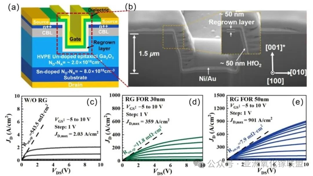
Fig. 3. (a) Schematic illustration of the β-Ga₂O₃ UMOSFET structure. (b) Cross-sectional scanning electron microscopy image of the β-Ga₂O₃ UMOSFET. DC output characteristics of β-Ga₂O₃ UMOSFETs with (c) no regrown layer, (d) a 30 nm regrown layer, and (e) a 50 nm regrown layer.
04 HF Sidewall Treatment of Ga₂O₃ UMOSFETs Enabling High Power Figure of Merit (Paper 5)
The trench sidewalls of Ga₂O₃ UMOSFETs are simultaneously affected by plasma etching damage and high-dose nitrogen implantation compensation. Deep-level defects can capture free electrons, increase channel resistance, and limit the device’s conduction capability.
To address these issues, the research team introduced an HF solution-based sidewall treatment prior to gate dielectric deposition. This process partially repairs etching-induced damage, reduces surface oxygen vacancies and interface traps, and locally incorporates fluorine into the near-surface region of the trench sidewalls. The shallow donor effect of fluorine increases the electron concentration in the sidewall channel and mitigates carrier compensation caused by nitrogen-related deep acceptor defects.
After HF treatment, the specific on-resistance was reduced from 91.7 mΩ·cm² to 6.0 mΩ·cm², while maintaining a breakdown voltage of 1132 V, resulting in a power figure of merit (PFOM) of 214 MW/cm². This work provides a low-cost and process-efficient surface engineering approach for simultaneously achieving high breakdown voltage and low conduction loss in Ga₂O₃ trench transistors.
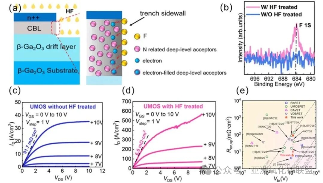
Fig. 4. (a) Schematic illustration of the HF treatment mechanism on the trench sidewalls of the β-Ga₂O₃ UMOSFET. (b) F 1s XPS spectra of β-Ga₂O₃ films after different treatments. DC output characteristics of β-Ga₂O₃ UMOSFETs with (c) no HF sidewall treatment and (d) HF sidewall treatment. (e) Benchmark plot of breakdown voltage (Vbr) versus specific on-resistance (RON,sp) for state-of-the-art vertical β-Ga₂O₃ MOSFETs reported to date.
05 Buried Field Shield Structure Enhances Breakdown Voltage of Ga₂O₃ UMOSFETs (Paper 6)
The bottom corners of vertical trench power devices are prone to localized electric-field crowding, which represents a critical limitation for the reverse blocking capability of Ga₂O₃ UMOSFETs.
Leveraging the platform’s high-energy ion implantation equipment, the research team proposed a selective multi-energy nitrogen ion implantation process at the bottom of the trench to form an approximately 300 nm-thick buried field shield layer. The highly resistive implanted region effectively redistributes the electric field at the trench bottom and suppresses electric-field concentration at the corners.
With the implementation of the buried field shield structure, the device breakdown voltage increased from 933 V to 1532 V, representing an improvement of approximately 600 V. Under a reverse bias of 1200 V, the peak electric field at the trench corner was reduced from 8.57 MV/cm to 6.43 MV/cm.
Currently, the lateral straggle of nitrogen implantation may still enhance carrier compensation in the sidewall channel. Further optimization of the implantation window, energy, and dose is required to achieve a better trade-off between breakdown capability and conduction performance. This work provides a new approach for internal electric-field management in kilovolt-class Ga₂O₃ trench transistors.
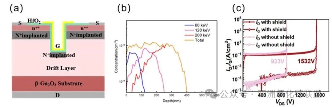
Fig. 5. (a) Schematic illustration of the β-Ga₂O₃ UMOSFET with an N-ion implantation-based field shield structure. (b) SIMS-simulated N-ion implantation profile and parameters at the trench bottom. (c) Breakdown characteristics of the β-Ga₂O₃ UMOSFET.
06 Composite Termination Structure Enables High-Voltage Vertical Ga₂O₃ Schottky Barrier Diodes (Paper 7)
Vertical Ga₂O₃ Schottky barrier diodes (SBDs) offer advantages including low forward voltage and unipolar conduction characteristics. However, electric-field crowding at the edge of the Schottky contact can lead to increased surface leakage current and premature breakdown, limiting device performance.
Based on the platform’s ion implantation equipment and etching technologies, the research team developed a composite termination structure consisting of an N-ion implantation guard ring, trench field-limiting ring, and floating metal rings. The N-ion implanted region forms a high-resistance zone around the anode, while the trench field-limiting ring and floating metal rings further redistribute the edge electric field in the termination region.
The breakdown voltage of the device without termination was only 91 V. After introducing a single N-ion implantation termination, the breakdown voltage increased to 1019 V, and with the composite termination structure, it was further enhanced to 1768 V. The composite-terminated device simultaneously achieved a low forward voltage of approximately 0.697 V, a specific on-resistance of 5.72 mΩ·cm², and a power figure of merit (PFOM) of 0.55 GW/cm².
Under a reverse bias of 1000 V, the composite termination reduced the peak electric field of the device from 6.27 MV/cm to 4.23 MV/cm and significantly improved the electric-field distribution near the floating metal rings.
This work provides a new termination design strategy for achieving high-voltage, low-loss vertical Ga₂O₃ rectifier devices.
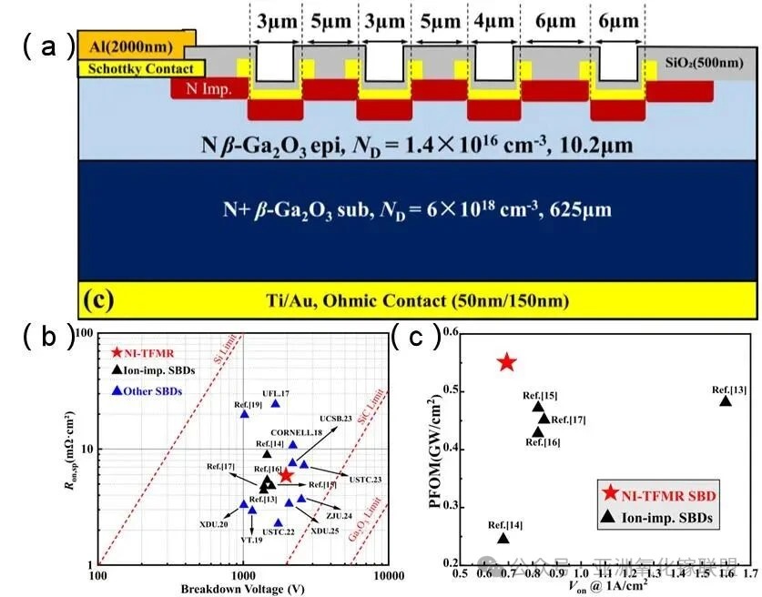
Fig. 6. (a) Schematic illustration of the vertical β-Ga₂O₃ SBD with an N-ion implantation guard ring, trench field-limiting ring, and floating metal ring (NI-TFMR) termination structure. (b) Benchmark comparison of the specific on-resistance (RON,sp) versus breakdown voltage (BV) and (c) forward voltage (Von) versus power figure of merit (PFOM) for vertical β-Ga₂O₃ SBDs.
The above six studies address the requirements of high-voltage operation, high current capability, and high reliability for vertical Ga₂O₃ power devices. Focusing on key challenges including channel transport, interface defects, internal electric-field management, edge termination, and low-damage etching, the research team developed a series of process strategies, including localized electric-field modulation, all-ion implantation, sidewall regrowth epitaxy, wet-chemical surface treatment, buried field shielding, and composite termination structures.
These technological advances provide innovative concepts and practical solutions for overcoming the key performance bottlenecks of vertical Ga₂O₃ power devices, particularly in achieving higher breakdown voltage and lower specific on-resistance.
The related research was supported by the National Natural Science Foundation of China, National Key R&D Program of China, Jiangsu Provincial Basic Research Program, Suzhou Key Core Technology R&D Projects, Natural Science Foundation of Henan Province, and relevant science and technology projects in Sichuan Province. The work also benefited from technical support provided by the Nanofabrication Facility, Analytical Testing Platform, and Nano-X (Nano Vacuum Interconnected Experimental Station) at the Suzhou Institute of Nano-Tech and Nano-Bionics, Chinese Academy of Sciences.
Instruction
Official Account

Cooperation
Top
