


Recently, gallium oxide homoepitaxial thick-film wafers produced by Hangzhou Garen Semiconductor (Garen Semi) have successfully completed the fabrication and performance validation of terminal-free Schottky barrier diode (SBD) devices at Xidian University.
The thick-film epiwafers used in this validation featured a 10 μm-thick epitaxial layer with a carrier concentration of 1 × 10¹⁶ cm⁻³. The results demonstrated excellent breakdown capability and conduction characteristics, with key performance parameters reaching internationally advanced levels and significantly outperforming comparable devices from leading Japanese companies.
This achievement marks a major breakthrough for China’s large-size gallium oxide homoepitaxial materials in device-level applications, highlighting the progress of domestic Ga₂O₃ epitaxial technology toward practical deployment.
Currently, these epiwafers are available for continuous supply, providing stable and readily available material support for downstream device research, development, and mass production.
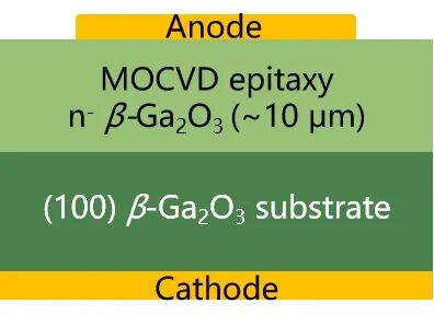
Figure 1 Schematic diagram of the terminal-free SBD device structure
Breakdown Performance: Stable and High Voltage Withstanding Capability
Breakdown voltage is a key parameter for evaluating the voltage endurance of power devices and directly determines their maximum operating voltage. Validation results show that the terminal-less SBD devices fabricated on Garen Semi’s thick-film homoepitaxial wafers achieved breakdown voltages ranging from 1090 to 1490 V, significantly outperforming comparable products from leading Japanese companies.
The results demonstrate the low defect density and high material reliability of Garen Semi’s epitaxial wafers, confirming their suitability for ultra-high-voltage and high-power semiconductor device applications.
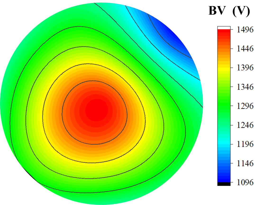
Figure 2 In-plane distribution of breakdown voltage across the SBD device
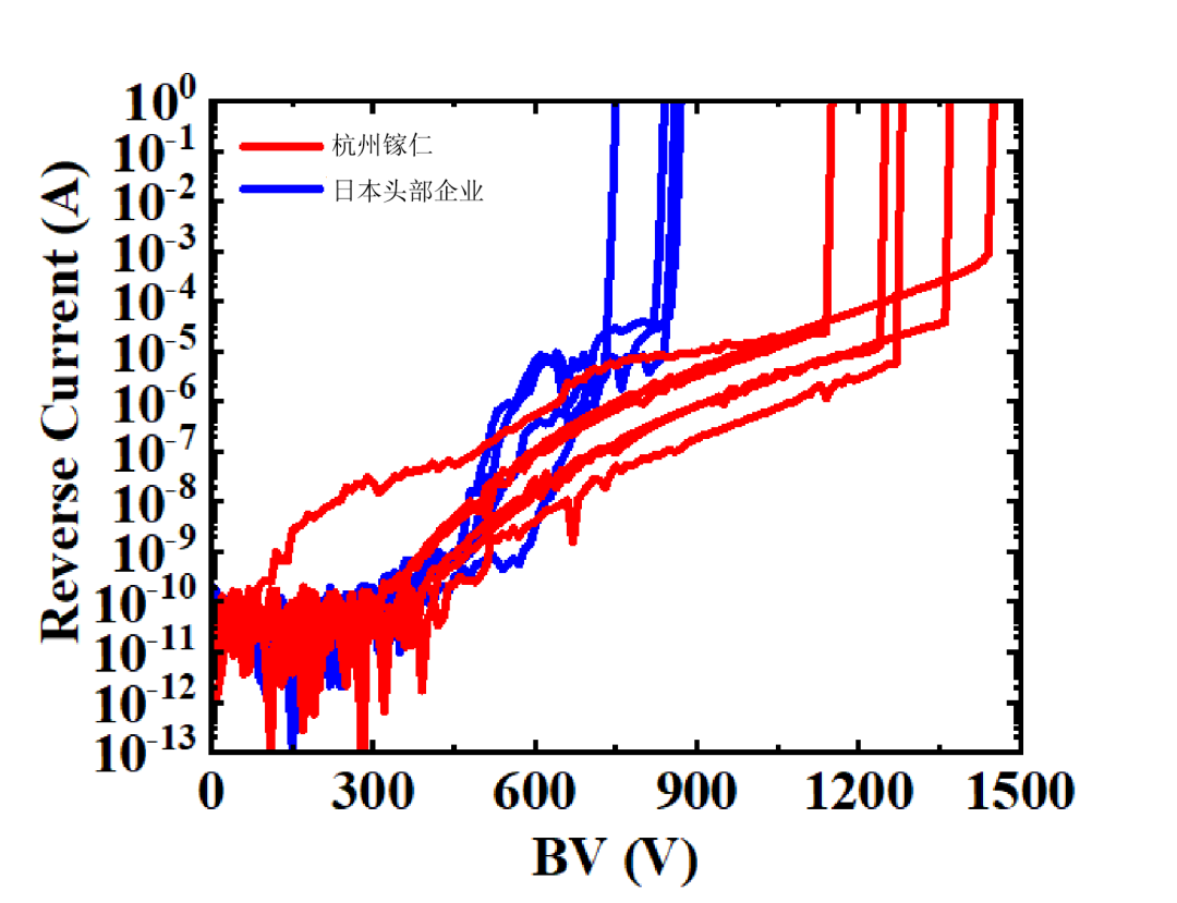
Figure 3 Comparison of SBD breakdown characteristics between Garen Semi and leading Japanese companies
Excellent On-State Performance: Superior Control of Specific On-Resistance
Specific on-resistance is a critical parameter that determines conduction losses in power devices. A lower value indicates reduced energy loss during operation and higher conversion efficiency. The SBD devices fabricated from Garen Semi’s homoepitaxial wafers achieved a specific on-resistance of 2.6–4.5 mΩ·cm², significantly lower than comparable products from leading Japanese companies. These devices simultaneously demonstrate excellent conduction performance and voltage-blocking capability, achieving an optimized balance between low conduction loss and high breakdown voltage.
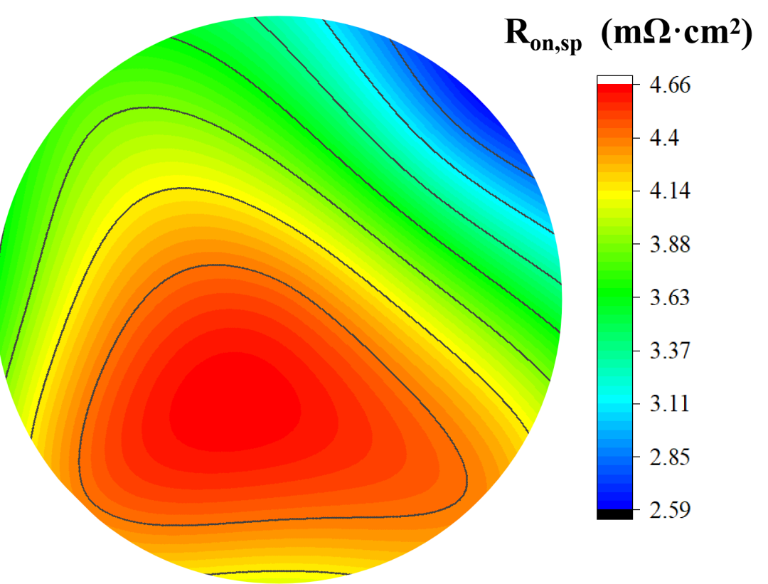
Figure 4 In-plane distribution of SBD device-specific on-resistance
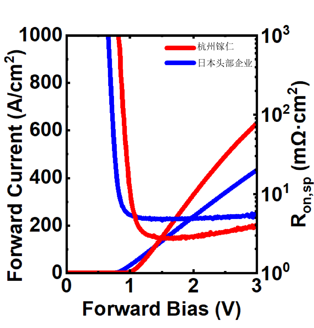
Figure 5 Comparison of Forward Conduction Characteristics of SBD Devices from Garen Semi and Leading Japanese Companies
China’s Independent Path: Advancing Breakthroughs Through Self-Reliant Technology
The foundation of device performance lies in a fully self-controlled technological pathway. Rather than simply following mainstream international approaches, Garen Semi adheres to an independent innovation strategy tailored to China’s semiconductor industry needs. Compared with the internationally prevalent edge-defined film-fed growth (EFG) method, the company’s self-developed casting growth method eliminates reliance on expensive iridium crucibles, significantly reducing material costs. Meanwhile, the technology enables independent control over the thermal field during crystal growth, providing greater flexibility in optimizing defect density and doping uniformity. Supported by its proprietary epitaxial growth processes, the company has achieved low defect densities and precise control of carrier concentration.
The latest validation results demonstrate that SBD devices fabricated on Garen Semi’s epitaxial wafers deliver outstanding comprehensive performance, with key device metrics surpassing imported products. These results fully verify the reliability of the epitaxial wafers, highlighting the company’s precise process control capabilities in large-size thick-film epitaxial growth and breaking the long-standing dependence on imported high-end gallium oxide epitaxial materials. Currently, Garen Semi has established a comprehensive portfolio of thick-film epitaxial wafers, with customizable parameters including epitaxial layer thickness, carrier concentration, and doping type to flexibly meet the development and mass-production requirements of different devices.
Looking ahead, Garen Semi will continue to align with the strategic objectives of China’s 15th Five-Year Plan for accelerating the industrialization of gallium oxide technologies. The company will further optimize growth processes, improve wafer-level uniformity, and accelerate device validation and mass-production introduction of 6-/8-inch epitaxial wafers. By providing high-performance domestic epitaxial materials, Garen Semi aims to lower the barriers to gallium oxide device development and deliver reliable material solutions to support the large-scale commercialization of gallium oxide power devices.
About Garen Semiconductor
Hangzhou Garen Semiconductor Co., Ltd. is a global provider of gallium oxide materials and equipment solutions, specializing in the R&D and commercialization of ultra-wide-bandgap semiconductor technologies. The company’s core products include 2–8 inch gallium oxide single crystals and substrates (including the world’s first 8-inch products), vertical Bridgman (VB) gallium oxide crystal growth equipment, and 2–8 inch gallium oxide homoepitaxial wafers (including the world’s first 8-inch products). Garen Semiconductor is dedicated to building a fully integrated “equipment–crystal growth–substrate–epitaxy” industrial ecosystem and providing comprehensive solutions for global customers. The company’s achievements in gallium oxide have been widely recognized and featured by leading media outlets, including People’s Daily, Xinhua News Agency, Science and Technology Daily, Sina Finance, China Blue News, and The Paper.
For more information, please visit the official website: http://garen.cc/
Or contact us:
Mr. Jiang
Phone: +86 159 1871 9807
Email: jiangjiwei@garen.cc
Mr. Xia
Phone: +86 190 1127 8792
Email: xianing@garen.cc
Instruction
Official Account

Cooperation
Top
