


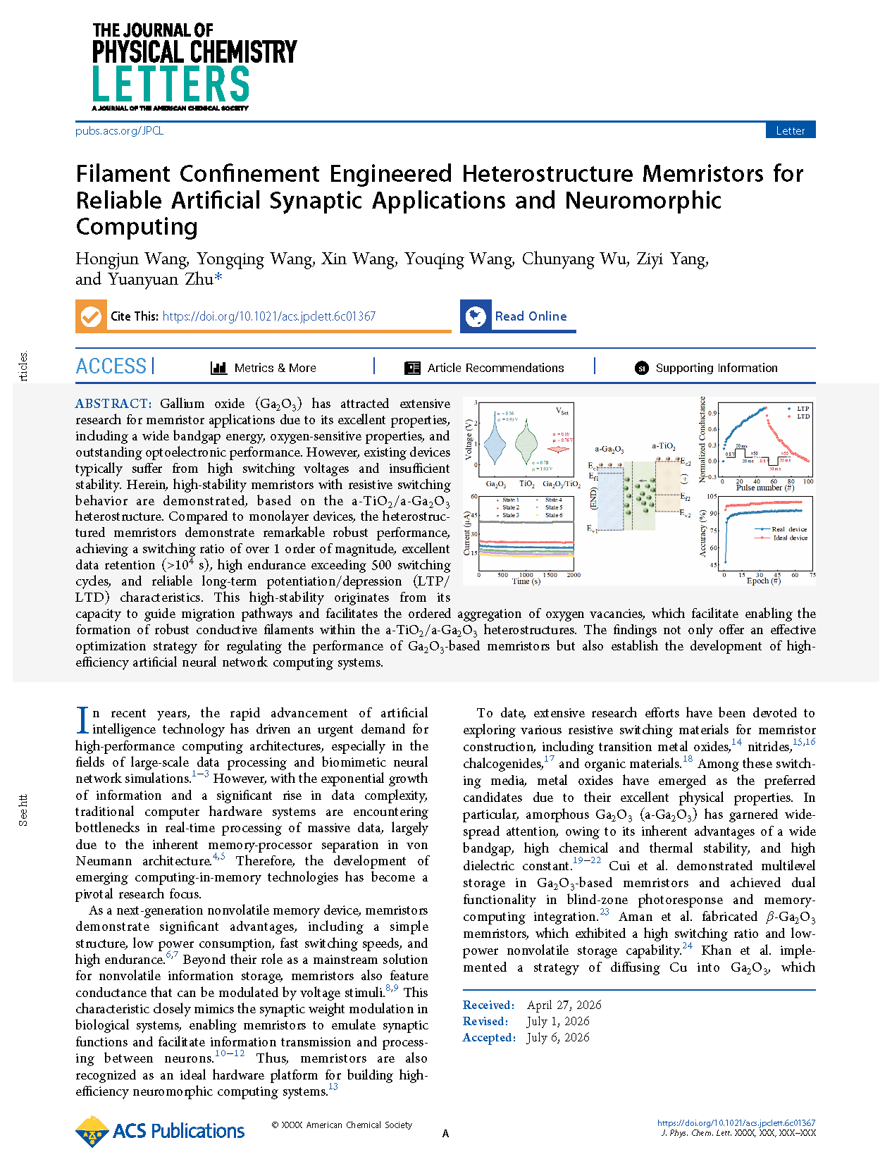
Researchers from Shaanxi University of Science and Technology have published a paper titled "Filament Confinement Engineered Heterostructure Memristors for Reliable Artificial Synaptic Applications and Neuromorphic Computing" in The Journal of Physical Chemistry Letters.
Background
The rapid advancement of artificial intelligence creates urgent demand for in-memory computing hardware. Traditional von Neumann architecture suffers from the separation of memory and processor, leading to low efficiency in massive data real-time processing. Memristors feature simple structure, low power consumption, fast switching speed and voltage-tunable conductance, which can mimic biological synaptic weight modulation and serve as core hardware for neuromorphic computing. Amorphous Ga₂O₃ possesses a wide bandgap and outstanding chemical & thermal stability, making it a promising resistive switching medium. However, monolayer Ga₂O₃ memristors suffer from severe switching voltage fluctuation, poor cycle stability and limited continuous conductance modulation, which restrict the construction of high-precision artificial neural networks. Most existing optimization strategies only modify single-layer films, while the confinement mechanism of conductive filaments in heterostructures lacks systematic investigation. In this work, an a-TiO₂/a-Ga₂O₃ bilayer heterostructure resistive switching layer is designed. The built-in electric field at the interface regulates oxygen vacancy migration pathways and realizes ordered nucleation of conductive filaments. Electrical and synaptic performances of monolayer and heterostructure devices are systematically compared, and the stability improvement mechanism originating from interfacial band alignment is clarified. This work provides an interface engineering strategy for high-reliability wide-bandgap oxide memristors and brain-inspired computing devices.
Abstract
Gallium oxide (Ga₂O₃) has attracted extensive research for memristor applications due to its excellent properties, including a wide bandgap energy, oxygen-sensitive properties, and outstanding optoelectronic performance. However, existing devices typically suffer from high switching voltages and insufficient stability. Herein, high-stability memristors with resistive switching behavior are demonstrated, based on the a-TiO₂ / a-Ga₂O₃ heterostructure. Compared to monolayer devices, the heterostructured memristors demonstrate remarkable robust performance, achieving a switching ratio of over 1 order of magnitude, excellent data retention (>10⁴ s), high endurance exceeding 500 switching cycles, and reliable long-term potentiation/depression (LTP/LTD) characteristics. This high-stability originates from its capacity to guide migration pathways and facilitates the ordered aggregation of oxygen vacancies, which facilitate enabling the formation of robust conductive filaments within the a-TiO₂ / a-Ga₂O₃ heterostructures. The findings not only offer an effective optimization strategy for regulating the performance of Ga₂O₃-based memristors but also establish the development of high-efficiency artificial neural network computing systems.
Highlights
A bilayer a-TiO₂/ a-Ga₂O₃ heterostructure memristor is constructed. The interfacial built-in electric field confines oxygen vacancies to form ordered conductive filaments, solving poor stability and voltage fluctuation of monolayer Ga₂O₃ devices;
The heterostructure achieves over one order of magnitude higher switching ratio, retention time >10⁴s and endurance over 500 cycles. The standard deviation of Set / Reset voltage is greatly reduced for better device uniformity;
Complete biological synaptic behaviors including paired-pulse facilitation (PPF), long-term potentiation / depression (LTP/LTD) are fully emulated, with continuously linear conductance modulation under pulse stimulation;
Band alignment and charge transport fitting verify that the interfacial potential barrier regulates carrier transport, clarifying the physical mechanism of conductive filament confinement and stability improvement;
A three-layer perceptron neural network built on this device reaches 92.65% recognition accuracy on MNIST handwritten digits, showing practical potential for neuromorphic computing.
Conclusion
In summary, we have developed high-stability resistive switching memristors by designing an a-TiO₂ / a-Ga₂O₃ heterostructure. The results demonstrate that heterostructured memristors exhibit remarkable robust performance, including a switching ratio of over 1 order of magnitude, excellent data retention (>10⁴ s), high endurance exceeding 500 switching cycles, multilevel conductance modulation capability, and reliable LTP/LTD characteristics. We propose that the RS mechanism underlying the enhanced switching performance stems from the unique space charge region induced by the TiO₂ interlayer, in which the local electronic states are modulated, and robust CFs are tailed within the engineered a-TiO₂ / a-Ga₂O₃ heterostructures. Finally, a biosynapse-inspired artificial neural network based on a-Ga₂O₃ / a-TiO₂ memristors was demonstrated, achieving a high recognition accuracy of up to 92.65% in the classifying handwritten digit images task. This work demonstrates a heterostructure strategy that enhances the switching performance of a-Ga₂O₃ memristors, advancing their potential for storage and neuromorphic computing applications.
Project Support
This work was supported by the Key Scientific Research Program of Shaanxi Provincial Department of Education (No. 25JR033), Natural Science Foundation of Shaanxi Province (No. 2025JC-YBMS-001), National Natural Science Foundation of China (No. 11905119), Innovation Capability Support Program of Shaanxi (No. 2024CX-GXPT-21), and the Youth Innovation Team of Shaanxi Universities.
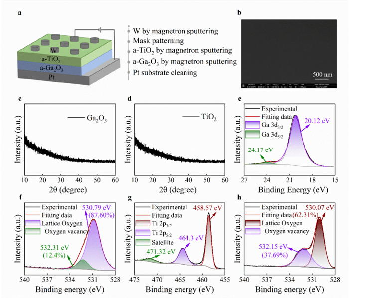
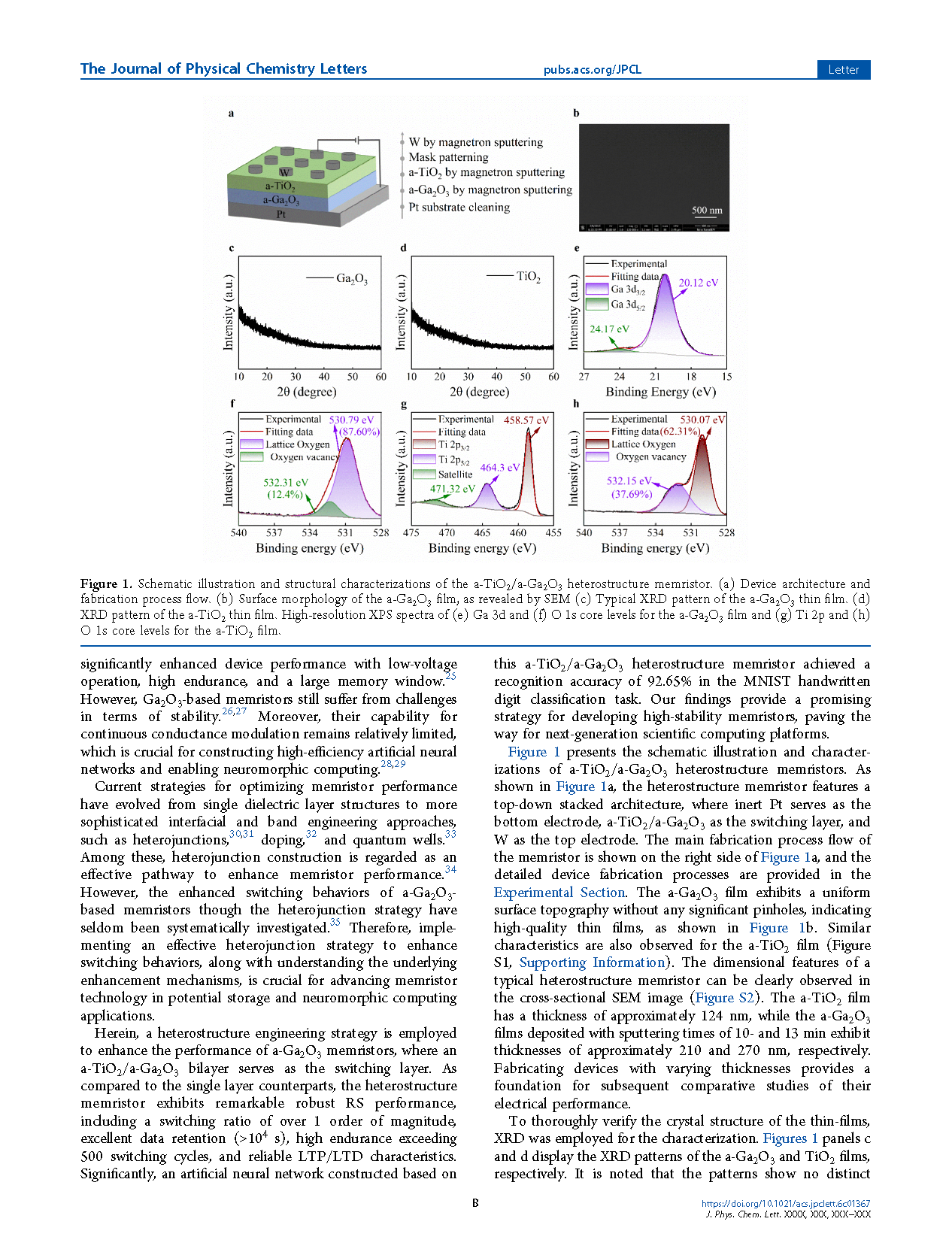
Figure 1 (a) Schematic diagram of W / a-TiO₂ / a-Ga₂O₃ / Pt heterostructure device and fabrication process; (b) SEM surface morphology of a-Ga₂O₃ thin film; (c) XRD pattern of a-Ga₂O₃; (d) XRD pattern of a-TiO₂; (e) High-resolution Ga 3d XPS spectrum of a-Ga₂O₃; (f) High-resolution O 1s XPS spectrum of a-Ga₂O₃; (g) High-resolution Ti 2p XPS spectrum of a-TiO₂; (h) High-resolution O 1s XPS spectrum of a-TiO₂
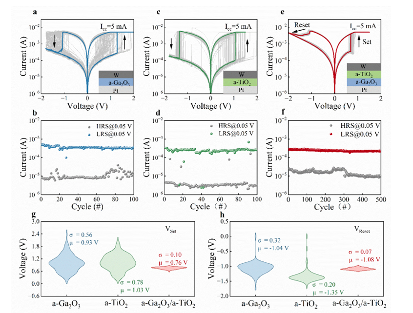
Figure 2 (a) Cyclic I-V curves of monolayer a-Ga₂O₃ device; (b) Endurance property of monolayer a-Ga₂O₃; (c) Cyclic I-V curves of monolayer a-TiO₂ device; (d) Endurance property of monolayer a-TiO₂; (e) Cyclic I-V curves of a-TiO₂ / a-Ga₂O₃ heterostructure; (f) Endurance property of heterostructure device; (g) Statistical distribution of V_Set for three types of devices; (h) Statistical distribution of V_Reset for three types of devices
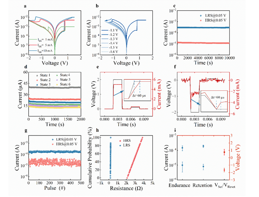
Figure 3 (a) I-V characteristics of heterostructure under different compliance currents; (b) I-V curves under successive negative sweeps; (c) Retention curves of HRS and LRS for 10⁴ s; (d) Retention performance under various reset voltages; (e) Switching response time of Set process; (f) Switching response time of Reset process; (g) 500-cycle pulse endurance; (h) Cumulative probability distribution of resistance states; (i) Statistical switching parameters of 30 random devices
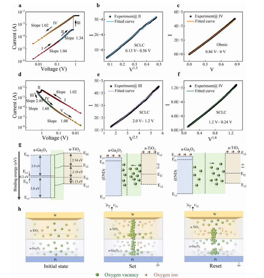
Figure 4 (a) Logarithmic I-V fitting under positive bias; (b) I versus V¹·³ relation in high-resistance state; (c) Ohmic conduction fitting of low-resistance state; (d) Logarithmic I-V curves under negative bias; (e) I-V²·⁵ fitting of HRS under negative voltage; (f) I-V¹·⁶ fitting for medium-high resistance region; (g) Schematic band alignment of the heterojunction; (h) Evolution model of oxygen vacancy conductive filaments at initial, Set and Reset states
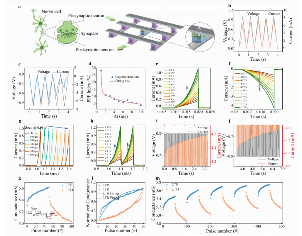
Figure 5 (a) Schematic of memristor-based artificial synapse; (b) Synaptic potentiation triggered by continuous triangular pulses; (c) Synaptic depression triggered by continuous triangular pulses; (d) Paired-pulse facilitation (PPF) characteristic; (e) EPSC induced by positive pulses with different amplitudes; (f) IPSC induced by negative pulses with different amplitudes; (g) Pulse width-dependent EPSC; (h) Amplitude-dependent EPSC under paired pulses; (i) Conductance increase under successive positive pulses; (j) Conductance decrease under successive negative pulses; (k) Long-term potentiation and depression (LTP/LTD); (l) Nonlinear fitting of synaptic weight; (m) Conductance modulation under alternating pulse cycles
DOI:
doi.org/10.1021/acs.jpclett.6c01367
Instruction
Official Account

Cooperation
Top
