


The 19th National Conference on MOCVD will be held from July 27 to 29, 2026, in Hohhot, Inner Mongolia, China. The conference will focus on five major topics: “Material Growth, Characterization and Equipment,” “Power Electronics and RF Devices,” “Optoelectronic Devices and Applications,” “Ultra-Wide-Bandgap Semiconductors and Frontier Interdisciplinary Research,” and “Emerging Devices and New Applications for AI and Beyond.” The event aims to provide a high-level platform for MOCVD technology exchange, industrial synergy, and the commercialization of achievements.
Hangzhou Garen Semiconductor Co., Ltd. (hereinafter “Garen Semi”) has been invited to participate in this conference, where it will engage in in‑depth exchanges with experts and colleagues from universities, research institutes, and the industrial chain upstream and downstream, jointly discussing key issues in gallium oxide material growth, epitaxial tuning, and industrial applications.
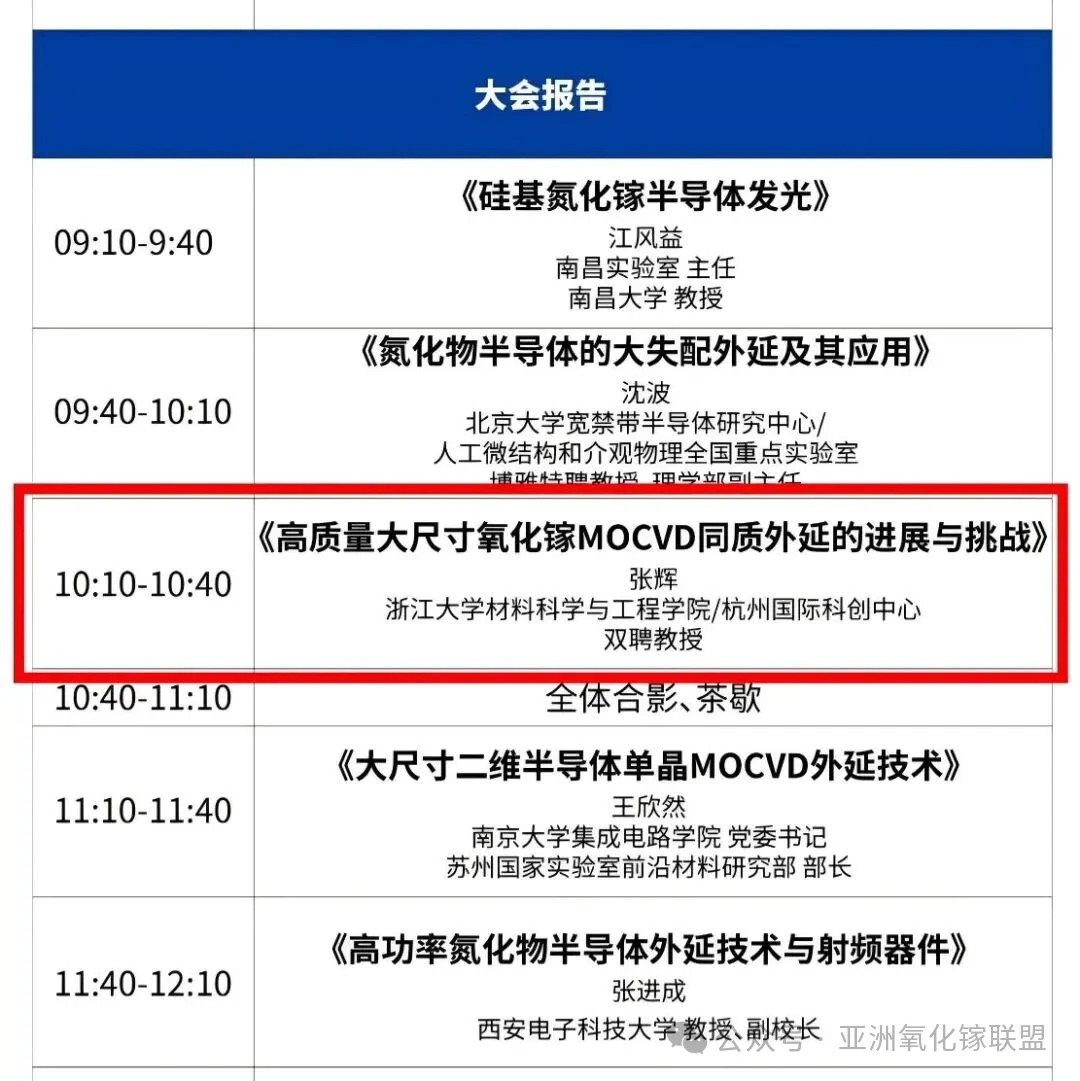
During the conference, Professor Zhang Hui — who holds a joint appointment at the School of Materials Science and Engineering of Zhejiang University and the Hangzhou International Science and Technology Innovation Center, and serves as Chairman of Garen Semi — will deliver a plenary presentation on the morning of July 28. His talk, focusing on the theme of “Progress and Challenges in High‑Quality Large‑Size Gallium Oxide MOCVD Homoepitaxy”, will share cutting‑edge advances and industrialization perspectives in the field of large‑size gallium oxide homoepitaxy.
On the occasion of this industry gathering, Garen Semi will simultaneously launch a limited‑time promotional offer on gallium oxide epitaxial wafers, providing research institutes, universities, and device manufacturers with high‑quality material support through an expanded product portfolio and more competitive pricing. For detailed product information and discount terms, you are welcome to contact us and discuss during the conference.
From single‑crystal growth and substrate preparation to epitaxial processing, Garen Semi consistently adheres to an independent technological roadmap and continuously advances the engineering and large‑scale application of gallium oxide materials. We look forward to meeting colleagues from all sectors in Hohhot to explore the technological frontier and the future of the industry together. July 27–29 – Garen Semi awaits you at the 19th National MOCVD Academic Conference!
About Garen Semiconductor
Hangzhou Garen Semiconductor Co., Ltd. is a global provider of gallium oxide materials and equipment solutions, specializing in the R&D and commercialization of ultra-wide-bandgap semiconductor technologies. The company’s core products include 2–8 inch gallium oxide single crystals and substrates (including the world’s first 8-inch products), vertical Bridgman (VB) gallium oxide crystal growth equipment, and 2–8 inch gallium oxide homoepitaxial wafers (including the world’s first 8-inch products). Garen Semiconductor is dedicated to building a fully integrated “equipment–crystal growth–substrate–epitaxy” industrial ecosystem and providing comprehensive solutions for global customers. The company’s achievements in gallium oxide have been widely recognized and featured by leading media outlets, including People’s Daily, Xinhua News Agency, Science and Technology Daily, Sina Finance, China Blue News, and The Paper.
For more information, please visit the official website: http://garen.cc/
Or contact us:
Mr. Jiang
Phone: +86 159 1871 9807
Email: jiangjiwei@garen.cc
Mr. Xia
Phone: +86 190 1127 8792
Email: xianing@garen.cc
Instruction
Official Account

Cooperation
Top
