


On July 24, 2026, the 7th Council Meeting of the 4th Session and the 5th General Membership Meeting of the 4th Session of the Zhejiang Provincial Semiconductor Industry Association were grandly held at the Hangzhou Binjiang Kaiyuan Mingdu Grand Hotel. During the meeting, Hangzhou Fujia Gallium Industry Technology Co., Ltd. was honored with the 2025 Zhejiang Provincial Semiconductor Industry "Zhejiang Core · Qixing Award", and was officially added as a new Governing Board Member Unit of the 4th Zhejiang Provincial Semiconductor Industry Association, with the awarding ceremony completed on site. This recognition fully affirms Fujia Gallium Industry's technological strength, industrial contributions, and industry influence in the eyes of the provincial industry association.
In the past development cycle, Fujia Gallium has not only successfully achieved stable mass production of large-size gallium oxide single-crystal substrates, but also made the world’s first release of a 12-inch gallium oxide single crystal in March of this year, continuously setting new industry size records. At the same time, in the field of MOCVD homoepitaxy, product performance has been steadily iterated. The latest batch of epitaxial wafers shows an average mobility of 209.9 cm²/(V·s) and an average carrier concentration of 3.2×10¹⁶ cm⁻³, with all key indicators ranking at the domestic leading level. These solid data and mass-production achievements have built the core foundation for Fujia Gallium to win the “Qixing Award.”
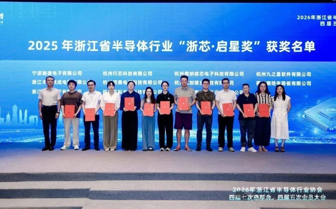
2025 Zhejiang Semiconductor Industry “Zhejiang Core · Qixing Award” Ceremony
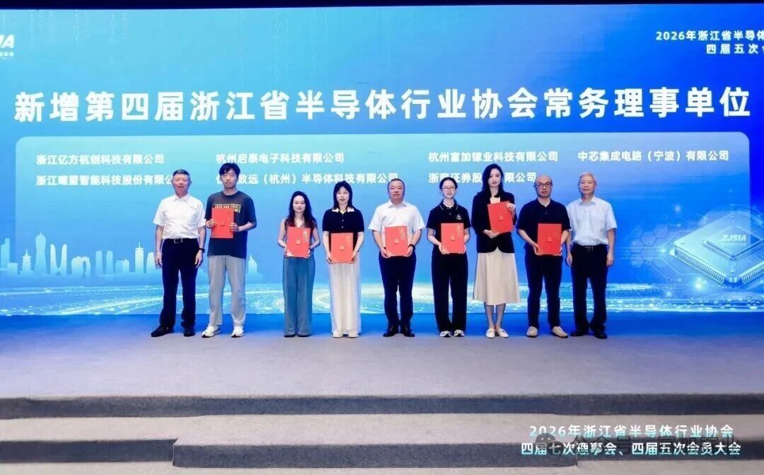
The 4th Zhejiang Provincial Semiconductor Industry Association Governing Board Member Unit Awarding Ceremony
In the future, Fujia Gallium will continue to uphold its mission of “Bringing Better Materials to the World,” deeply cultivate the fourth-generation semiconductor field, and contribute “Fujia power” to the prosperity and development of the global semiconductor industry with even better products and technologies.
Extended Reading—Fujia Gallium Product Milestones
2024.02—Developed China’s first 6-inch conductive gallium oxide single crystal by the Edge‑defined Film‑fed Growth (EFG) method.
2024.05—Gallium oxide “one‑click crystal growth” technology was first featured on CCTV’s Morning News program.
2024.07—Realized China’s first 3-inch VB‑method gallium oxide single‑crystal growth.
2024.12—Realized China’s first 4-inch VB‑method gallium oxide single‑crystal growth.
2025.09—Achieved China’s first breakthrough in 6-inch VB‑method gallium oxide single‑crystal preparation, obtaining the world’s largest gallium oxide single crystal to date.
2025.09—Took the lead in drafting the first national standard in the gallium oxide field, Gallium Oxide Single‑Crystal Polished Wafers.
2025.10—Made another breakthrough in gallium oxide MOCVD homoepitaxy technology; the mobility of a gallium oxide homoepitaxial wafer with thickness exceeding 10 μm reached 181.6 cm²/(V·s), achieving world‑leading performance.
2025.10—Based on the high‑performance MOCVD epitaxial wafers developed, Fuzhou University’s team successfully fabricated a gallium oxide vertical power Schottky barrier diode with the world’s best PFOM (3.07 GW/cm²).
2025.10—Took the lead in China to release a new (011)‑oriented gallium oxide substrate.
2025.12—Developed the world’s first 8‑inch VB‑method gallium oxide single crystal.
2026.01—Co‑founded Shanghai Jiachi Power Technology Co., Ltd., a domestic enterprise focused on gallium oxide devices and modules for end customers.
2026.02—China’s first production line with an annual capacity of 10,000 6/8‑inch gallium oxide single‑crystal epitaxial wafers successfully passed environmental impact assessment acceptance.
2026.03—Became the only Chinese company among the top 15 applicants in global gallium oxide patent counts.
2026.03—Jointly launched, with downstream user Shanghai Gongcheng Semiconductor, a chip‑level packaged and tested gallium oxide diode device for the first time in China.
2026.03—Developed the world’s first 12‑inch gallium oxide single crystal.
2026.06—Launched the world’s first (011)‑oriented 2‑inch gallium oxide substrate.
2026.06—Pioneered the launch of large‑size (011) single‑crystal substrates both in China and globally; substrate quality was jointly verified by the National Institute of Metrology, China, and Shenzhen Pinghu Laboratory, with XRD 5‑point full width at half maximum (FWHM) better than 40 arcsec and optimal values as low as 10 arcsec.
About Hangzhou Fujia Gallium
Hangzhou Fujia Gallium Technology Co., Ltd. was established on December 31, 2019. Guided by the vision of “Bringing Better Materials to the World,” the company is dedicated to the industrialization of ultra-wide-bandgap gallium oxide semiconductor materials. Its core products include gallium oxide single-crystal substrates, MOCVD/MBE epitaxial wafers, and crystal growth equipment based on the Vertical Bridgman (VB) and Edge-Defined Film-Fed Growth (EFG) methods. Recognized as a National High-Tech Enterprise, the company has undertaken multiple national and provincial/ministerial-level projects from the Ministry of Science and Technology, the National Development and Reform Commission, and the Ministry of Industry and Information Technology. It has been authorized nearly 70 international and domestic patents, and serves as the initiator and primary drafter of China's national standards in the field of gallium oxide. The company's series of major achievements in promoting gallium oxide industrialization have been featured in special coverages by prominent media outlets, including CCTV, People’s Daily, Xinhua News Agency, China Securities Journal, and The Paper.
Instruction
Official Account

Cooperation
Top
