


Researchers from the Huazhong University of Science and Technology and Wuhan University and Wuhan University of Technology have published a dissertation titled " Defect distribution in β-Ga₂O₃ single crystal via selective wet etching " in AIP Advances.
Background
Monoclinic Ga₂O₃ is an ultra-wide bandgap semiconductor with a bandgap of approximately 4.8 eV. It possesses ultrahigh breakdown electric field, low on-resistance and the capability of large-size substrate fabrication via melt growth, serving as core material for next-generation high-voltage power devices, ultraviolet photodetectors and neuromorphic devices. Compared with SiC and GaN single crystals, EFG-grown Ga₂O₃ substrates have lower production cost and broad industrialization prospects.
Two kinds of internal crystal defects, dislocations and voids, exert dual effects on Ga₂O₃. From fundamental material perspective, defects induce crystal exfoliation and polymorph transformations. For device application, high-density defects drastically increase leakage current and reduce breakdown voltage, which severely limit the reliability of power devices.
Wet chemical etching is a convenient and reliable characterization method for single crystal quality. Three mainstream etchants H₃PO₄, KOH and molten KOH+NaOH are widely used in industry. Existing researches have many deficiencies: etchant evaporates under high temperature and long etching time, leading to unstable concentration and poor experimental repeatability; etch pits induced by voids and dislocations cannot be clearly distinguished; systematic comparison of defects on four commercial mainstream orientations (100), (010), (001) and (2̅01) is absent; standardized optimal parameters of etchant concentration, temperature and etching time have not been established; etch pits distribute extremely unevenly, and counting based on a small number of local images brings huge statistical error; the intrinsic mechanisms of orientation-dependent dislocation configurations, three-dimensional defect distribution and anisotropic etching remain unclear, without quantitative conclusion of optimal substrate orientation for devices.
In this work, a distillation reflux constant-temperature etching device is constructed to stabilize etchant concentration throughout the experiment. Commercial EFG-polished Ga₂O₃ single crystals with four orientations (100), (010), (001) and (2̅01) are adopted. Combined with OM, SEM, FIB-TEM/STEM characterization, this paper systematically studies the formation mechanism of etch pits, three-dimensional distribution of defects, time-dependent evolution of etching patterns, clarifies the root of anisotropic etching, establishes a standardized measurement scheme for defect density, and identifies the preferential orientation with the minimum dislocation density for device fabrication.
Abstract
Dislocation density in Ga₂O₃ has been determined by chemical etching for four (100), (010), (001), and (2̅01) orientated samples by employing a distillation apparatus to maintain the etch conditions where dislocations and voids can be well identified. Severe non-uniform distribution of etch pits was found where mean and standard deviation of dislocation density from a large amount of measurements are proposed for evaluating the quality of the Ga₂O₃ single crystal. It was found that (001) orientated sample has the minimum mean dislocation density around 10³ cm⁻², one order less than the other orientated samples. Intertwined dislocations for the (010) orientated sample, single dislocation lying on (100) for the (001) orientated sample, and a stack of dislocations lying on the (2̅01) plane for the (100) orientated sample have been observed. The anisotropy growth of dislocations and voids, their migration and interaction, and direction-dependent etch rate are believed to be the root cause for the formation of a variety of etch patterns and orientation-related dislocation densities. With higher etchant concentration, less etch time and lower magnification images are suggested for accurately computing the etch pit density.
Highlights
A self-designed distillation etching equipment with condensation reflux is proposed to eliminate concentration fluctuation of H₃PO₄, KOH and molten KOH+NaOH caused by high-temperature evaporation, maintain stable etching conditions throughout experiments and greatly improve the repeatability of defect measurement.
Systematic comparison of etching behaviors on four commercial EFG-grown Ga₂O₃ orientations (100), (010), (001) and (2̅01) is performed. FIB-TEM directly distinguishes etch pits induced by voids and dislocations, and unique dislocation configurations on each plane are clarified: intertwined dislocations on (010), single dislocations on (100) plane for (001) samples, stacked dislocations on (2̅01) plane for (100) samples.
Dynamic transformation rule of etch pits is uncovered: pits derived from voids and dislocations can mutually convert under prolonged etching, originating from three-dimensional depth distribution difference of bulk defects. The anisotropic etching rate sequence of Ga₂O₃ is quantitatively confirmed: (010) > (001) > (100).
Quantitative measurement verifies that (001)-oriented Ga₂O₃ possesses dislocation density as low as 10³ cm⁻², one order of magnitude lower than other orientations, confirming it as the optimal substrate for power device fabrication.
A standardized crystal quality evaluation system is established: high-concentration etchant with short etching time and low-magnification images for pit counting; mean value plus standard deviation from multiple measurements is adopted to eliminate statistical error caused by uneven local distribution of etch pits.
Conclusion
In this paper, we report that distribution of defects, mainly voids and dislocations, on the four orientated Ga₂O₃ samples can be well identified and determined by high quality images taken by optical microscopy via surface etching. A set of distillation apparatus was implemented for maintaining etchant concentration during high temperature and long time etching. The preferential orientation for fabrication of the Ga₂O₃-based device with the minimum dislocation density was found. The anisotropy growth of dislocations and voids, their migration and interaction, and direction-dependent etch rate are believed to be the root cause for the formation of variety of etch patterns and orientation related dislocation densities. The higher etchant concentration, less etch time, and lower magnification images are suggested for accurately computing the etch pit density.
Project Support
This work was supported by the Major Program (JD) of Hubei Province under Grant No. 2023BAA009.
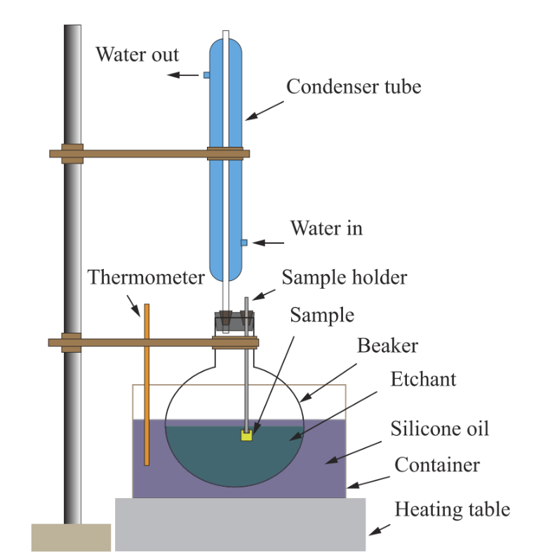
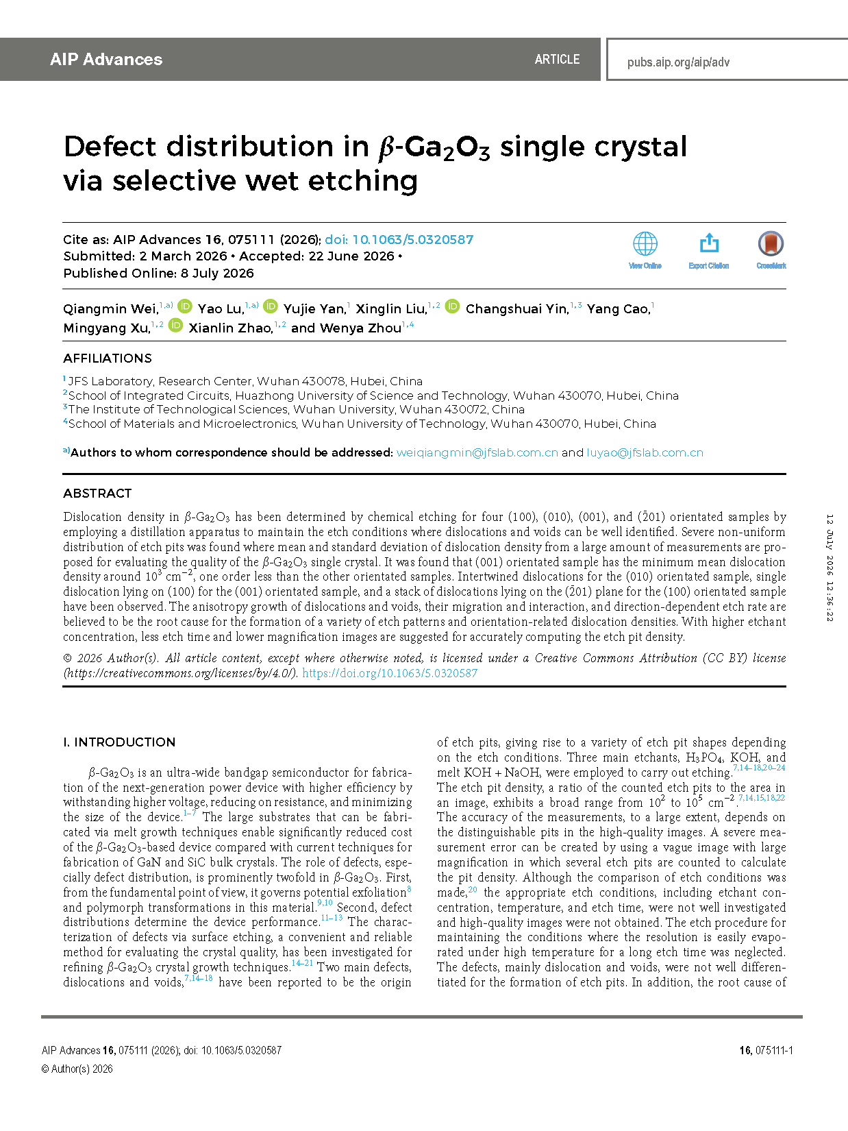
Fig. 1. Schematic illustration of the instrument for Ga₂O₃ etching.
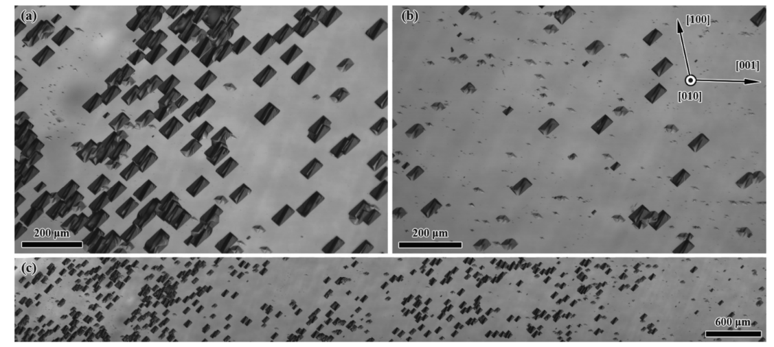
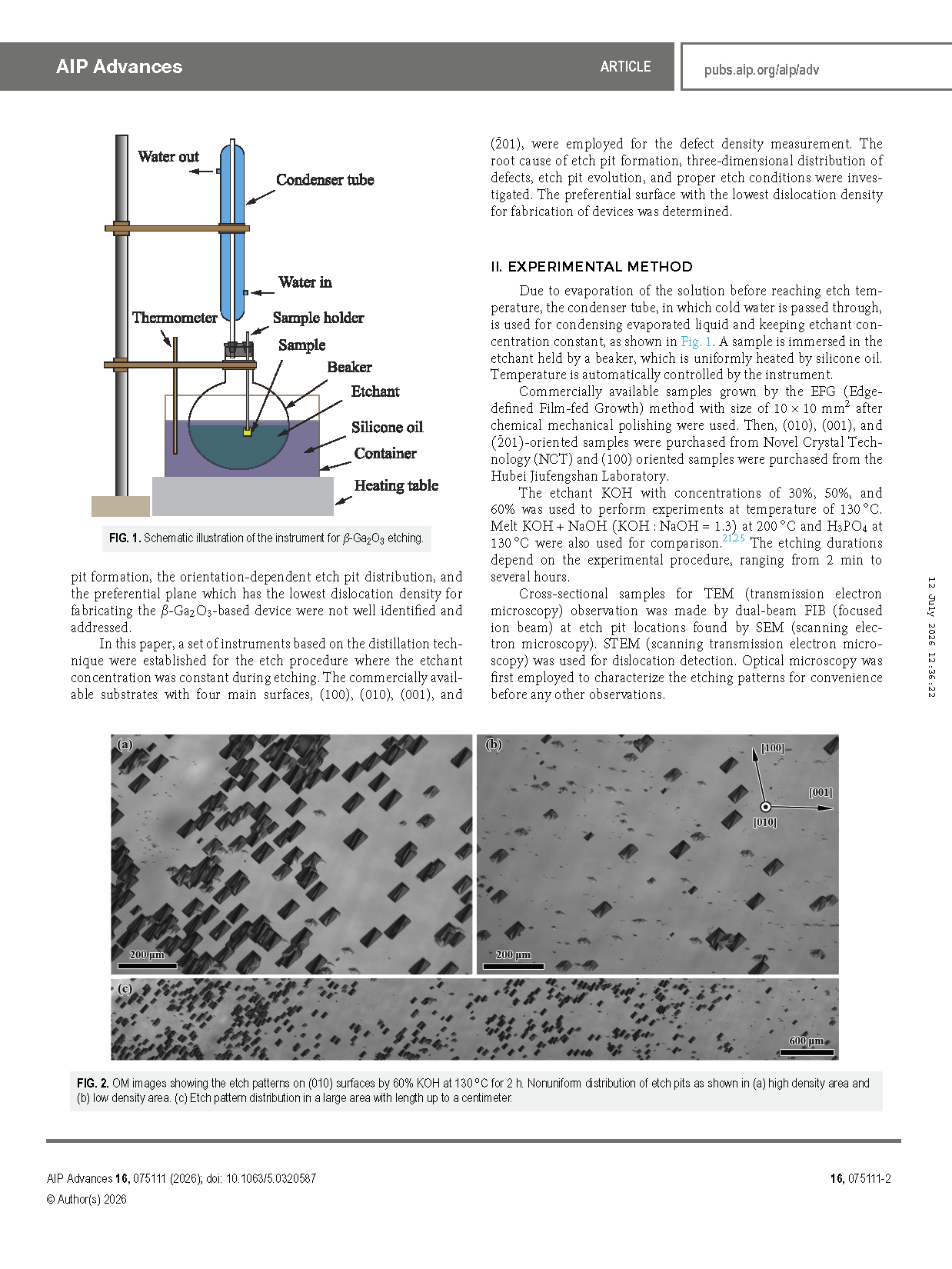
Fig. 2. OM images showing the etch patterns on (010) surfaces by 60% KOH at 130 °C for 2 h. Nonuniform distribution of etch pits as shown in (a) high density area and (b) low density area. (c) Etch pattern distribution in a large area with length up to a centimeter.
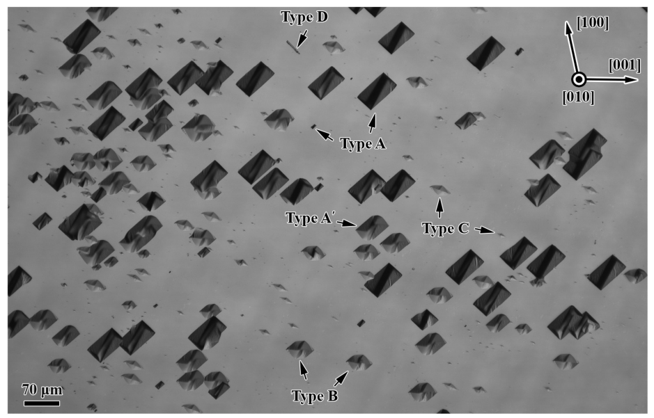
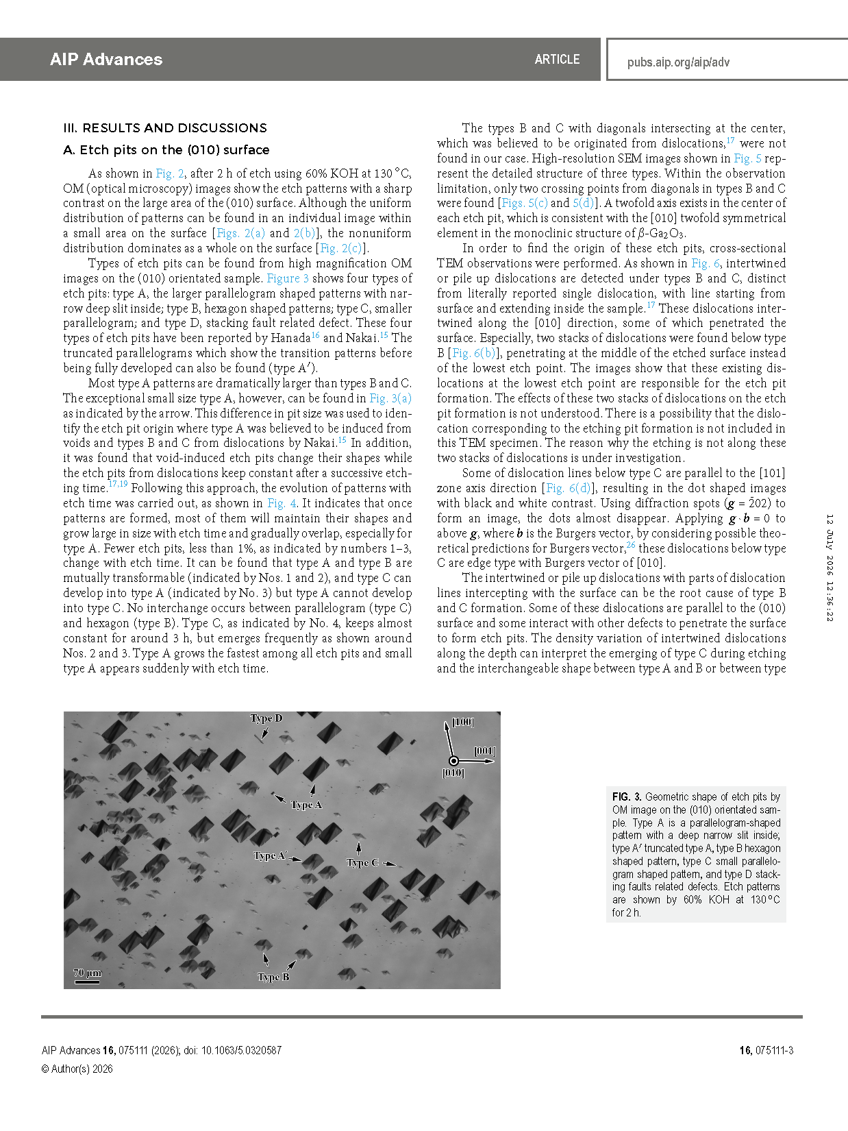
Fig. 3. Geometric shape of etch pits by OM image on the (010) orientated sample. Type A is a parallelogram-shaped pattern with a deep narrow slit inside; type A′ truncated type A, type B hexagon shaped pattern, type C small parallelogram shaped pattern, and type D stacking faults related defects. Etch patterns are shown by 60% KOH at 130 °C for 2 h.
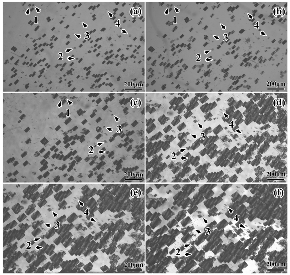
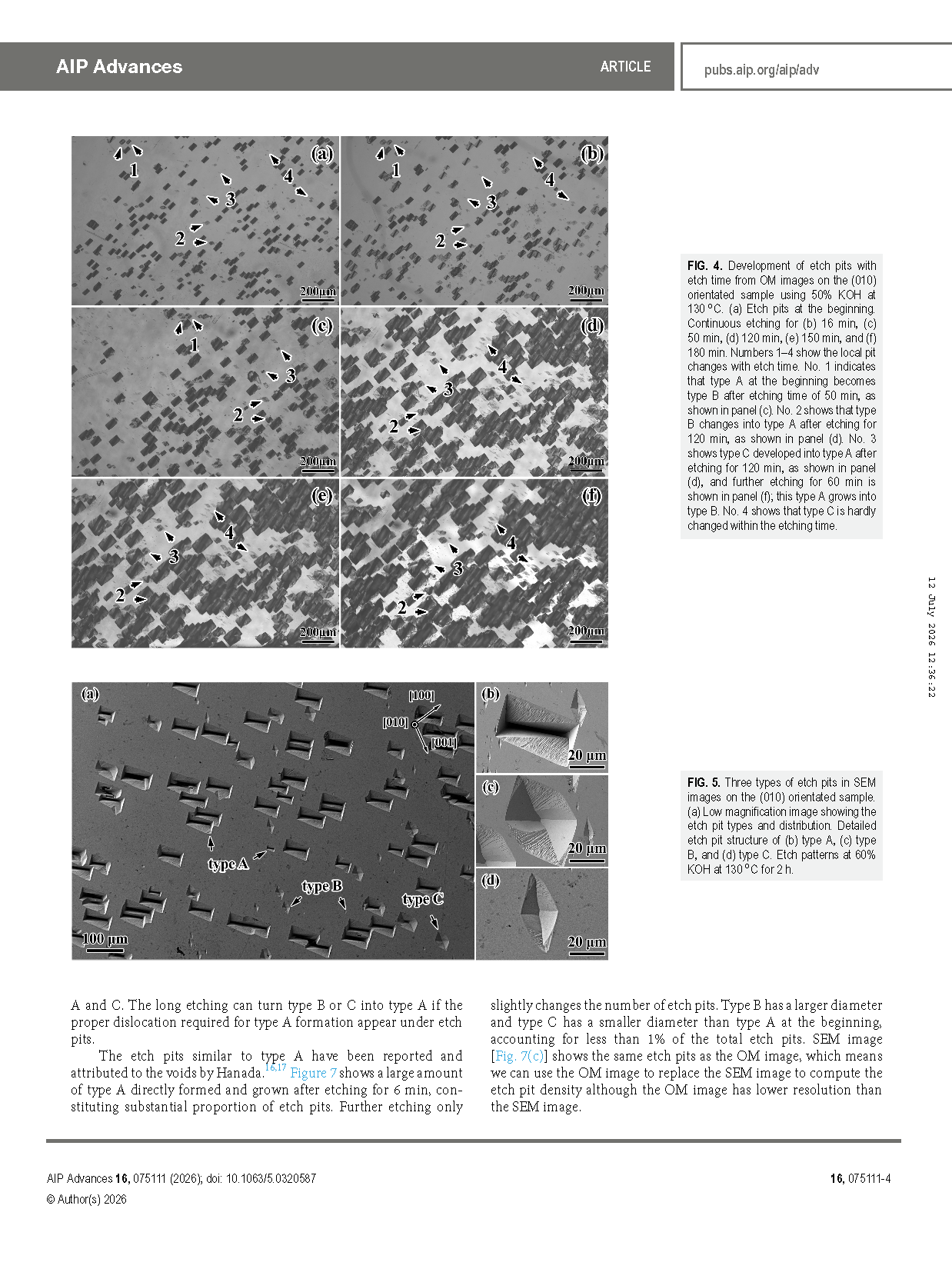
Fig. 4. Development of etch pits with etch time from OM images on the (010) orientated sample using 50% KOH at 130 °C. (a) Etch pits at the beginning. Continuous etching for (b) 16 min, (c) 50 min, (d) 120 min, (e) 150 min, and (f) 180 min. Numbers 1–4 show the local pit changes with etch time. No.1 indicates that type A at the beginning becomes type B after etching time of 50 min, as shown in panel (c). No. 2 shows that type B changes into type A after etching for 120 min, as shown in panel (d). No.3 shows type C developed into type A after etching for 120 min, as shown in panel (d), and further etching for 60 min is shown in panel (f); this type A grows into type B. No.4 shows that type C is hardly changed within the etching time.
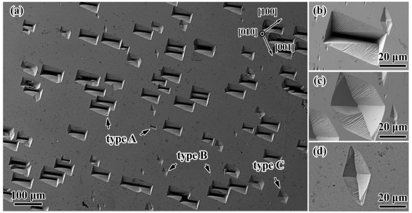
Fig. 5. Three types of etch pits in SEM images on the (010) orientated sample. (a) Low magnification image showing the etch pit types and distribution. Detailed etch pit structure of (b) type A,(c) type B,and (d) type C. Etch patterns at 60% KOH at 130 °C for 2 h.
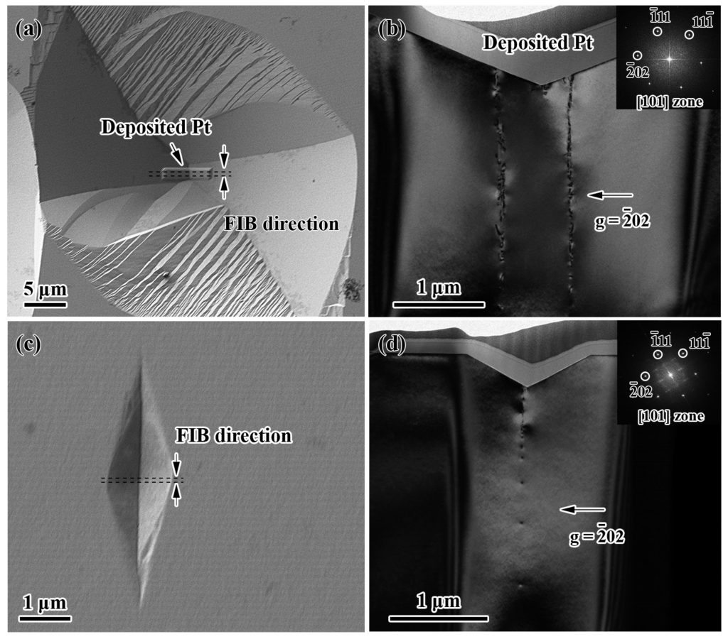
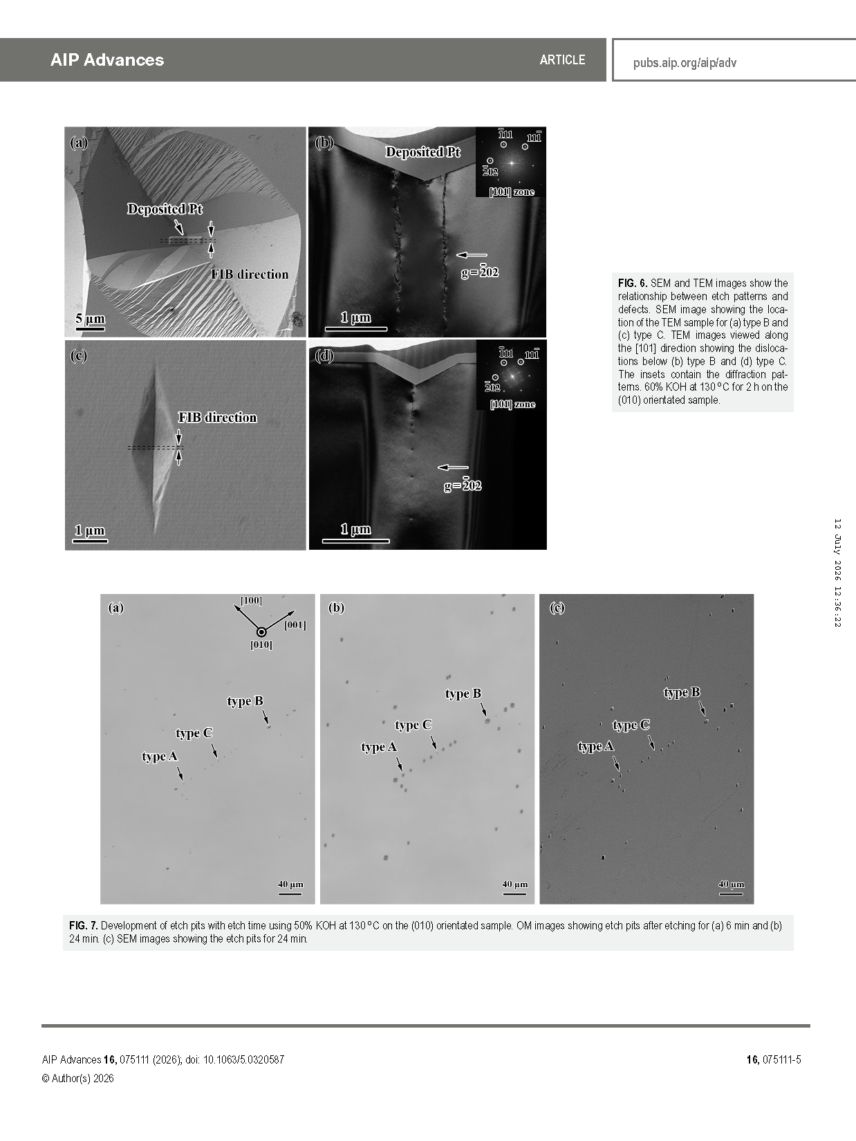
Fig. 6. SEM and TEM images show the relationship between etch patterns and defects. SEM image showing the location of the TEM sample for (a) type B and (c) type C. TEM images viewed along the [101] direction showing the dislocations below (b) type B and (d) type C. The insets contain the diffraction patterns. 60% KOH at 130 °C for 2 h on the (010) orientated sample.
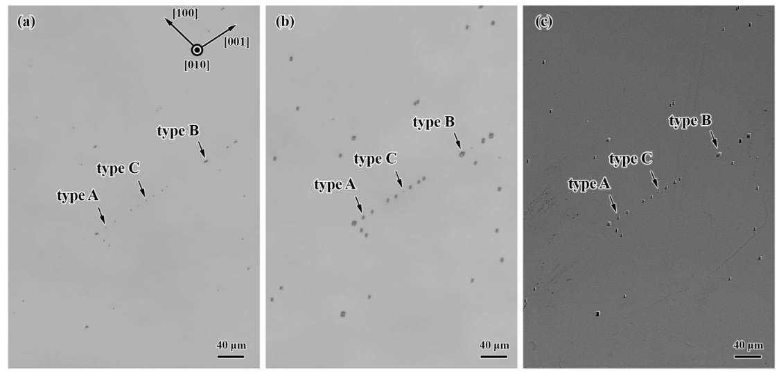
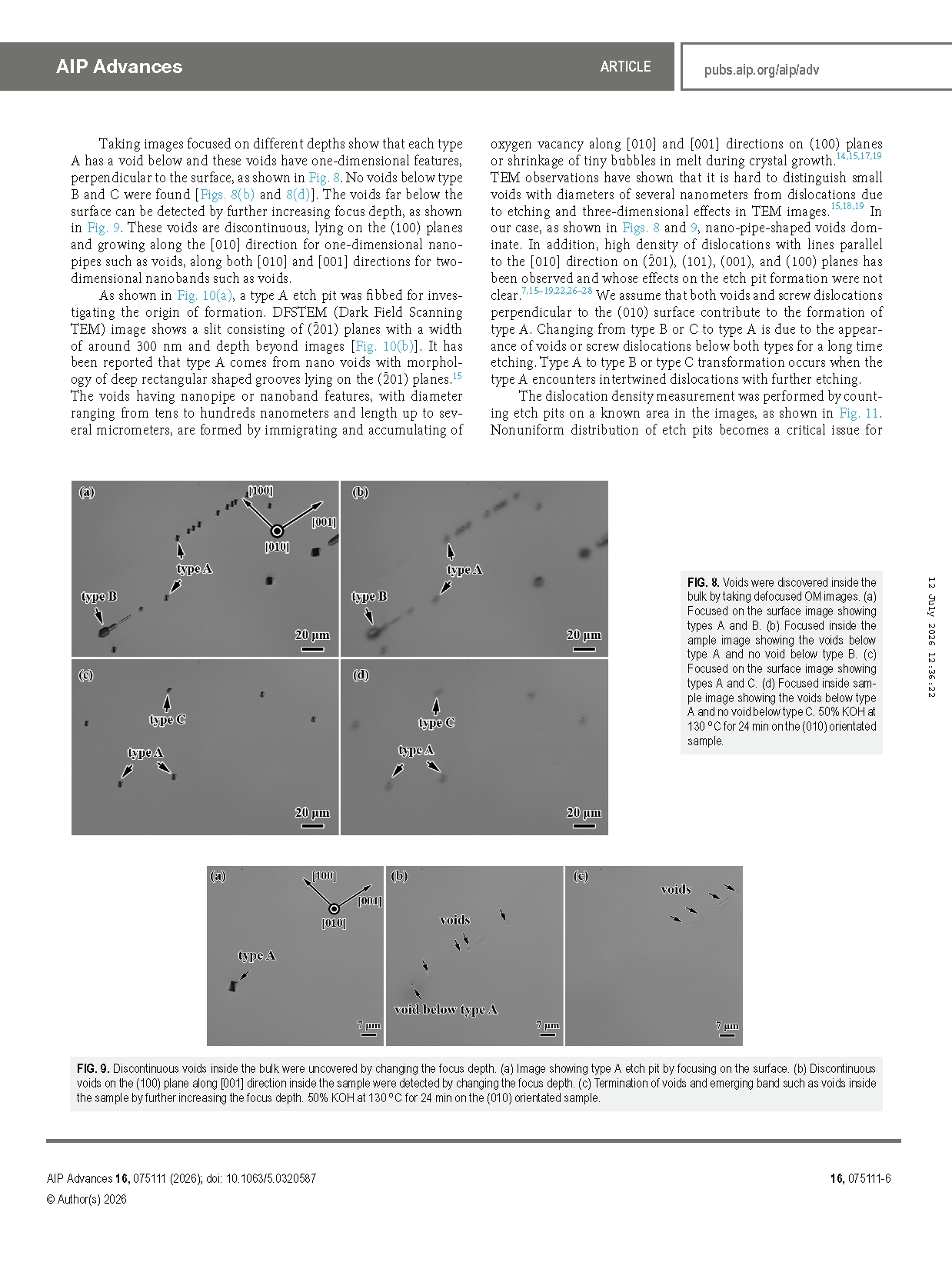
Fig. 7. Development of etch pits with etch time using 50% KOH at 130 °C on the (010) orientated sample. OM images showing etch pits after etching for (a) 6 min and (b) 24 min. (c) SEM images showing the etch pits for 24 min.
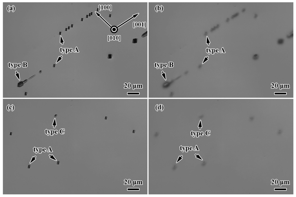
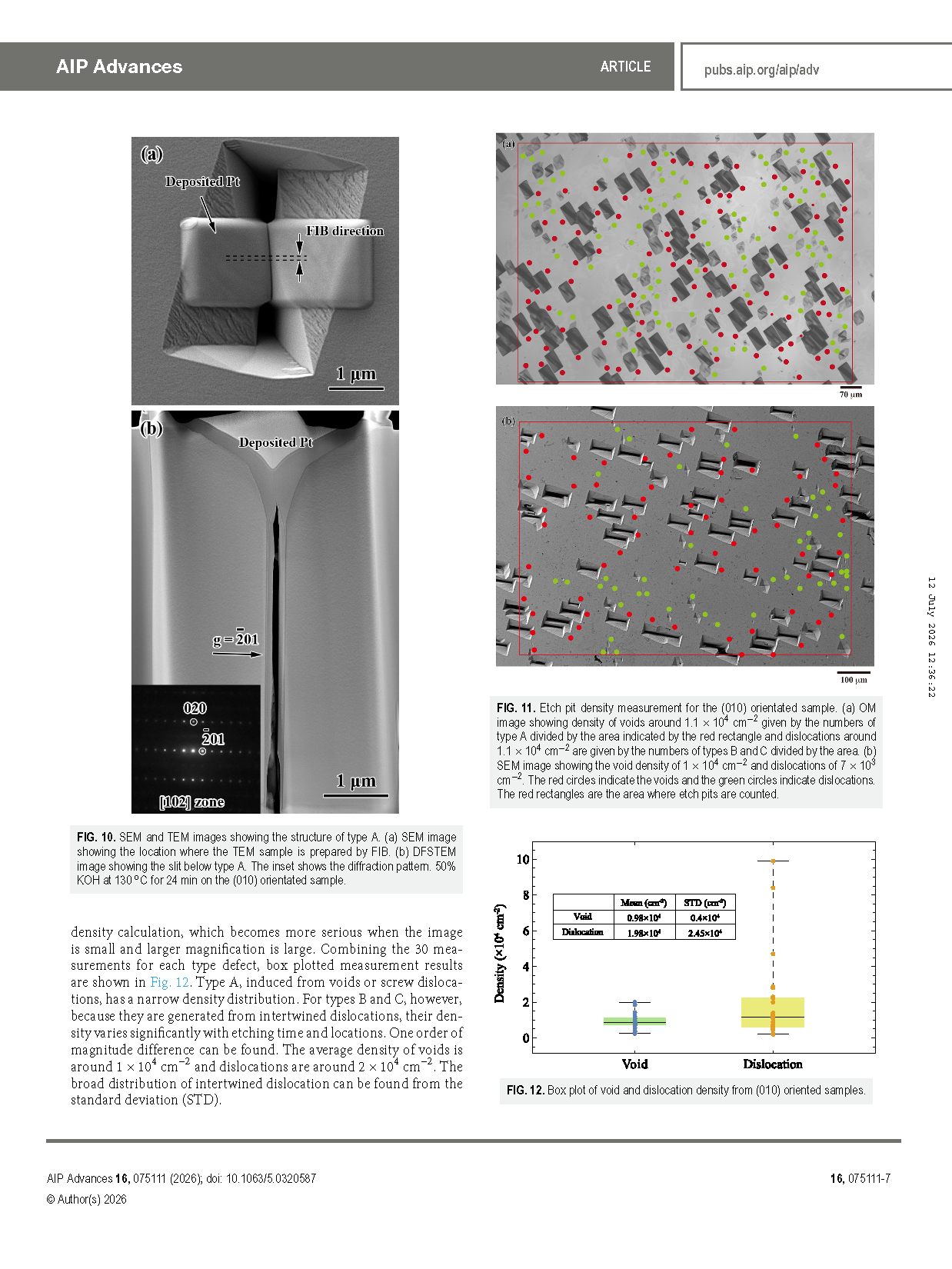
Fig. 8. Voids were discovered inside the bulk by taking defocused OM images.(a) Focused on the surface image showing types A and B.(b) Focused inside the sample image showing the voids below type A and no void below type B. (c) Focused on the surface image showing types A and C.(d) Focused inside sample image showing the voids below type A and no void below type C. 50% KOH at 130 °C for 24 min on the (010) orientated sample.
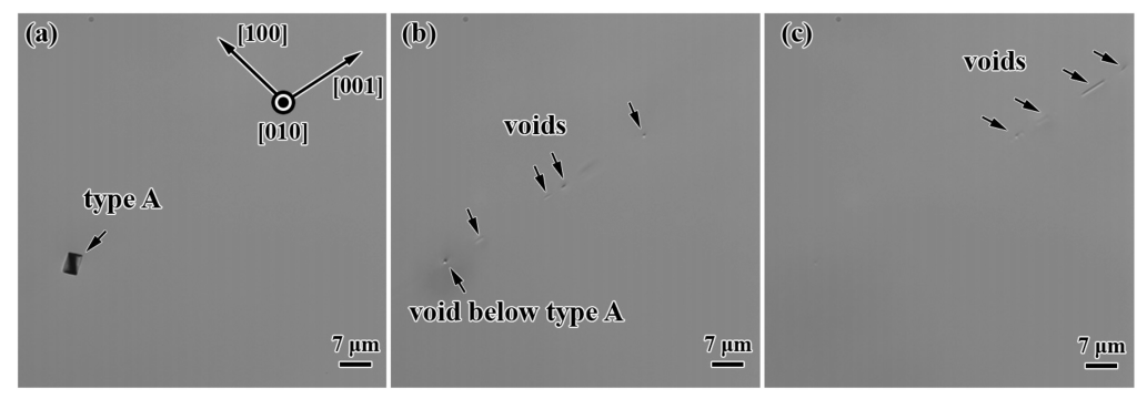
Fig. 9. Discontinuous voids inside the bulk were uncovered by changing the focus depth.(a) Image showing typeA etch pit by focusing on the surface.(b) Discontinuous voids on the (100) plane along [001] direction inside the sample were detected by changing the focus depth.(c) Termination of voids and emerging band such as voids inside the sample by further increasing the focus depth. 50% KOH at130 °C for24 min on the (010) orientated sample.
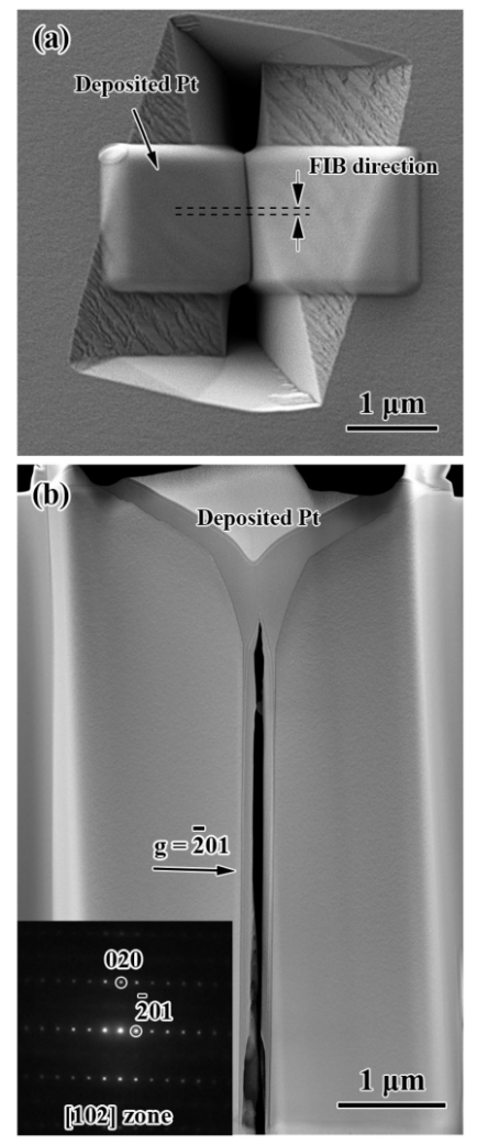
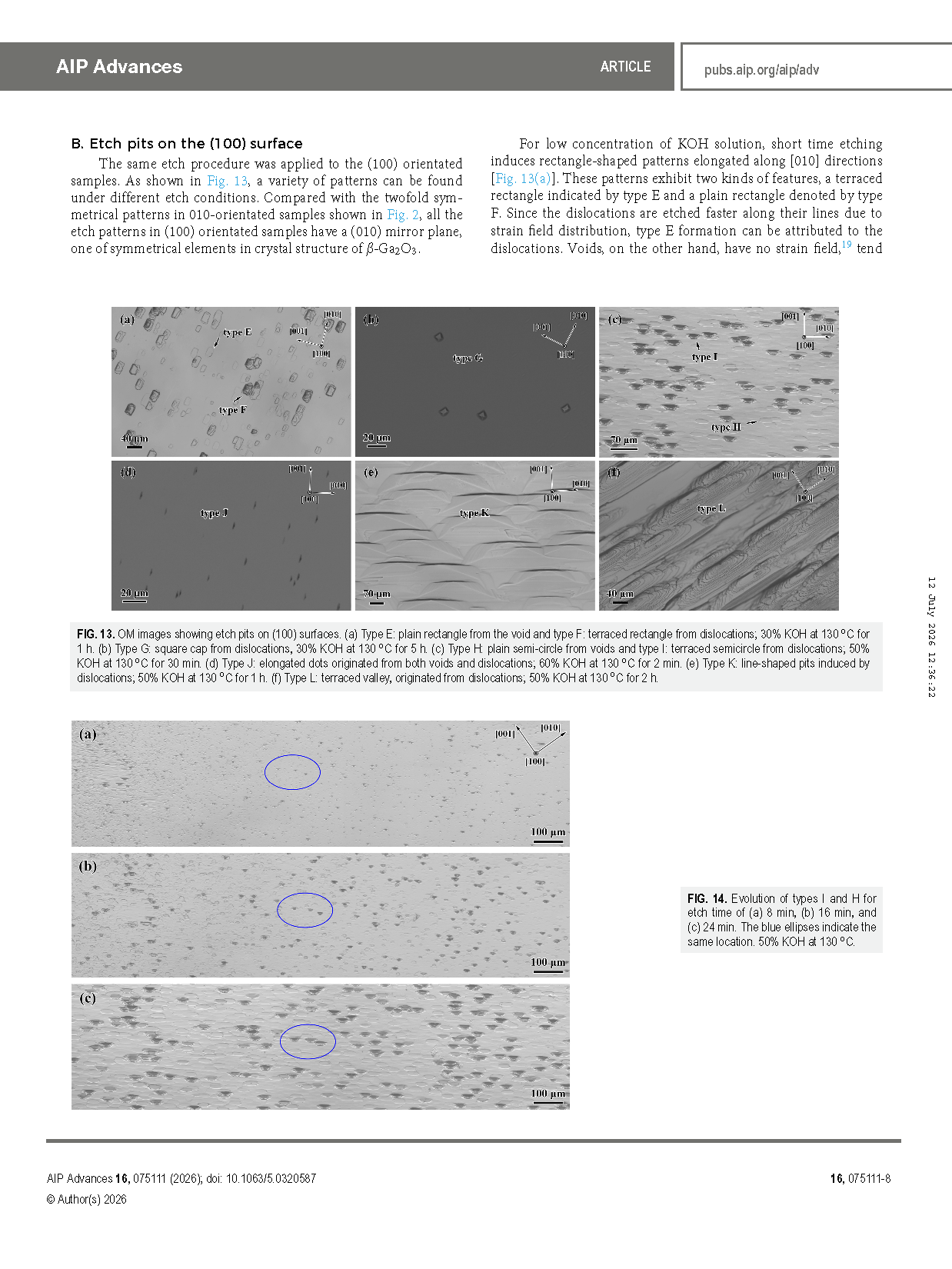
Fig. 10. SEM and TEM images showing the structure of typeA. (a) SEM image showing the location where the TEM sample is prepared by FIB.(b) DFSTEM image showing the slit below typeA.The inset shows the diffraction pattern. 50% KOH at 130 °C for24 min on the (010) orientated sample.
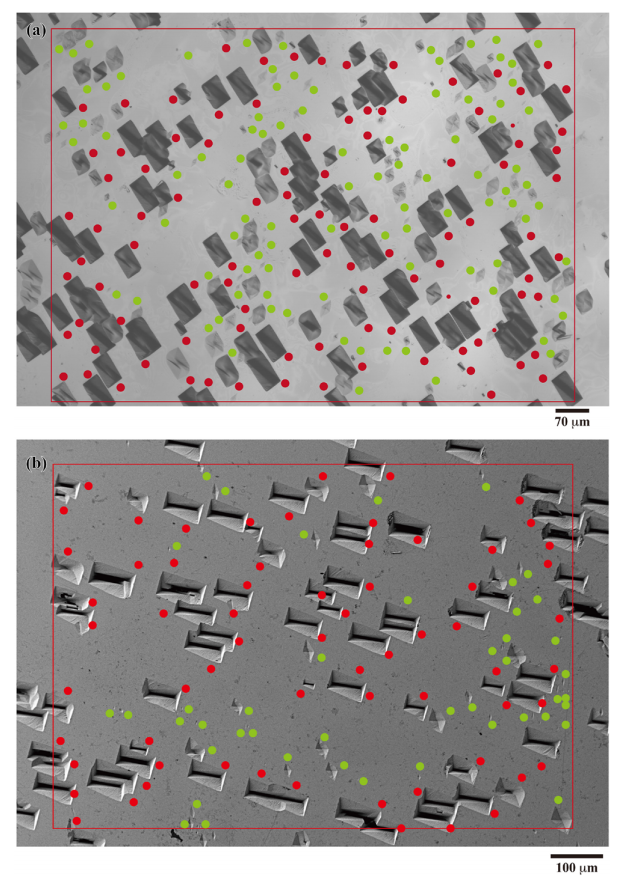
Fig. 11. Etch pit density measurement for the (010) orientated sample. (a) OM image showing density of voids around 1.1 ×10⁴ cm⁻² given by the numbers of typeA divided by the area indicated by the red rectangle and dislocations around 1.1 ×10⁴ cm⁻² are given by the numbers of typesB and C divided by the area.(b) SEMimage showing the void density of 1 ×10⁴ cm⁻² and dislocations of 7 ×10³ cm⁻². The red circles indicate the voids and the green circles indicate dislocations. The red rectangles are the area where etch pits are counted.
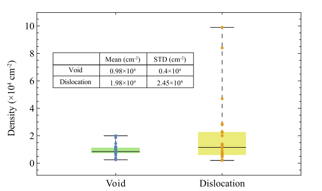
Fig. 12. Boxplot of void and dislocation density from (010) oriented samples.
DOI :
10.1063/5.0320587
Instruction
Official Account

Cooperation
Top
