



A research team led by Professors Qingwen Song and Yuming Zhang from Xidian University, in collaboration with Professor Lianbi Li from Xi’an Polytechnic University and Professor Jichao Hu from Xi’an University of Technology, published an article in Chemical Engineering Journal entitled “Surface-Step-Controlled In-Plane Orientation of β-Ga2O3 Films on 4H-SiC for Deep-Ultraviolet Photodetectors”.
Background
Gallium oxide (Ga2O3), an ultra-wide-bandgap semiconductor with a bandgap of approximately 4.8 eV, has attracted considerable interest for power electronics, deep-ultraviolet (DUV) optoelectronics, and harsh-environment sensing. Its intrinsic solar-blind response makes β-Ga2O3 particularly attractive for DUV photodetection without additional optical filters. However, operation at elevated temperatures is often accompanied by increased dark current and degraded signal-to-noise-related performance. Therefore, high-quality β-Ga2O3 films with controlled crystallographic orientation and reliable high-temperature photoresponse are essential for advancing DUV photodetectors.
Heteroepitaxy provides greater flexibility than growth on native β-Ga2O3 substrates, and 4H-SiC is a promising platform because of its chemical stability, favorable crystallographic matching, and high thermal conductivity. Although the out-of-plane relationship β-Ga2O3 (-201) ∥ 4H-SiC (0001) can be established, the threefold rotational symmetry of the 4H-SiC (0001) surface and the monoclinic structure of β-Ga2O3 allow six possible in-plane rotational variants. Their coexistence can lead to multidomain growth, local misorientation, and degraded material quality. Suppressing these competing variants and promoting a dominant in-plane orientation therefore remain key challenges for β-Ga2O3/4H-SiC heteroepitaxy.
Abstract
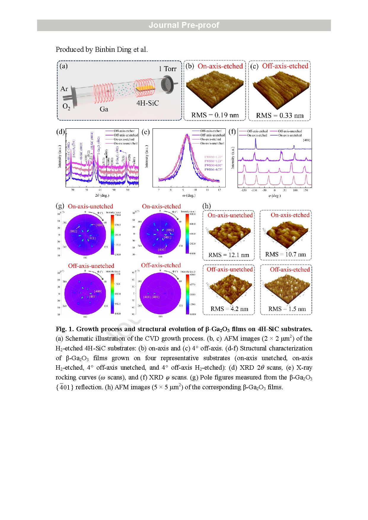
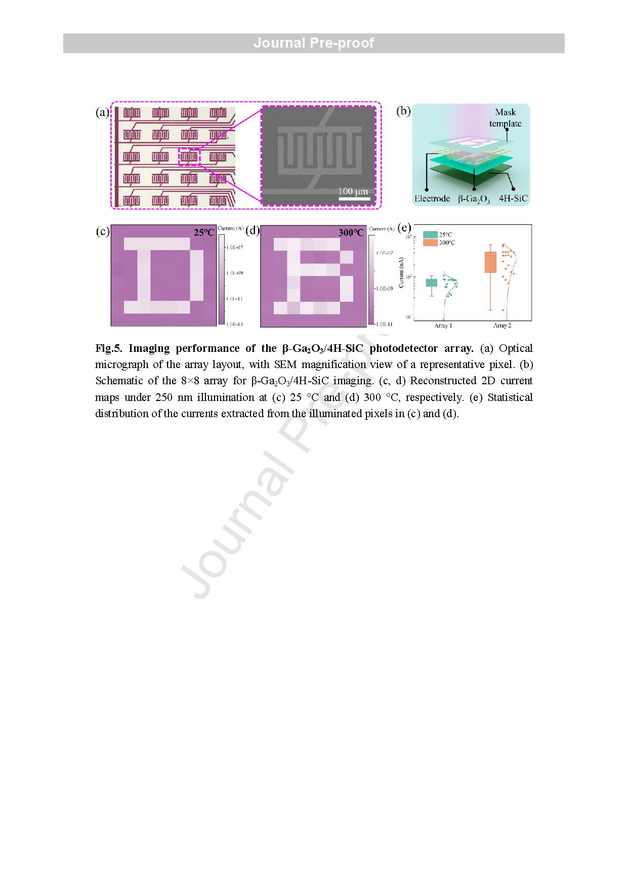
This study addresses the formation of multiple in-plane rotational variants during β-Ga2O3 heteroepitaxy on 4H-SiC and systematically investigates the effects of substrate off-cut and H₂-induced surface steps on the orientation evolution of the films. β-Ga2O3 films were grown on surface-treated 4H-SiC substrates by chemical vapor deposition (CVD), and the effect of substrate off-cut and H2-induced surface steps on the crystallographic orientation evolution was systematically investigated. By comparing on-axis and 4° off-axis 4H-SiC substrates with and without H2 etching, together with XRD φ-scan and pole figure measurements, we show that the stepped off-axis surface strongly suppresses competing in-plane rotational variants and promotes the formation of a dominant β-Ga2O3 orientation. Density functional theory calculations were used to understand the preferential bonding between β-Ga2O3 (-201) and 4H-SiC (0001), providing theoretical support for the observed epitaxial alignment. Based on the optimized films, lateral Pt/β-Ga2O3/Pt MSM photodetectors were fabricated, showing a distinguishable DUV photoresponse at 300 °C despite increased dark current at high temperature. An 8 × 8 photodetector array was further demonstrated as a proof-of-concept DUV imaging device. This work provides insight into surface-step-controlled β-Ga2O3 heteroepitaxy on 4H-SiC and its application potential for high-temperature DUV imaging and sensing applications.
Highlights
A four-group comparison using on-axis and off-axis 4H-SiC substrates with and without H₂ etching was established to systematically reveal the role of surface steps in controlling the in-plane orientation of β-Ga2O3.
Surface steps were used to regulate the in-plane nucleation orientation of β-Ga2O3, effectively suppressing competing rotational variants during β-Ga2O3/4H-SiC heteroepitaxy.
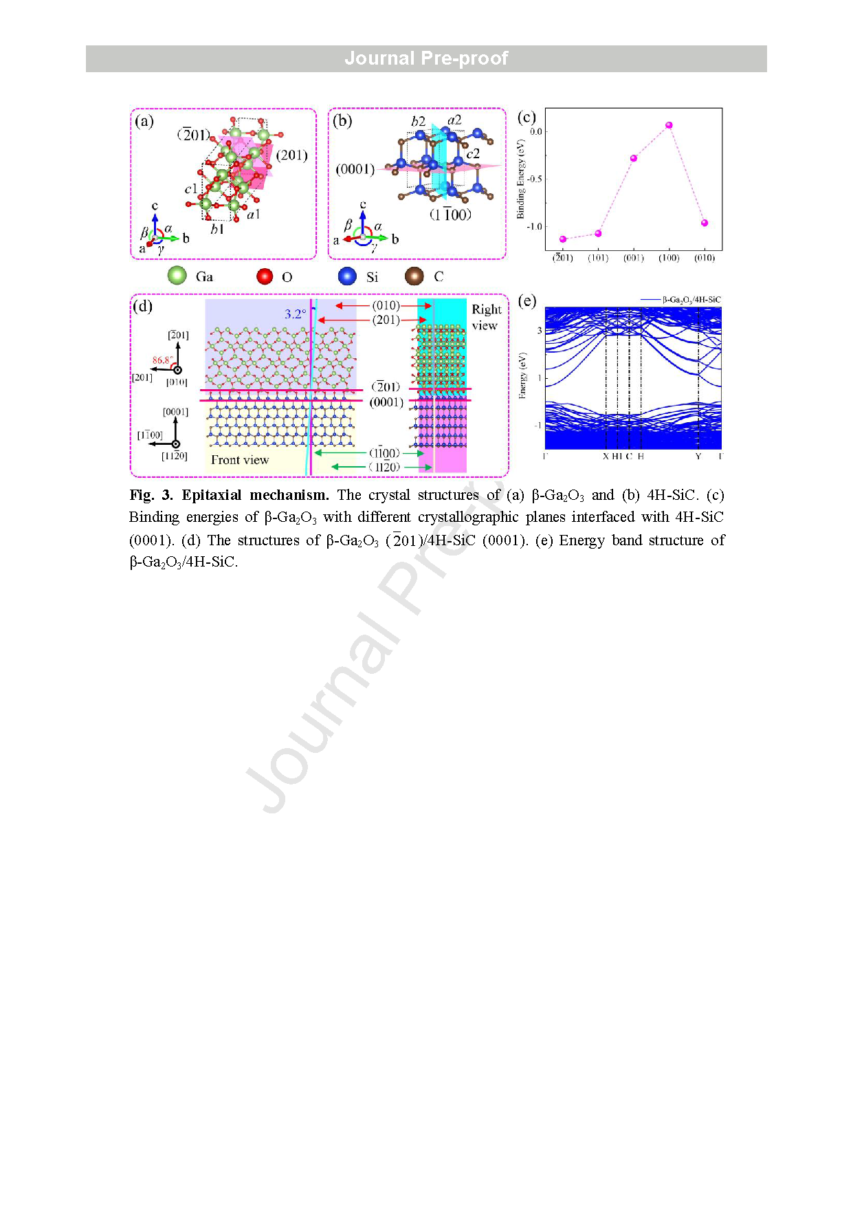
Structural characterization and density functional theory calculations clarified the epitaxial arrangement of β-Ga2O3(-201) ∥4H-SiC (0001) and β-Ga2O3 [010] ∥ 4H-SiC [11-20].
An 8 × 8 array fabricated from the optimized β-Ga2O3/4H-SiC film demonstrated proof-of-concept DUV imaging, supporting the feasibility of this material platform for high-temperature array photodetection.
Conclusion
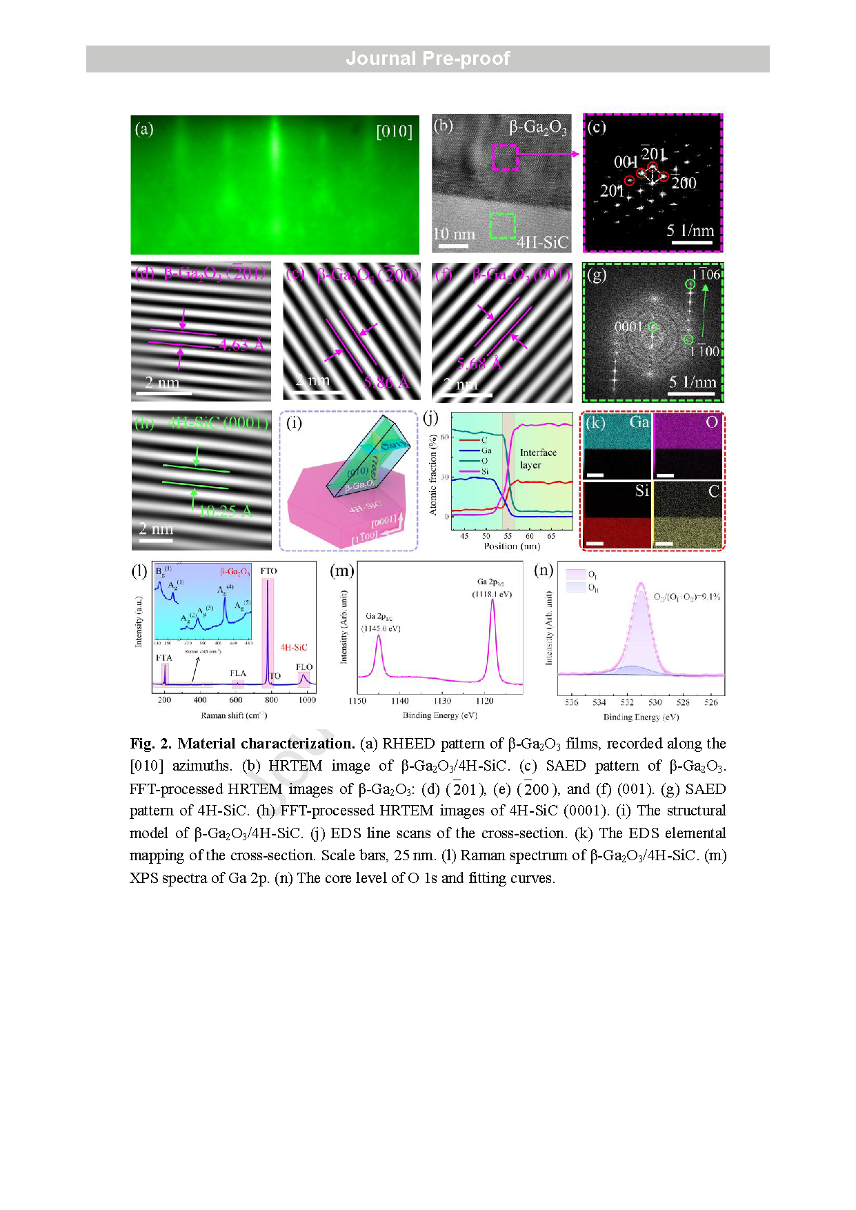
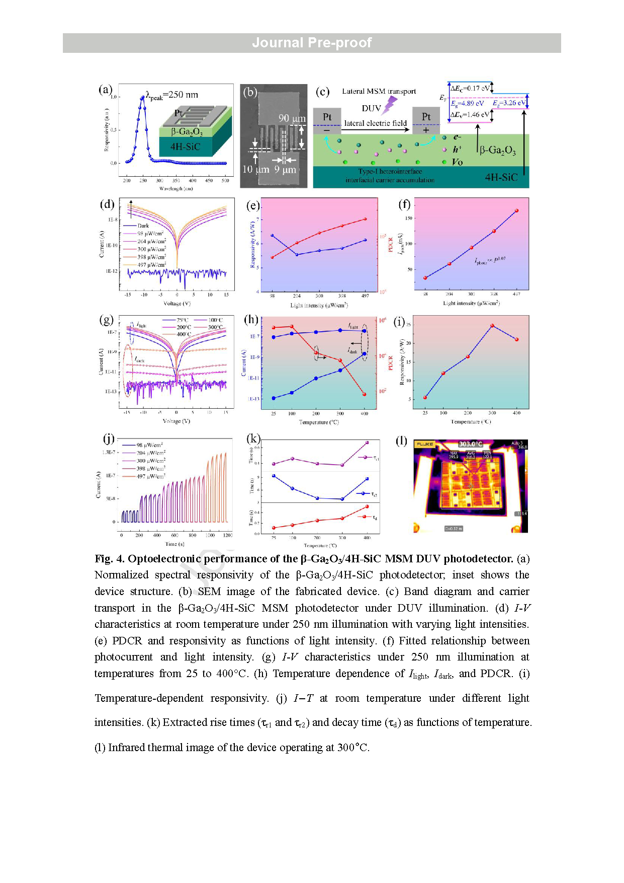
Here, β-Ga2O3 films were grown on 4H-SiC substrates by CVD, and the effects of substrate off-cut and H2-induced surface steps on the in-plane orientation were systematically investigated. Cross-comparison experiments using on-axis and 4° off-axis 4H-SiC substrates with and without H2 etching show that the stepped off-axis surface effectively suppresses competing rotational variants. XRD φ-scan and pole figure measurements reveal a transition from six in-plane variants to a dominant orientation with minor 180° rotational variants. As a result, the rocking-curve FWHM decreases from 1.26° to 0.75°, and the RMS roughness is reduced from 12.1 to 1.5 nm. Structural and DFT analyses confirm β-Ga2O3 (-201) ∥ 4H-SiC (0001) and β-Ga2O3 [010] ∥ 4H-SiC [11-20], with a favorable binding energy of -1.13 eV. The optimized film shows an OII/(OI + OII) ratio of 9.1%. Based on this film, lateral MSM DUV photodetectors exhibit a distinguishable photoresponse at 300 °C, achieving a PDCR of ~5 × 10³ and a responsivity of 24.79 A/W. and an 8 × 8 array demonstrates proof-of-concept DUV imaging.
Project Support
This work was supported in part by, the National Natural Science Foundation of China under Grant 62404163 and U2330109, the China Postdoctoral Science Foundation under Grant 2024M752516, Key Research and Development Program of Shaanxi Province under Grant 2025GH-YBXM-052 and 2024GX-YBXM-081), Basic Research Program of Natural Science of Shaanxi Province under Grant 2025JC-YBQN-759 and 2024JC-YBMS-023, Shaanxi Province "Scientist + Engineer" Team Building under Grant 2025QCY-KXJ-041), Science and Technology Plan Project of Xi’an under Grant 25GXKJRC00074.

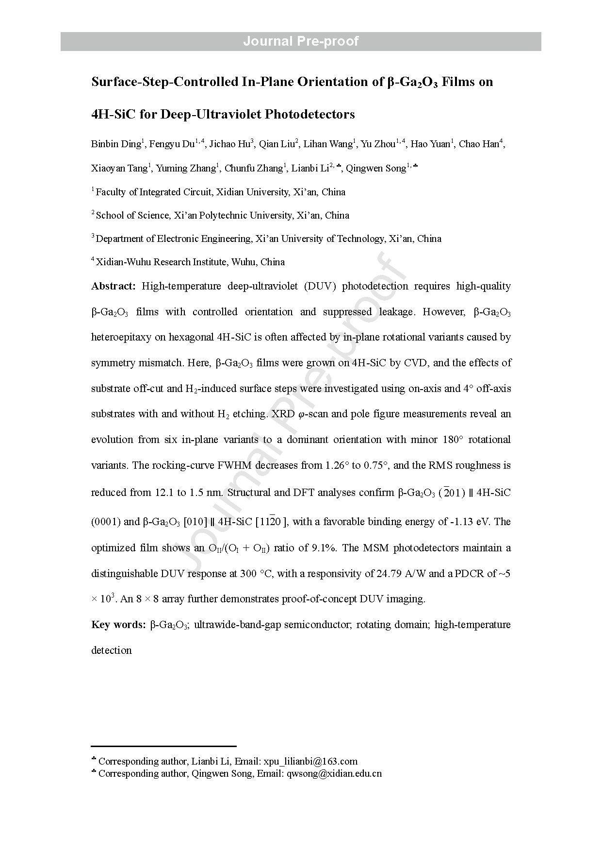
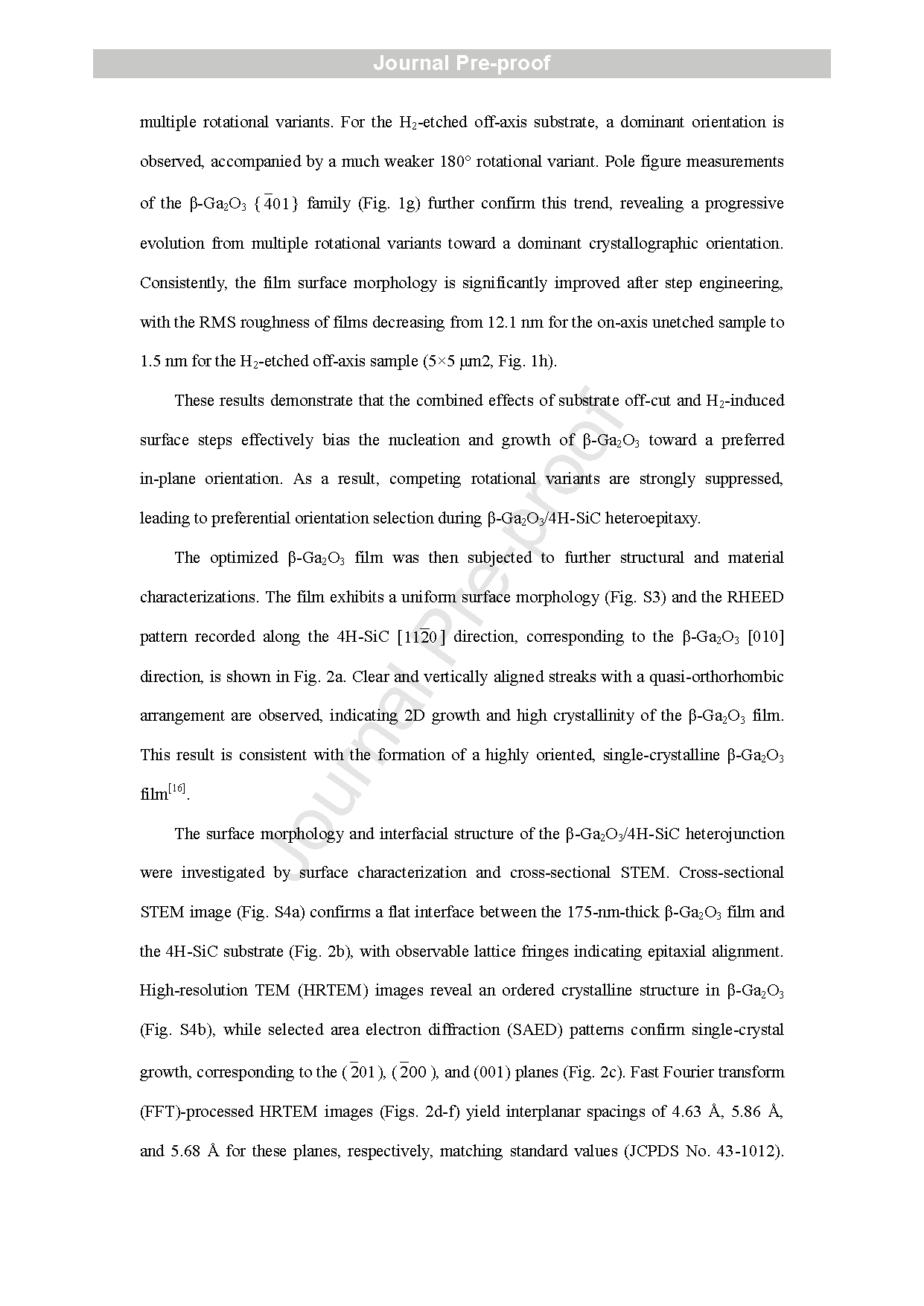
Fig. 1. Growth process and structural evolution of β-Ga2O3 films on 4H-SiC substrates. (a) Schematic illustration of the CVD growth process. (b, c) AFM images (2 × 2 μm2) of the H2-etched 4H-SiC substrates: (b) on-axis and (c) 4° off-axis. (d-f) Structural characterization of β-Ga2O3 films grown on four representative substrates (on-axis unetched, on-axis H2-etched, 4° off-axis unetched, and 4° off-axis H2-etched): (d) XRD 2θ scans, (e) X-ray rocking curves (ω scans), and (f) XRD φ scans. (g) Pole figures measured from the β-Ga2O3 {-401} reflection. (h) AFM images (5 × 5 μm2) of the corresponding β-Ga2O3 films.
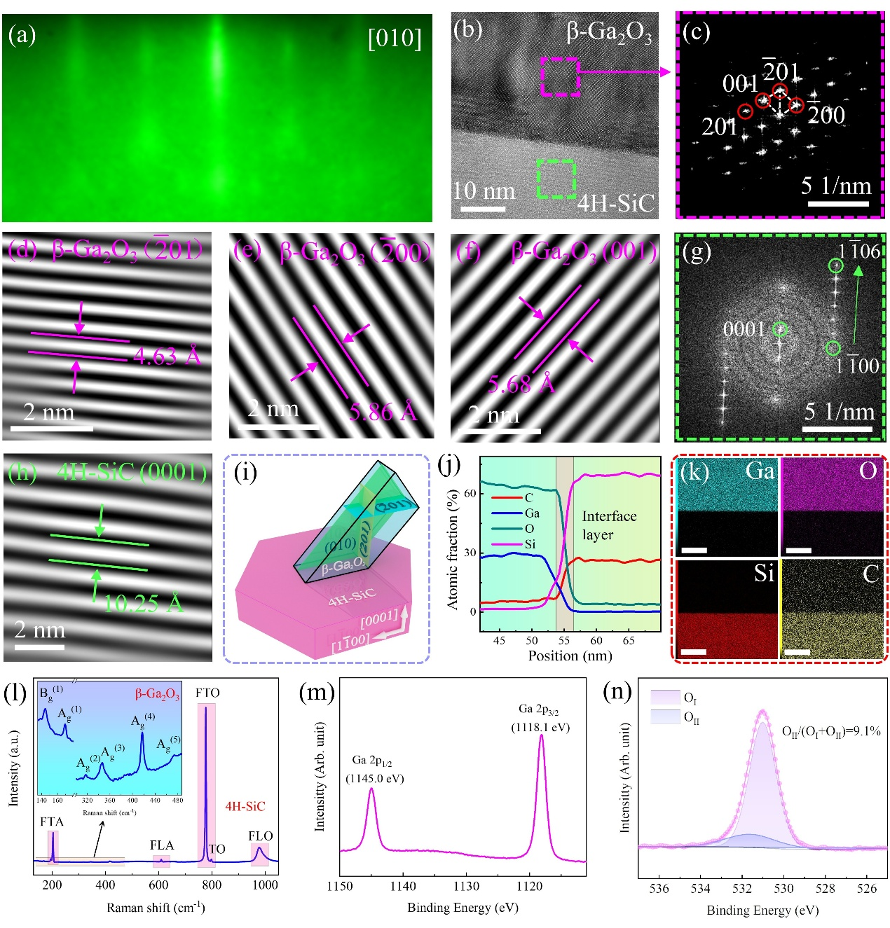
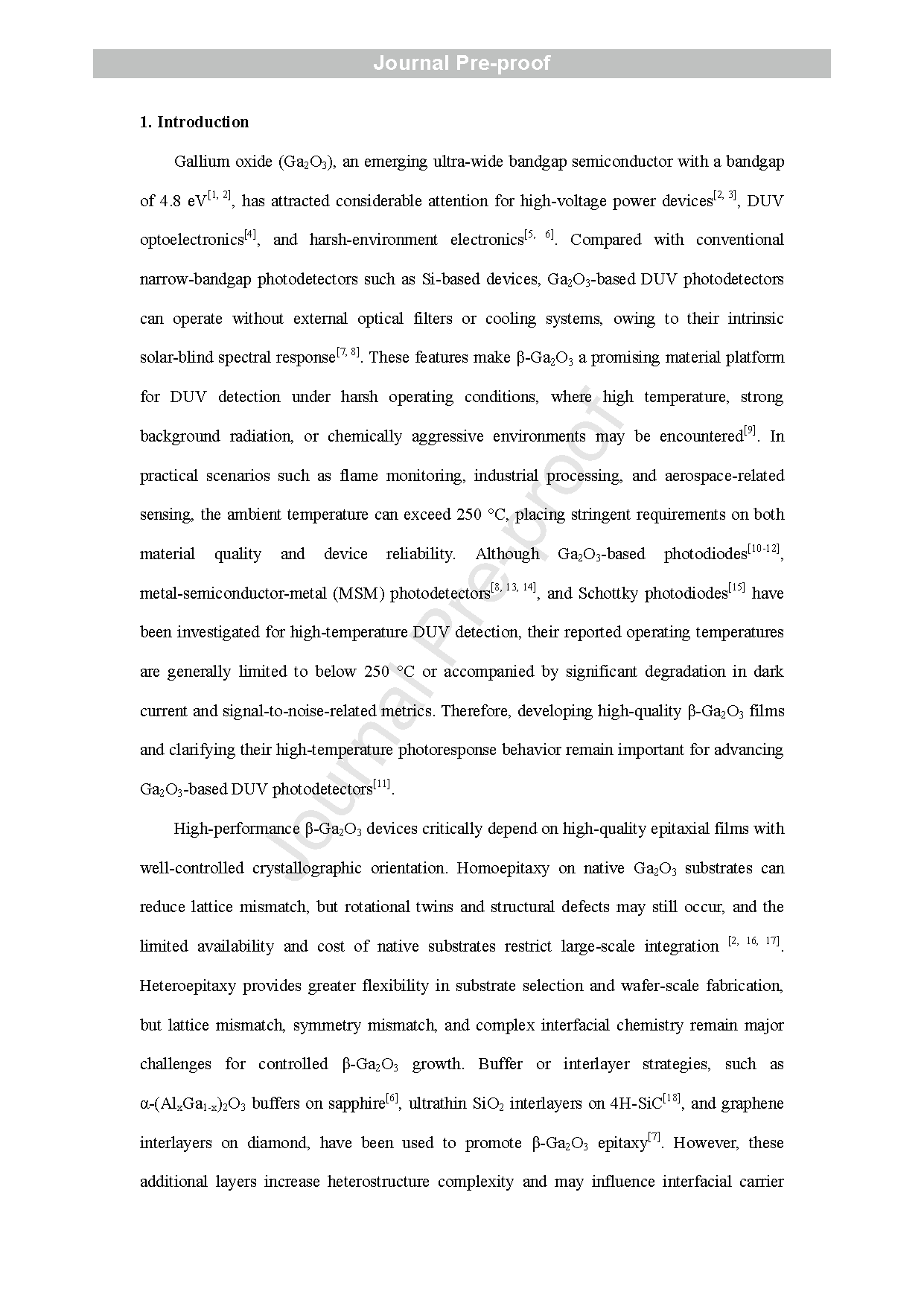
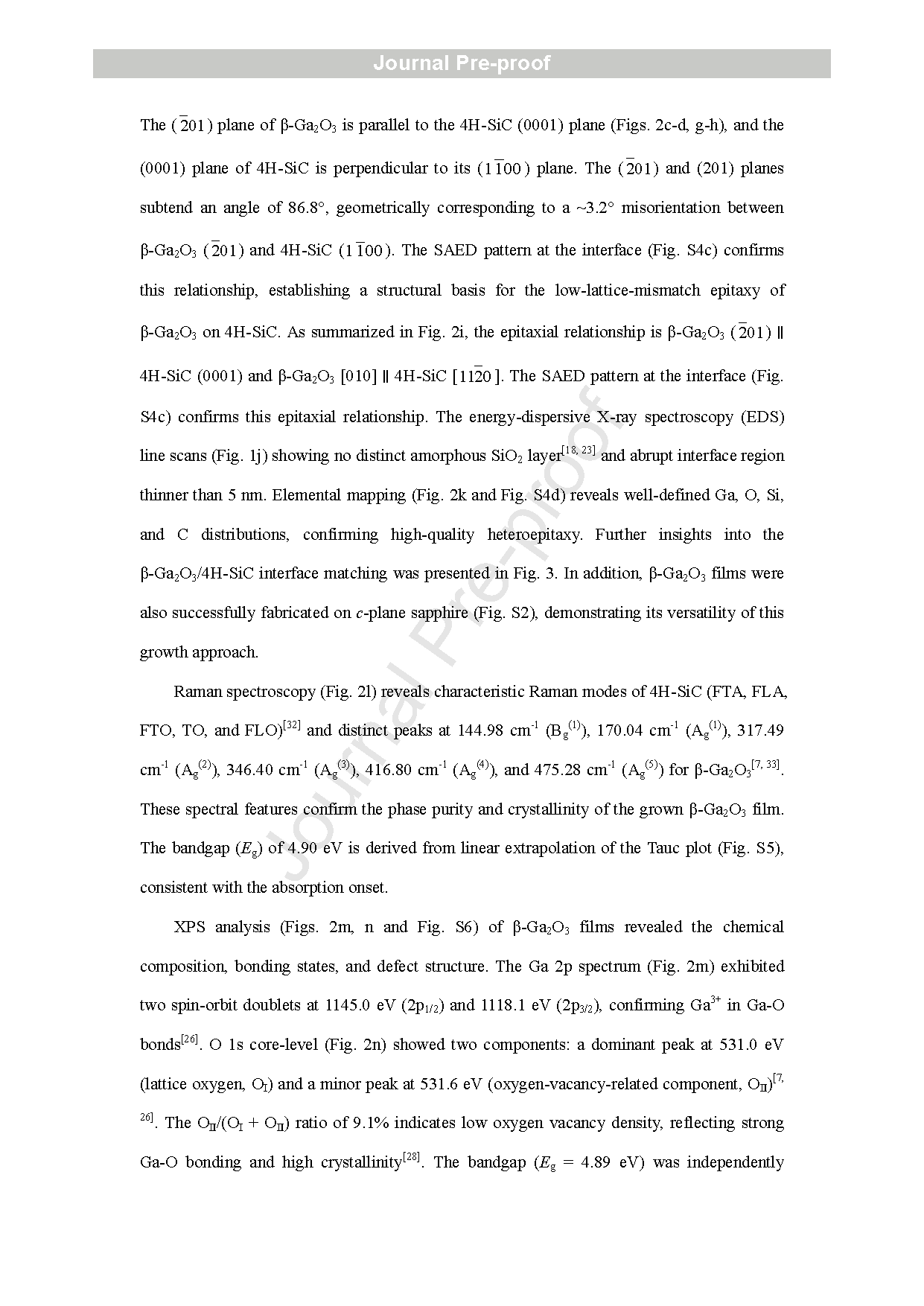
Fig. 2. Material characterization. (a) RHEED pattern of β-Ga2O3 films, recorded along the [010] azimuths. (b) HRTEM image of β-Ga2O3/4H-SiC. (c) SAED pattern of β-Ga2O3. FFT-processed HRTEM images of β-Ga2O3: (d) (-201), (e) (-200), and (f) (001). (g) SAED pattern of 4H-SiC. (h) FFT-processed HRTEM images of 4H-SiC (0001). (i) The structural model of β-Ga2O3/4H-SiC. (j) EDS line scans of the cross-section. (k) The EDS elemental mapping of the cross-section. Scale bars, 25 nm. (l) Raman spectrum of β-Ga2O3/4H-SiC. (m) XPS spectra of Ga 2p. (n) The core level of O 1s and fitting curves.
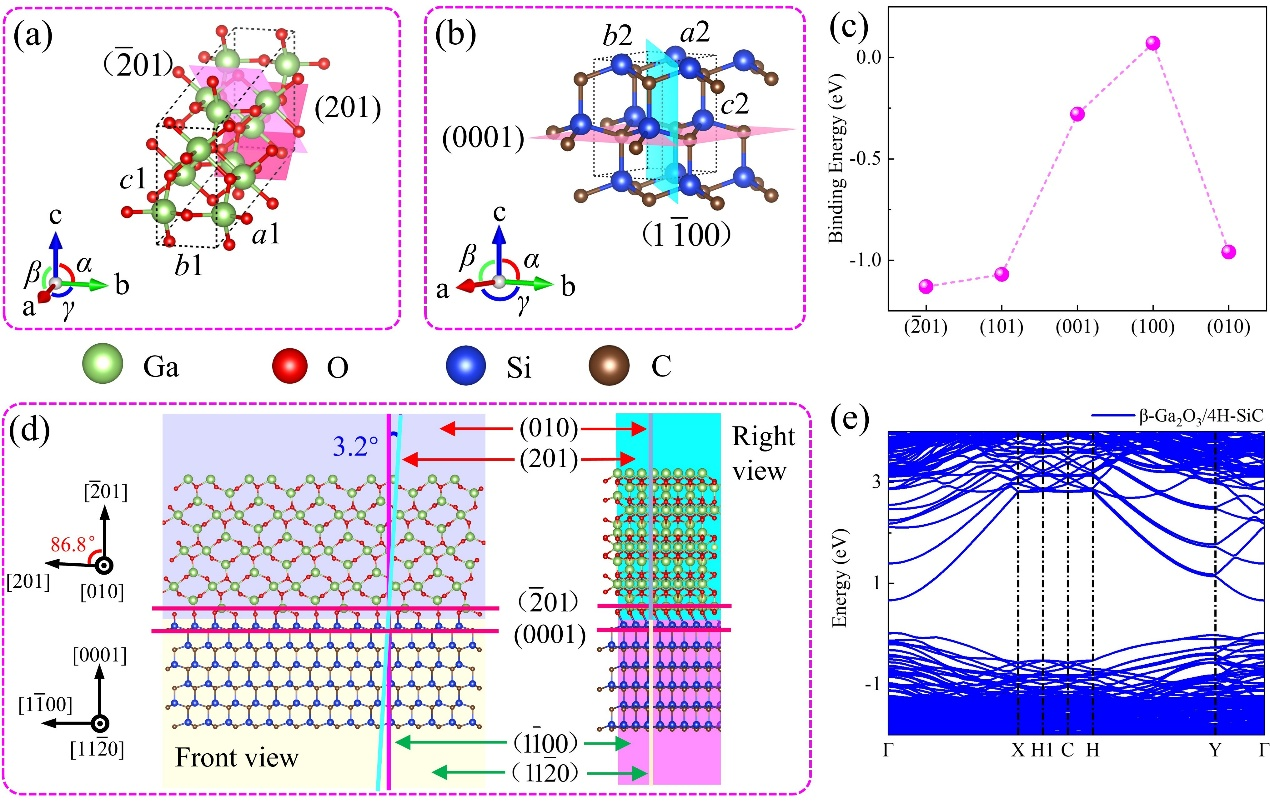
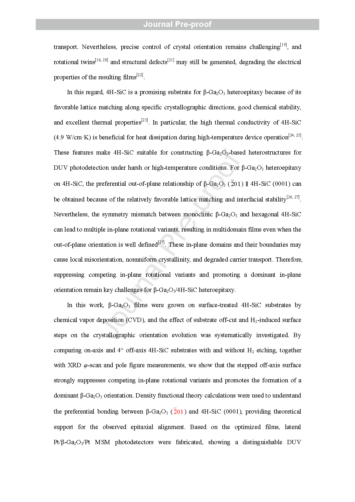
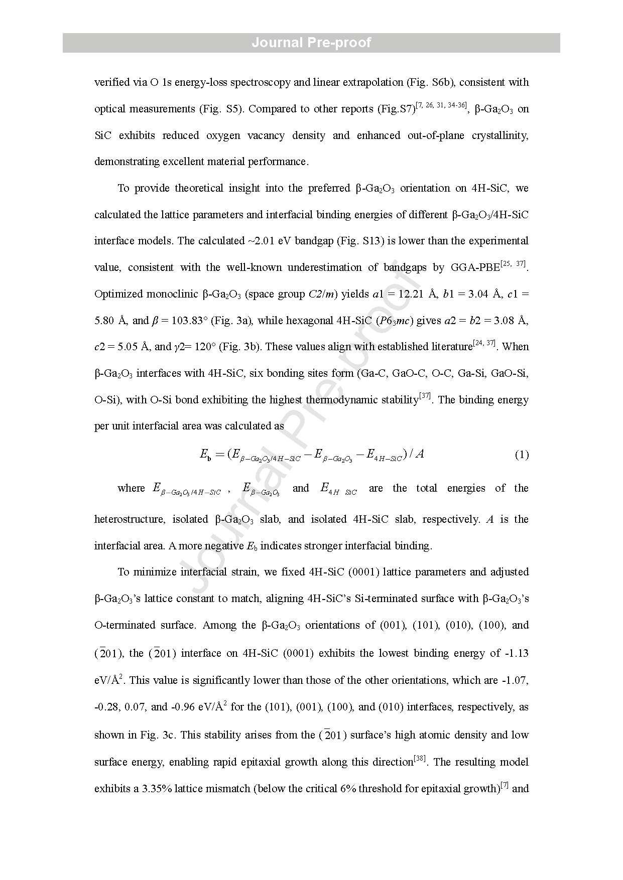
Fig. 3. Epitaxial mechanism. The crystal structures of (a) β-Ga2O3 and (b) 4H-SiC. (c) Binding energies of β-Ga2O3 with different crystallographic planes interfaced with 4H-SiC (0001). (d) The structures of β-Ga2O3 (-201)/4H-SiC (0001). (e) Energy band structure of β-Ga2O3/4H-SiC.
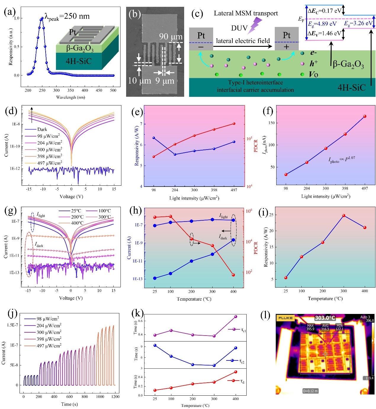
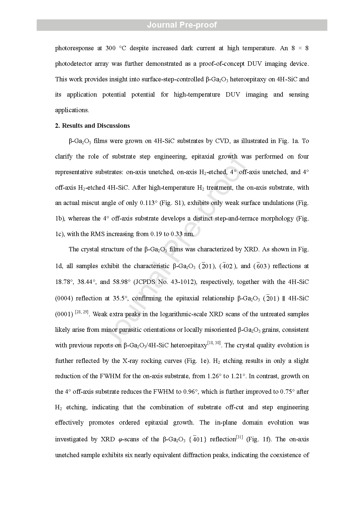
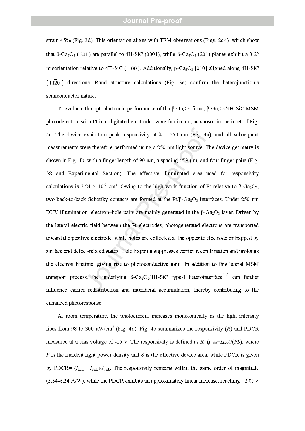
Fig. 4. Optoelectronic performance of the β-Ga2O3/4H-SiC MSM DUV photodetector. (a) Normalized spectral responsivity of the β-Ga2O3/4H-SiC photodetector; inset shows the device structure. (b) SEM image of the fabricated device. (c) Band diagram and carrier transport in the β-Ga2O3/4H-SiC MSM photodetector under DUV illumination. (d) I-V characteristics at room temperature under 250 nm illumination with varying light intensities. (e) PDCR and responsivity as functions of light intensity. (f) Fitted relationship between photocurrent and light intensity. (g) I-V characteristics under 250 nm illumination at temperatures from 25 to 400°C. (h) Temperature dependence of Ilight, Idark, and PDCR. (i) Temperature-dependent responsivity. (j) I–T at room temperature under different light intensities. (k) Extracted rise times (τr1 and τr2) and decay time (τd) as functions of temperature. (l) Infrared thermal image of the device operating at 300°C.
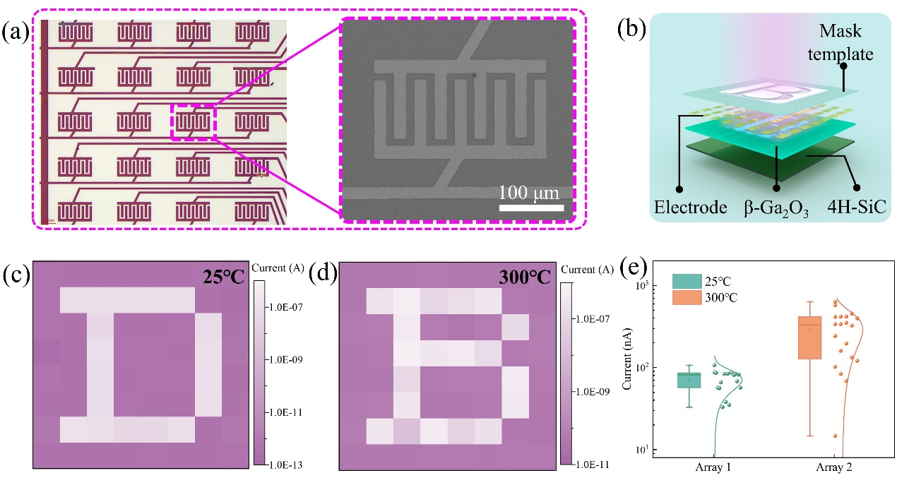
Fig.5. Imaging performance of the β-Ga2O3/4H-SiC photodetector array. (a) Optical micrograph of the array layout, with SEM magnification view of a representative pixel. (b) Schematic of the 8×8 array for β-Ga2O3/4H-SiC imaging. (c, d) Reconstructed 2D current maps under 250 nm illumination at (c) 25 °C and (d) 300 °C, respectively. (e) Statistical distribution of the currents extracted from the illuminated pixels in (c) and (d).
DOI:
doi.org/10.1016/j.cej.2026.179684



Instruction
Official Account

Cooperation
Top
