


Researchers from BITS Pilani, IIT Guwahati have published a dissertation titled " Two-dimensional electron gas at Ga₂O₃ heterojunctions: Progress, challenges, and future prospects " in Applied Physics Reviews.
Background
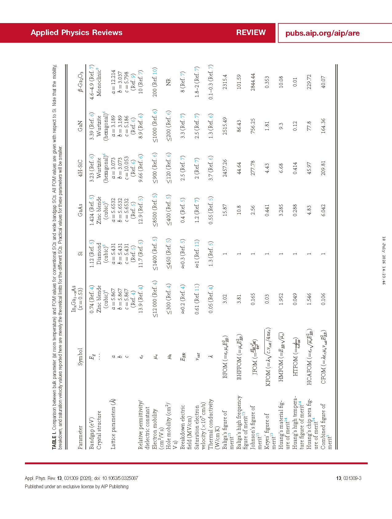
The power semiconductor industry is vigorously developing wide-bandgap semiconductor technologies to exploit outstanding electrical properties such as ultrahigh breakdown electric field, and gallium oxide (Ga₂O₃) has become a key research material. Ga₂O₃ is a polymorphic ultra-wide bandgap semiconductor with a bandgap of 4.6–4.9 eV. It features extreme breakdown field strength and relatively high electron saturation velocity, and its power and radio frequency (RF) figures of merit outperform silicon, SiC and GaN, making it an ideal candidate for next-generation high-power RF power devices. Various Ga₂O₃-based field effect transistors (FETs) have been fabricated, yet intrinsic drawbacks of Ga₂O₃ restrict device performance: low electron mobility, poor thermal conductivity, and the difficulty of p-type doping, so conventional FETs cannot fully unlock the material’s potential.High electron mobility transistors (HEMTs) adopt interfacial two-dimensional electron gas (2DEG) as conductive channels, which isolate dopant impurity scattering and greatly improve effective mobility. Polar heterostructure HEMTs can achieve ultrahigh sheet carrier density to boost current capacity and reduce on-resistance, perfectly matching high-power RF demands. At present, research on interfacial 2DEG and corresponding Ga₂O₃ HEMTs is booming worldwide. However, systematic reviews are scarce in this field. No unified summary covers two 2DEG formation mechanisms (modulation doping and polar heterostructures), nor a full comparison of alloy, III-nitride and phase heterojunctions including simulation and experimental results. Industrial bottlenecks of these devices have not been sorted out, and a clear research roadmap is missing, forming an obvious research gap.
Abstract
In recent times, the semiconductor (SC) power electronics industry has experienced a renewed interest in wide bandgap SCs, with the intent of exploiting their superior performance characteristics, particularly the excellent breakdown fields (EBR). One of the materials at the forefront of these research efforts is gallium sesquioxide or gallium oxide (Ga₂O₃), a polymorphic crystal with a bandgap in the 4.6–4.9 eV range. Ga₂O₃ exhibits high E_BR as a consequence of its wide bandgap and also has a relatively high saturation electron velocity (vsat). Therefore, its figure of merit values are very high, and it is regarded as being highly suitable for use in SC power electronics. Conventional power devices like field effect transistors (FETs) have already been fabricated using Ga₂O₃, exhibiting highly desirable performance, particularly suited to high-power radio frequency (RF) applications. But Ga₂O₃ also has a few disadvantages associated with it, the most pertinent of which are its comparatively low electron mobility (μe), its low thermal conductivity (λ), and the difficulty in achieving p-type doping. Efforts have been made to overcome these issues and realize the full potential of Ga₂O₃-based power electronic devices. Of the Ga₂O₃-based FETs that have been fabricated, high electron mobility transistors (HEMTs) exhibit some of the best performance. These devices utilize two-dimensional electron gas (2DEG) as the conducting channel and generally allow for higher values of effective mobility (μeff) in devices by reducing the impact of dopant scattering on channel electrons. In addition, HEMTs (particularly those based on polar heterostructures) exhibit high values of sheet carrier density (ns), which allows for improved current carrying capacity (ID) and lower on-state resistance (RON), among other benefits. The combined effect of high μeff and ns makes HEMTs very suitable as a high-performance device, especially in the high-power RF application space. As a result, there is a burgeoning interest in the realization of interfacial 2DEG at Ga₂O₃-based heterojunctions and the fabrication of HEMTs based on these junctions. This paper aims to provide some background on the principles governing HEMT technology, summarize research efforts that have so far been made in the fabrication of Ga₂O₃-based HEMTs, discuss where the technology can go in the future and the developments that need to take place for this to happen, and highlight the multitude of challenges preventing further progress. In addition to reviewing the work of others, we have also performed our own simulations on Ga₂O₃-based heterojunctions to further highlight the applicability of these structures. With this work, we hope to spur further advancements in the field of Ga₂O₃-based power electronics and, more specifically, the field of Ga₂O₃-based HEMT technology.
Highlights
Systematically classify and compare three distinct Ga₂O₃heterojunction systems capable of generating 2DEG, including alloy modulation-doped, polymorph polar and III-nitride polar heterostructures.
Elaborate quantitative coupling relationships between band offset, spontaneous polarization, interface defects and 2DE transport properties in all Ga₂O₃heterotype structures.
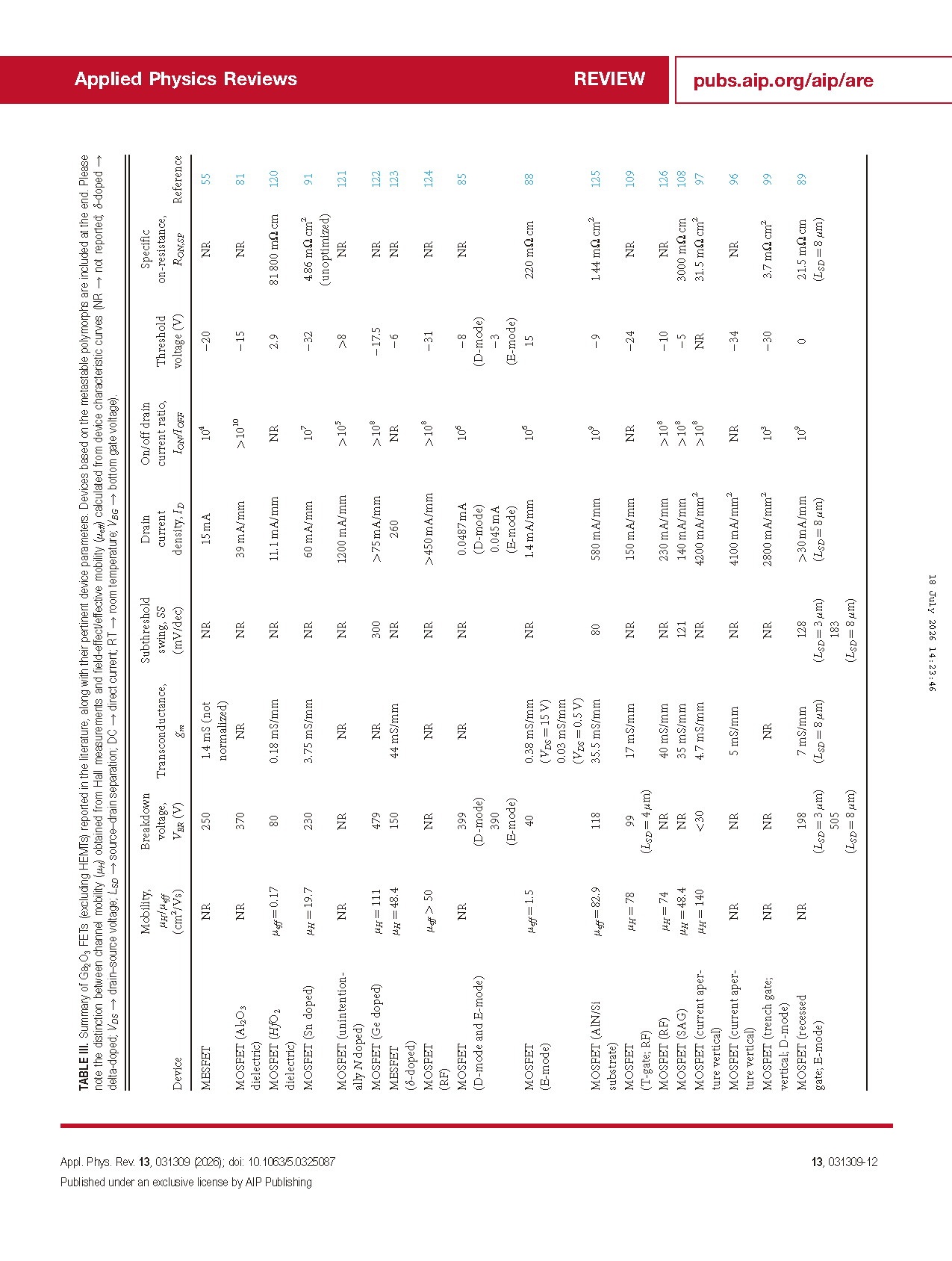
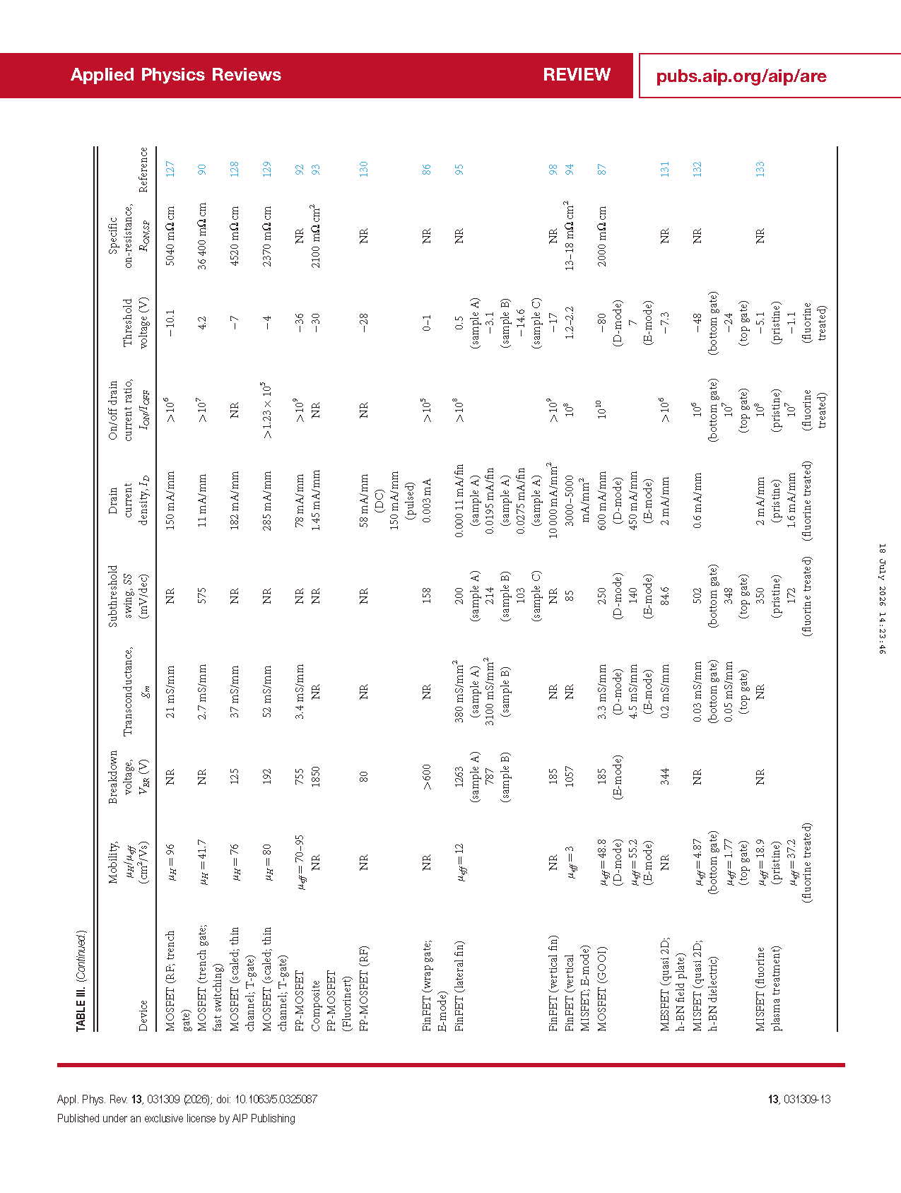
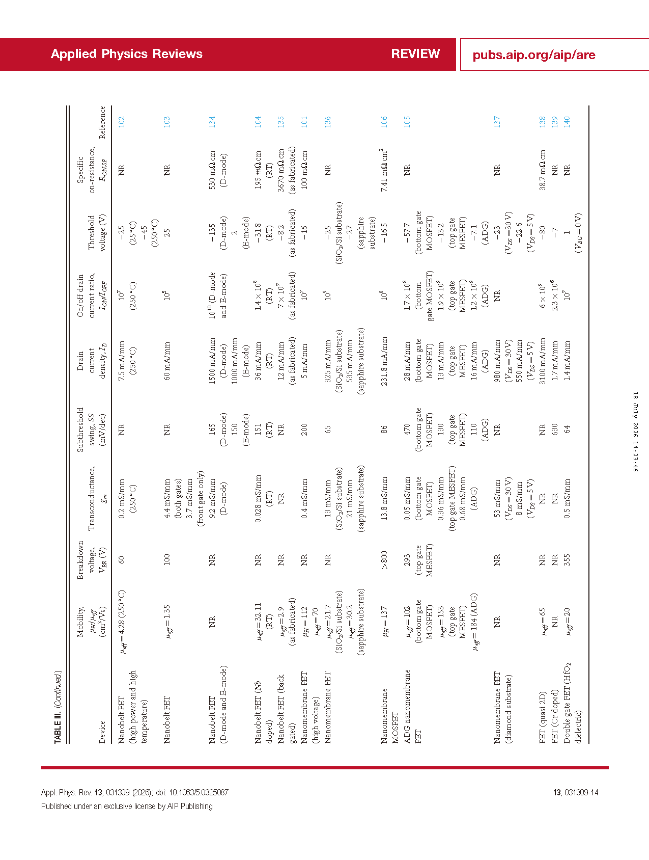
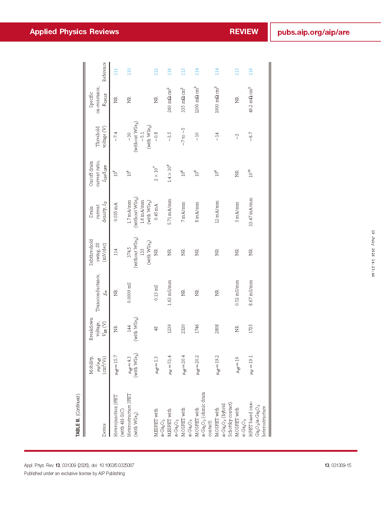
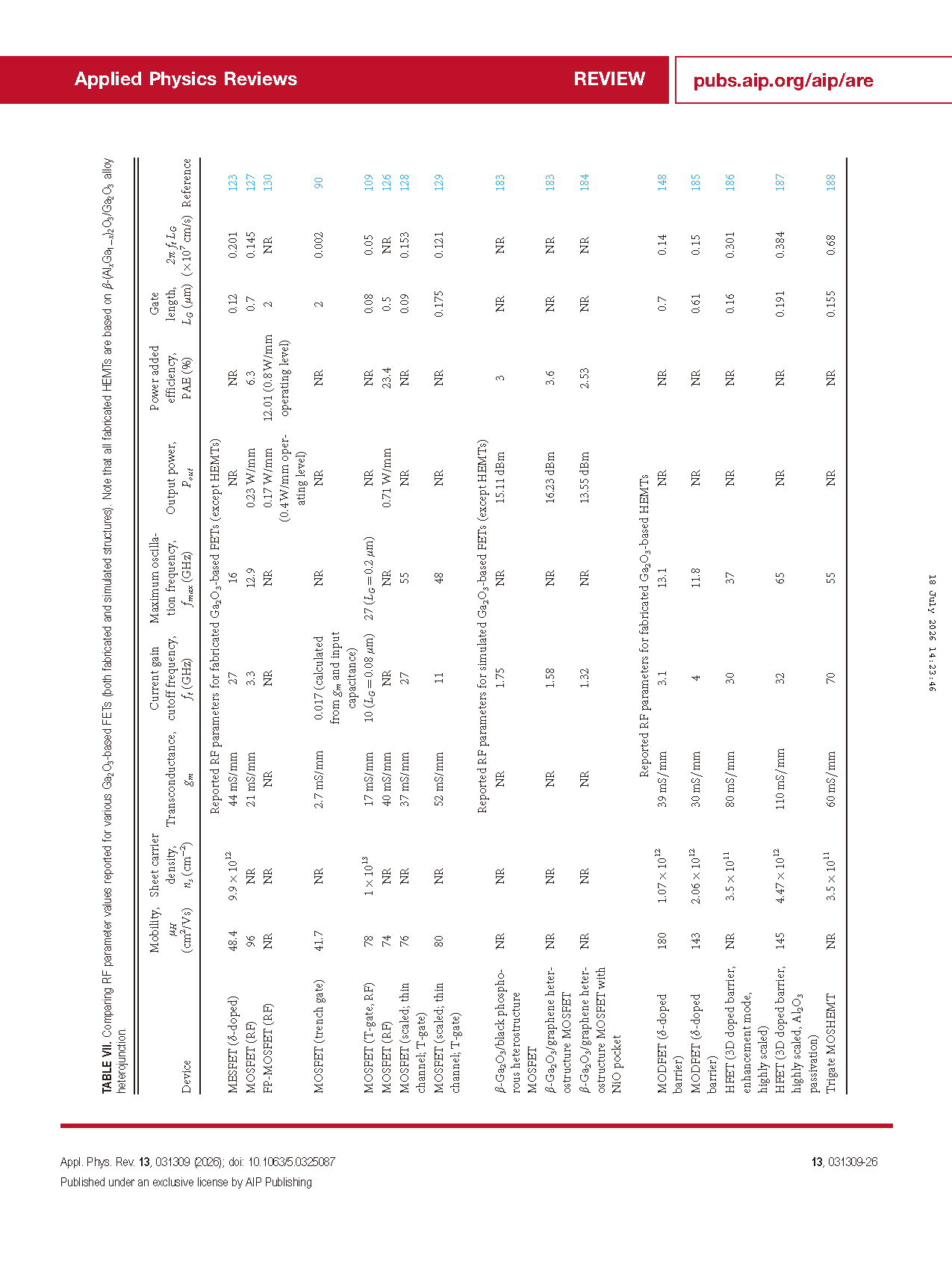
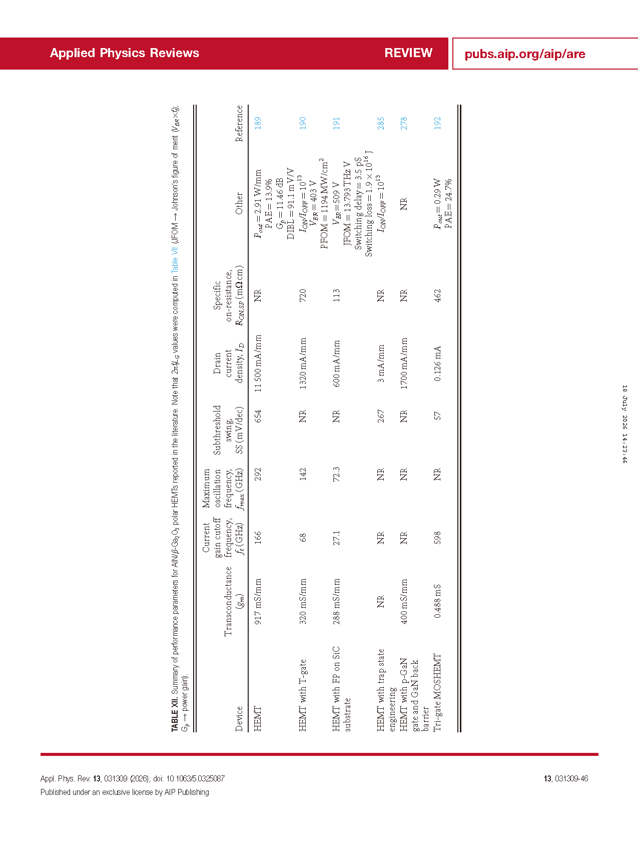
Establish comprehensive performance benchmark table covering mobility, sheet density, breakdown voltage and RF figure of merit for all reported Ga₂O₃HEMTs.
Summarize epitaxial bottlenecks and device reliability issues, and put forward targeted future research schemes for industrialized Ga₂O₃ power/RF HEMTs.
Conclusion
The emergence of wide bandgap SCs has undoubtedly heralded a revolution in SC power electronics. While SiC and GaN were the early standard bearers, the superior FOM values of Ga₂O₃ have made it the new center of attention, and a considerable amount of progress has been made in the field of Ga₂O₃-based electronics over the past decade, particularly in the fabrication of FETs. Ga₂O₃-based HEMTs have the potential to provide device characteristics and performance parameters superior to those of more traditional FETs such as MOSFETs, and their qualities are perfectly attuned to the requirements of modern power devices, particularly with relation to high-power RF applications. This review was compiled with the explicit purpose of providing readers insight into both established and emerging Ga₂O₃-based HEMT technologies.
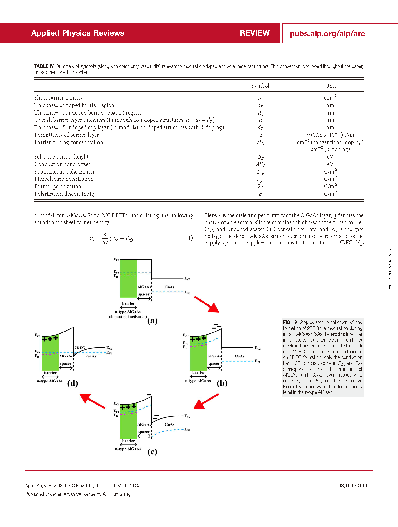
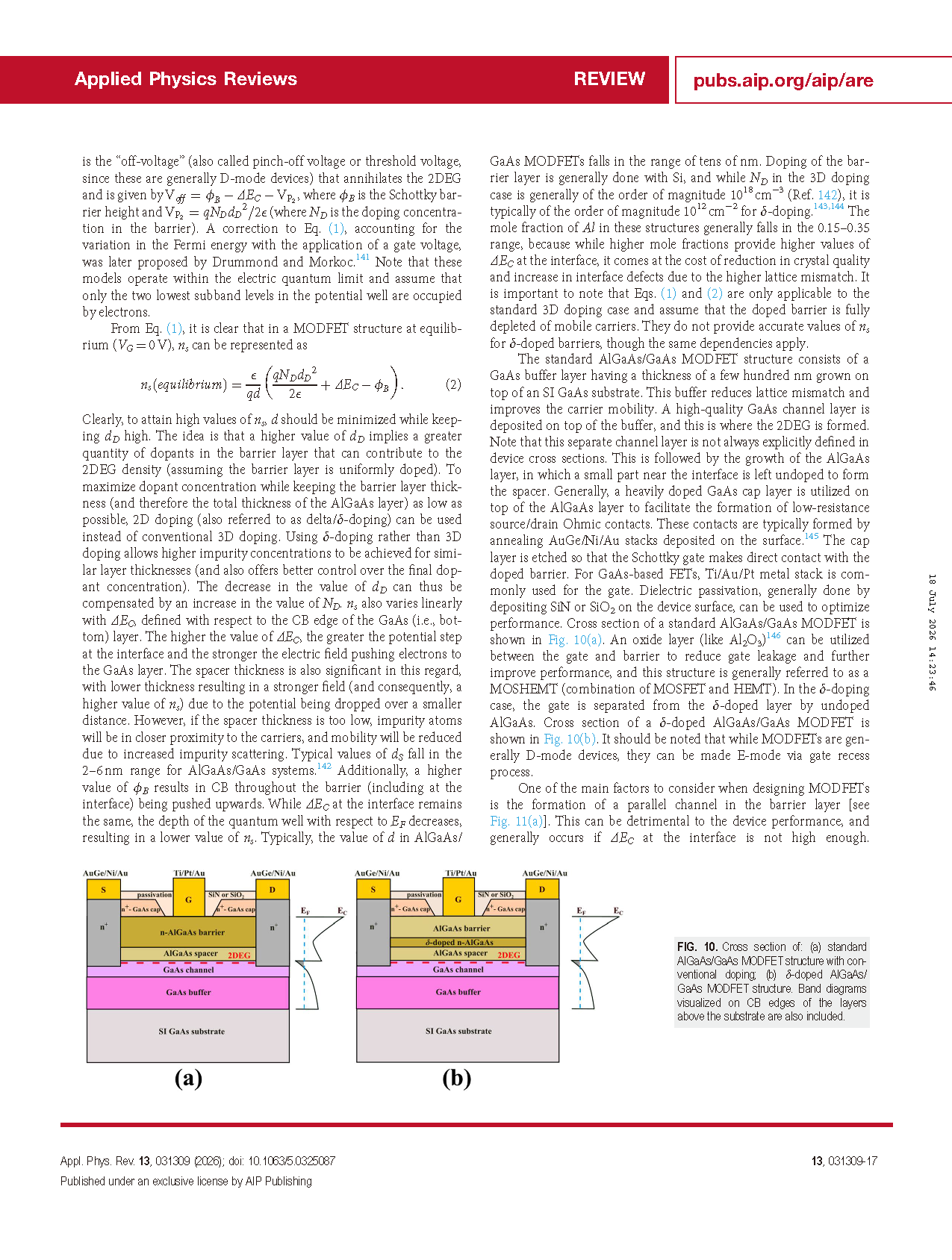
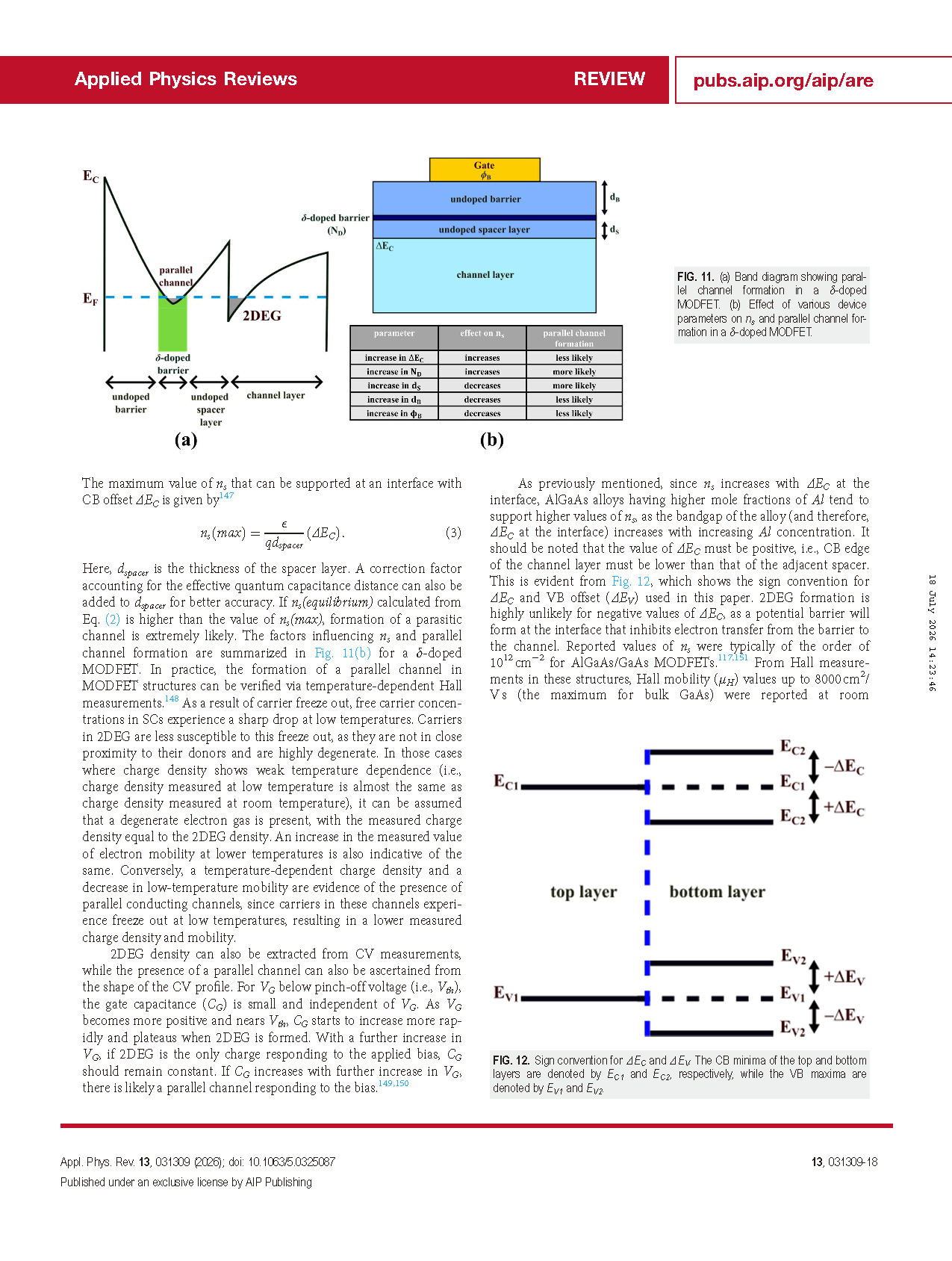
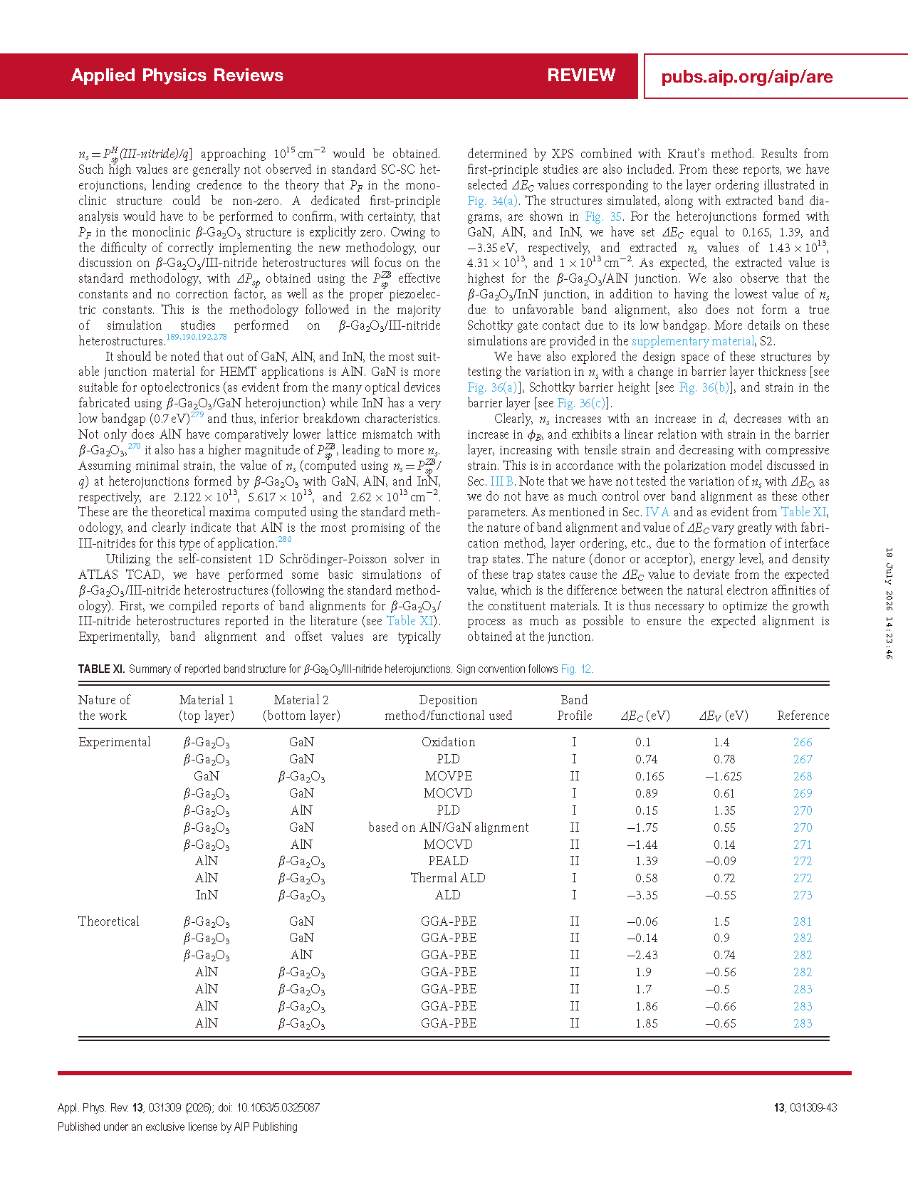
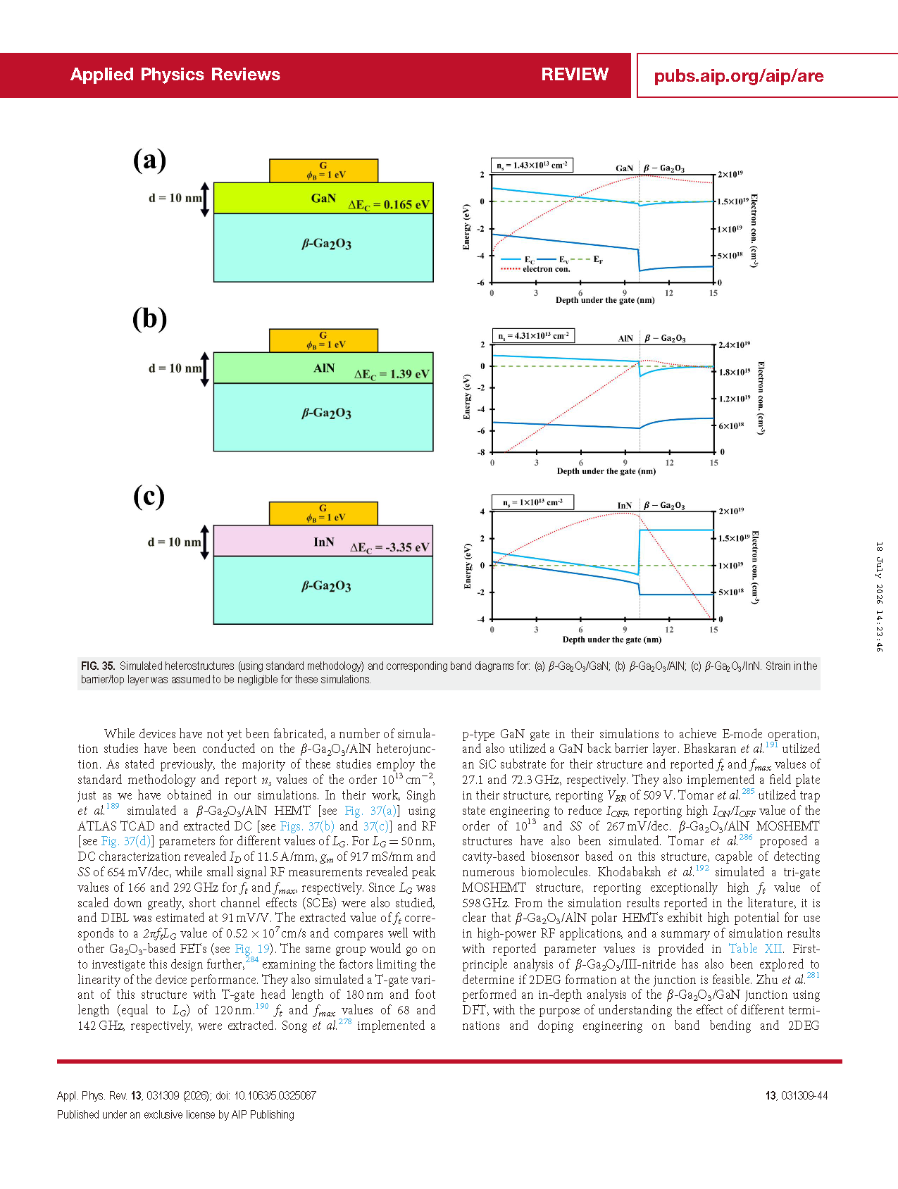
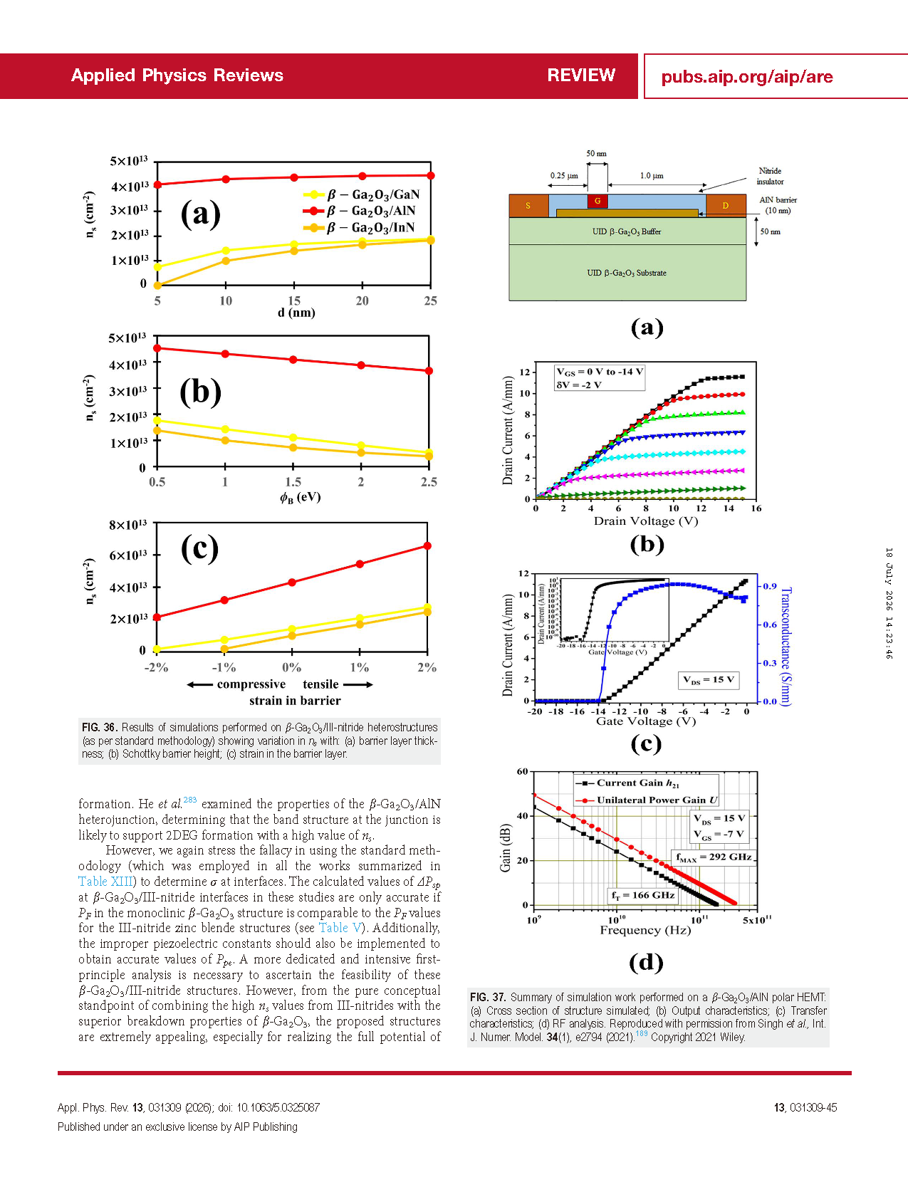
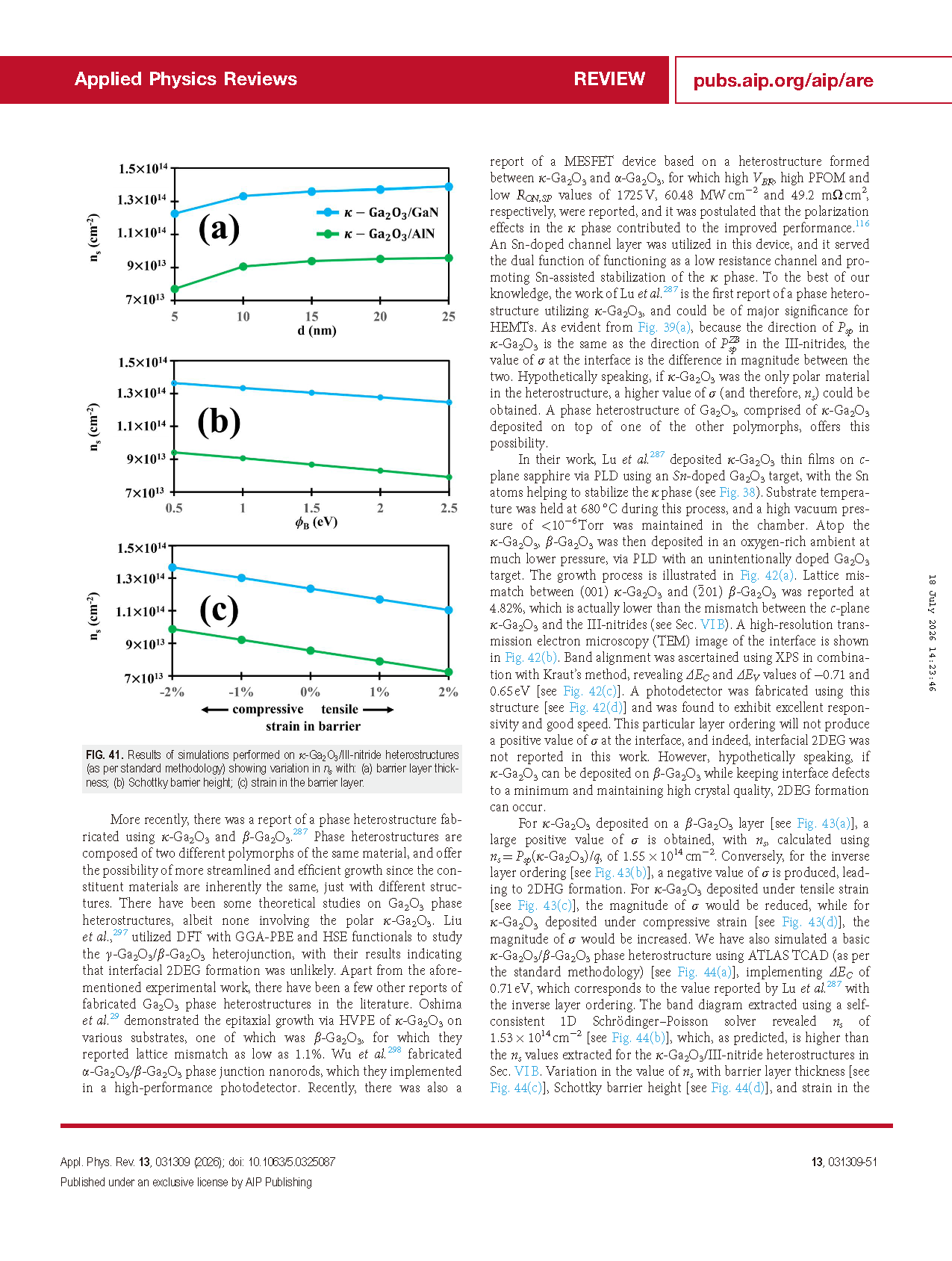
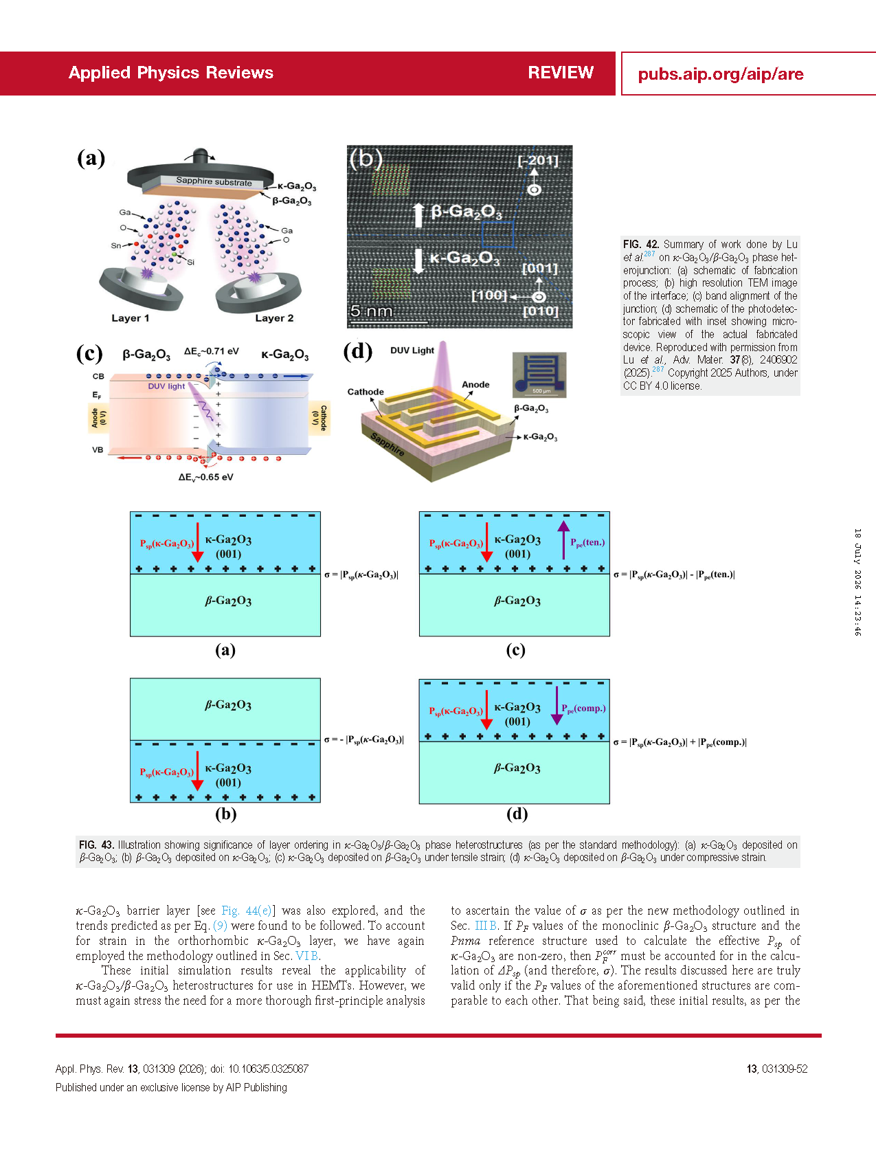
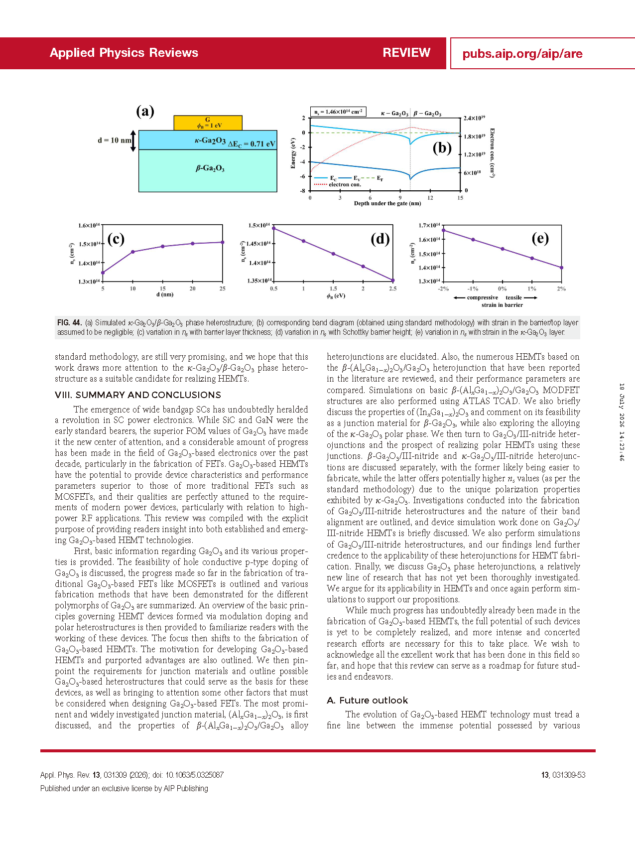
First, basic information regarding Ga₂O₃ and its various properties is provided. The feasibility of hole conductive p-type doping of Ga₂O₃ is discussed, the progress made so far in the fabrication of traditional Ga₂O₃-based FETs like MOSFETs is outlined and various fabrication methods that have been demonstrated for the different polymorphs of Ga₂O₃ are summarized. An overview of the basic principles governing HEMT devices formed via modulation doping and polar heterostructures is then provided to familiarize readers with the working of these devices. The focus then shifts to the fabrication of Ga₂O₃-based HEMTs. The motivation for developing Ga₂O₃-based HEMTs and purported advantages are also outlined. We then pinpoint the requirements for junction materials and outline possible Ga₂O₃-based heterostructures that could serve as the basis for these devices, as well as bringing to attention some other factors that must be considered when designing Ga₂O₃-based FETs. The most prominent and widely investigated junction material, (AlₓGa₁₋ₓ)₂O₃, is first discussed, and the properties of β-(AlₓGa₁₋ₓ)₂O₃/Ga₂O₃ alloy heterojunctions are elucidated. Also, the numerous HEMTs based on the β-(AlₓGa₁₋ₓ)₂O₃/Ga₂O₃ heterojunction that have been reported in the literature are reviewed, and their performance parameters are compared. Simulations on basic β-(AlₓGa₁₋ₓ)₂O₃/Ga₂O₃ MODFET structures are also performed using ATLAS TCAD. We also briefly discuss the properties of (InₓGa₁₋ₓ)₂O₃ and comment on its feasibility as a junction material for β-Ga₂O₃, while also exploring the alloying of the κ-Ga₂O₃ polar phase. We then turn to Ga₂O₃/III-nitride heterojunctions and the prospect of realizing polar HEMTs using these junctions. β-Ga₂O₃/III-nitride and κ-Ga₂O₃/III-nitride heterojunctions are discussed separately, with the former likely being easier to fabricate, while the latter offers potentially higher nₛ values (as per the standard methodology) due to the unique polarization properties exhibited by κ-Ga₂O₃. Investigations conducted into the fabrication of Ga₂O₃/III-nitride heterostructures and the nature of their band alignment are outlined, and device simulation work done on Ga₂O₃/III-nitride HEMTs is briefly discussed. We also perform simulations of Ga₂O₃/III-nitride heterostructures, and our findings lend further credence to the applicability of these heterojunctions for HEMT fabrication. Finally, we discuss Ga₂O₃ phase heterojunctions, a relatively new line of research that has not yet been thoroughly investigated. We argue for its applicability in HEMTs and once again perform simulations to support our propositions.
While much progress has undoubtedly already been made in the fabrication of Ga₂O₃-based HEMTs, the full potential of such devices is yet to be completely realized, and more intense and concerted research efforts are necessary for this to take place. We wish to acknowledge all the excellent work that has been done in this field so far, and hope that this review can serve as a roadmap for future studies and endeavors.
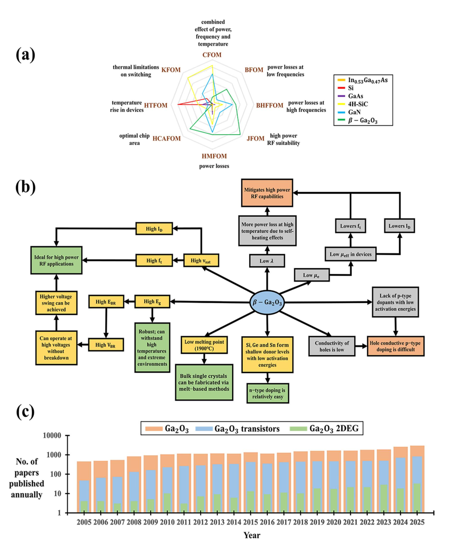
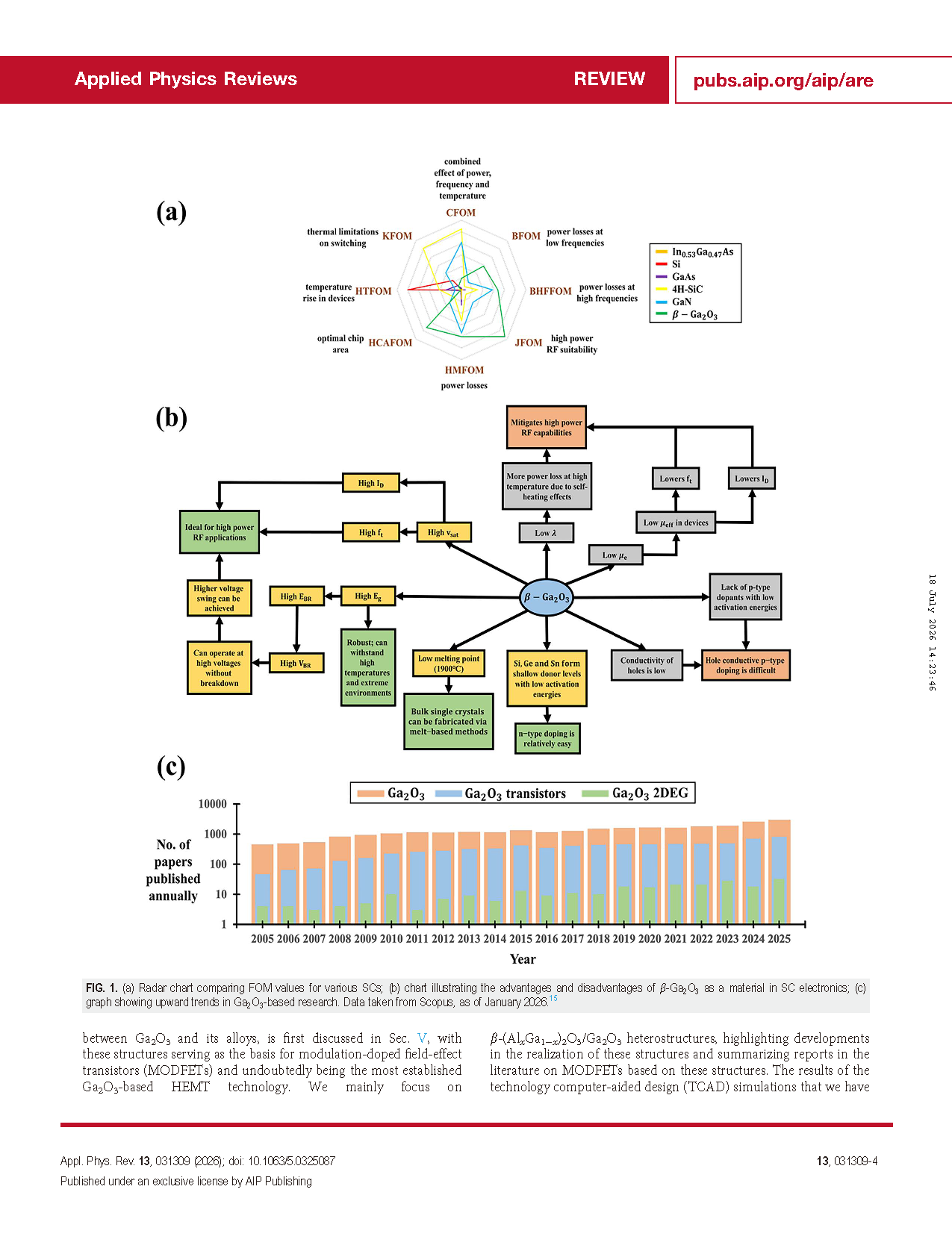
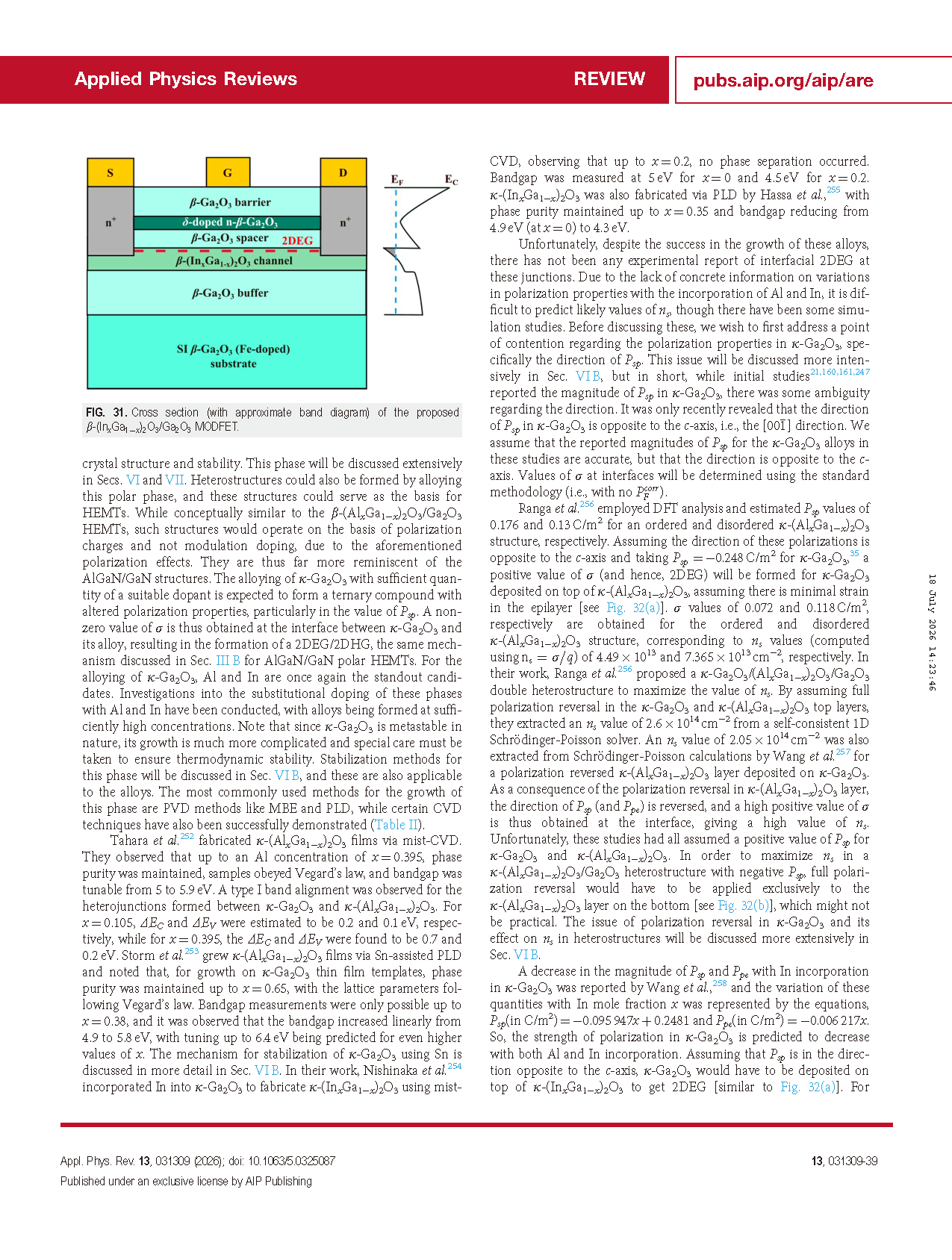
FIG. 1. (a) Radar chart comparing FOM values for various SCs; (b) chart illustrating the advantages and disadvantages of β-Ga₂O₃ as a material in SC electronics; (c) graph showing upward trends in Ga₂O₃-based research. Data taken from Scopus, as of January 2026.
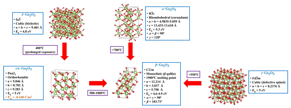
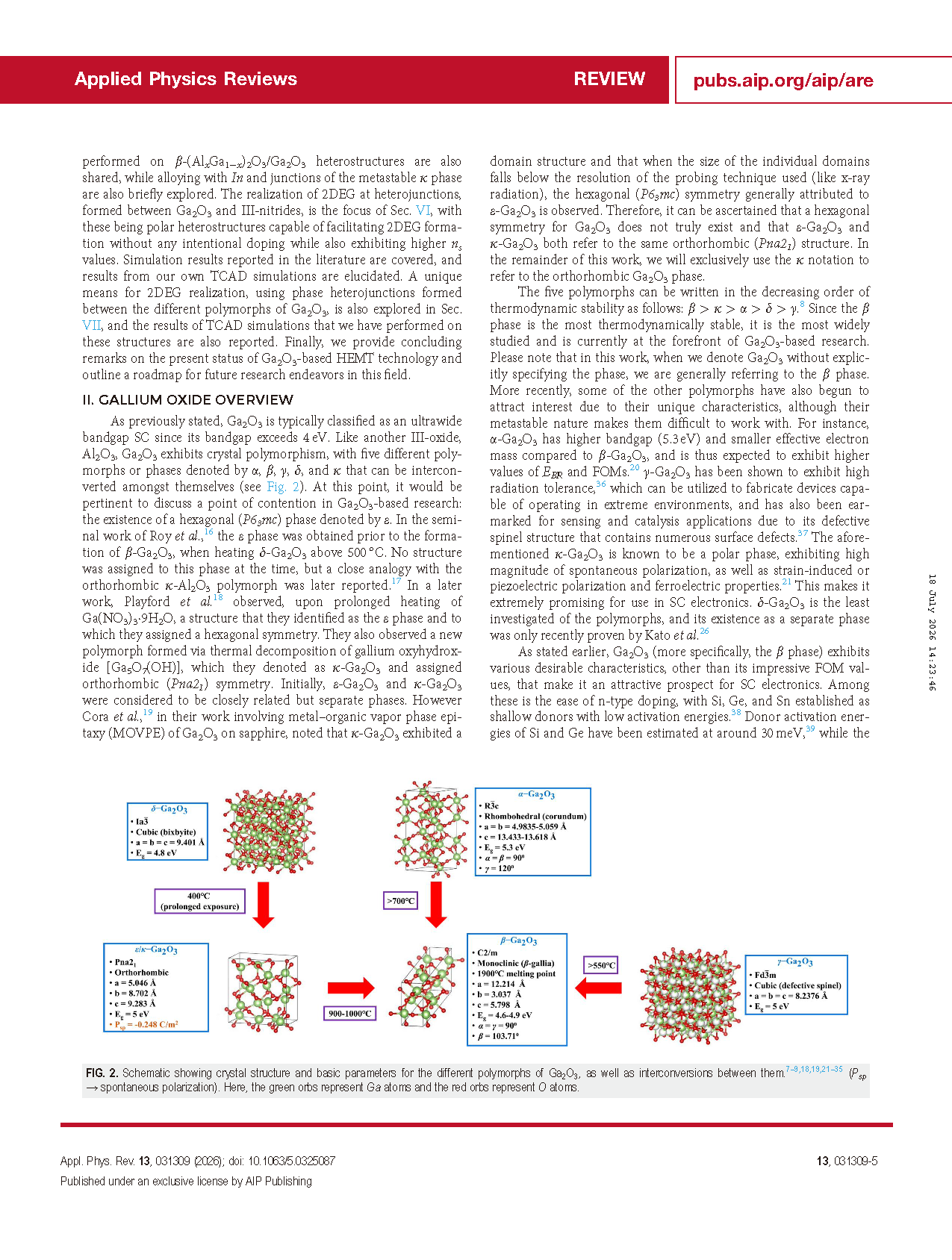
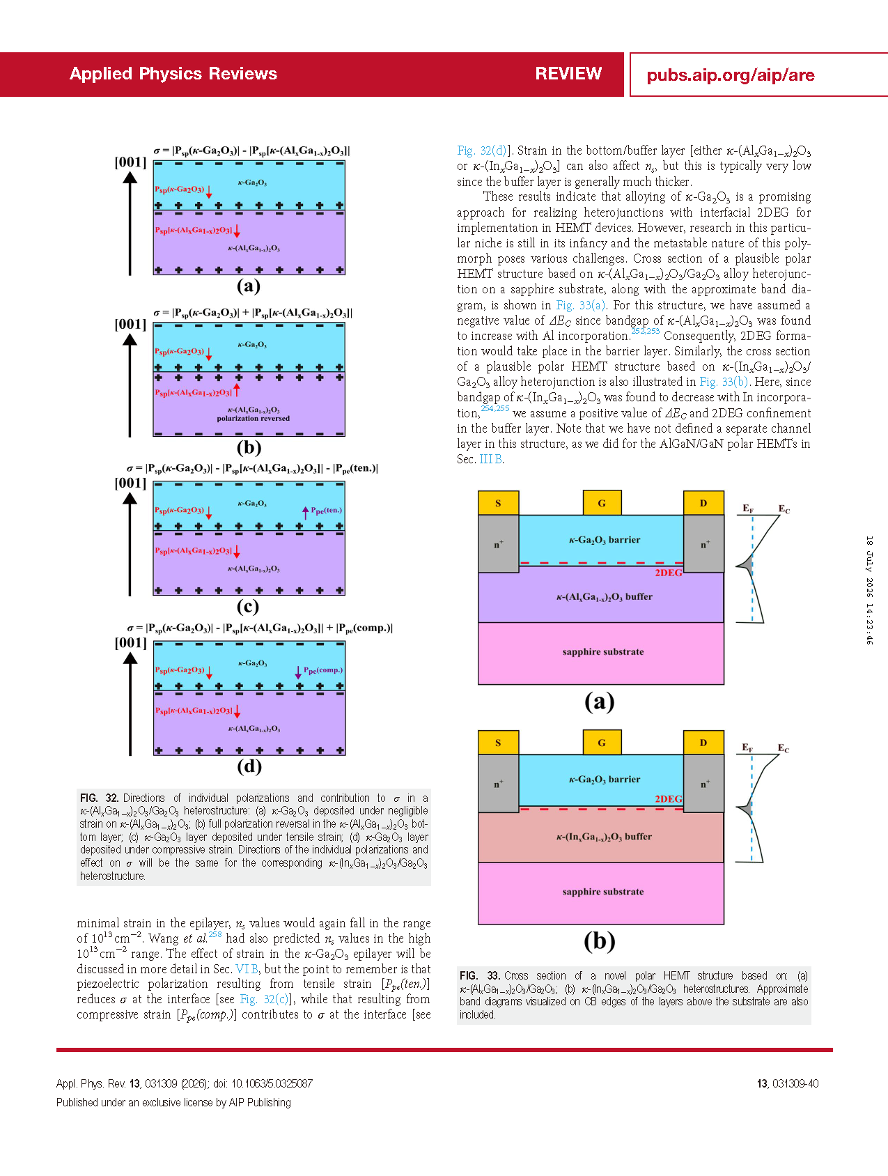
FIG. 2. Schematic showing crystal structure and basic parameters for the different polymorphs of Ga₂O₃, as well as interconversions between them. (Pₛₚ → spontaneous polarization). Here, the green orbs represent Ga atoms and the red orbs represent O atoms.
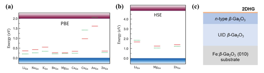
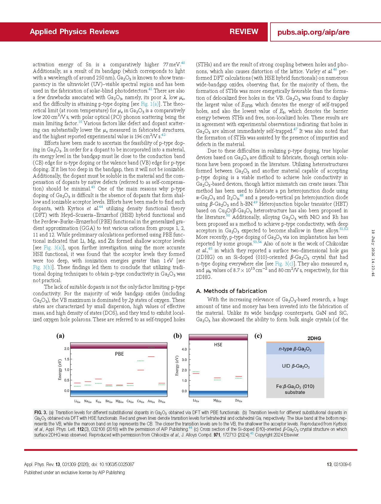
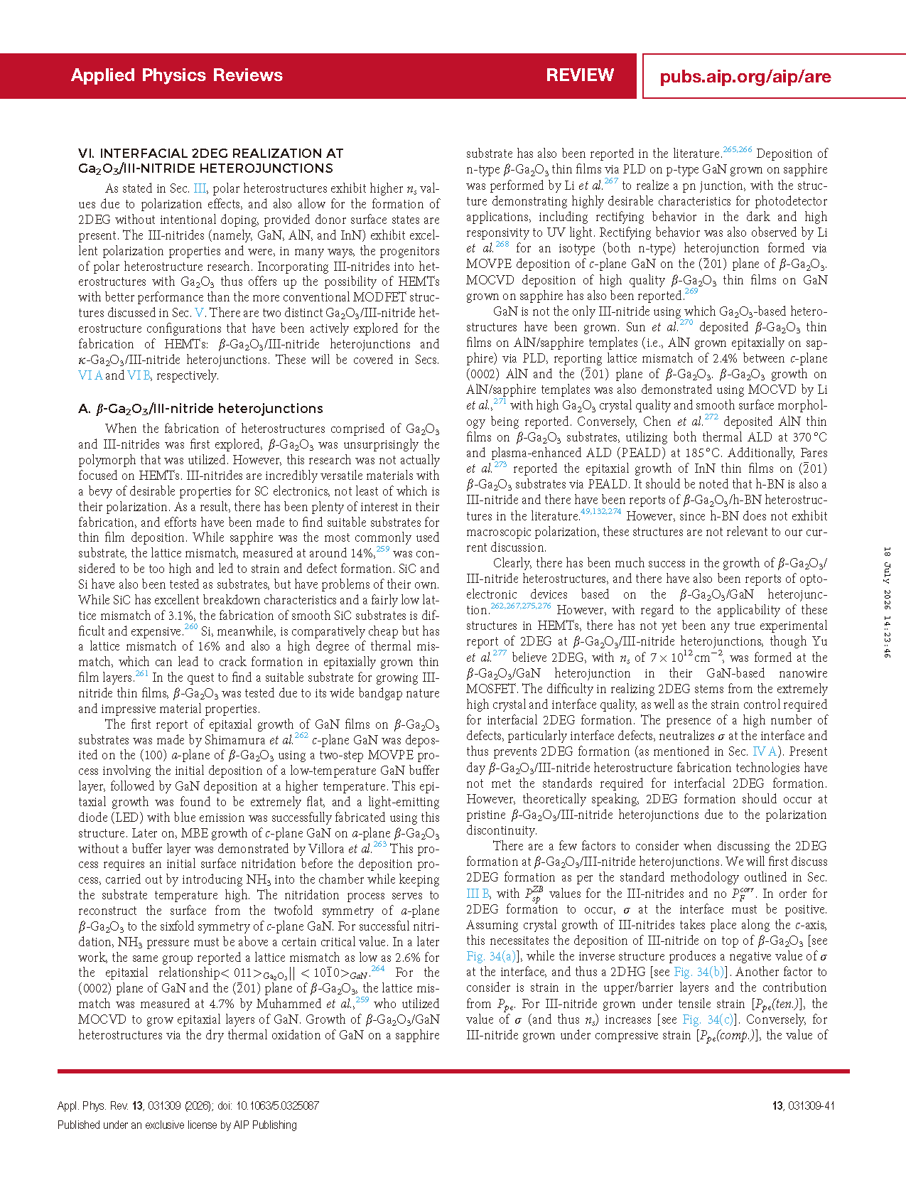
FIG. 3. (a) Transition levels for different substitutional dopants in Ga₂O₃ obtained via DFT with PBE functionals. (b) Transition levels for different substitutional dopants in Ga₂O₃ obtained via DFT with HSE functionals. Red and green lines denote transition levels for tetrahedral and octahedral Ga, respectively. The blue band at the bottom represents the VB, while the maroon band on top represents the CB. The closer the transition levels are to the VB, the shallower the acceptor levels. (c) Cross section of the Si-doped (010)-oriented β-Ga₂O₃ crystal structure on which surface 2DHG was observed.
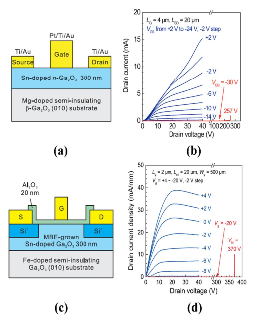
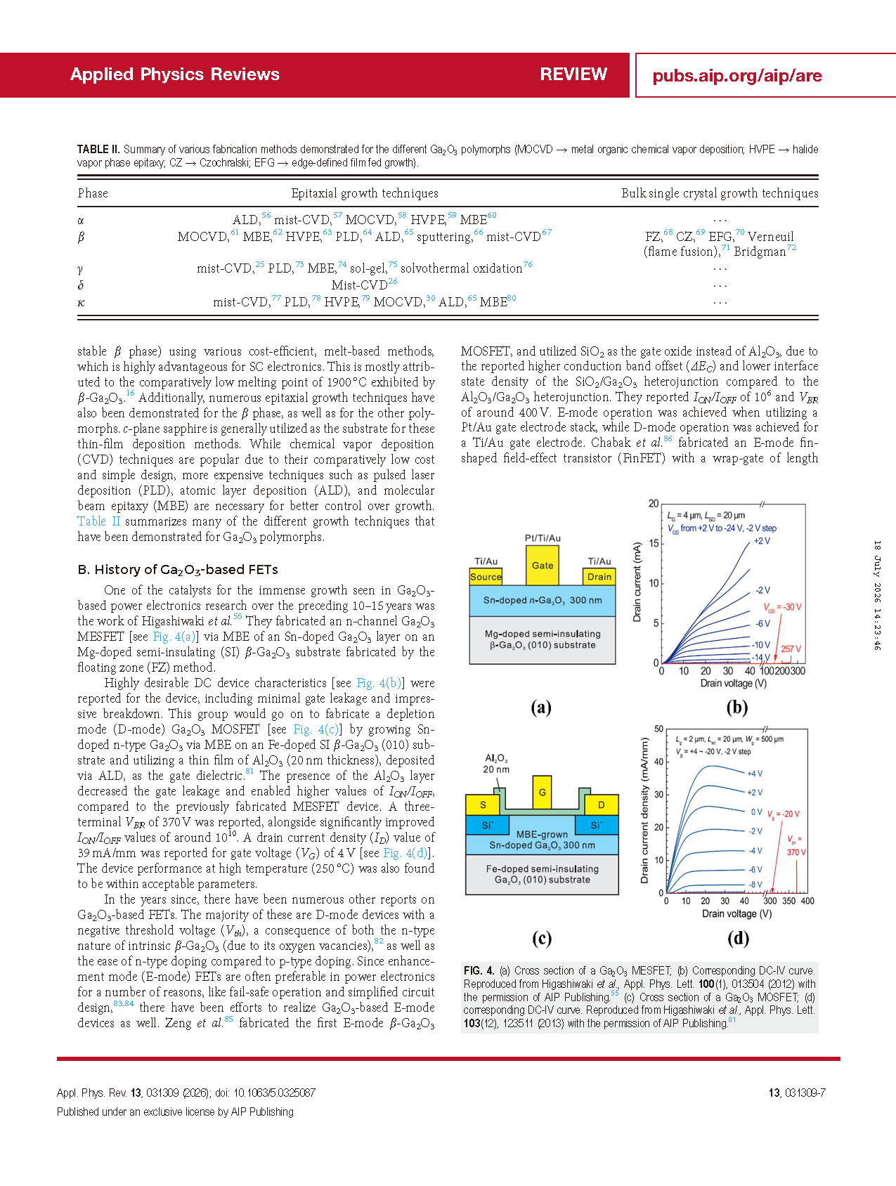
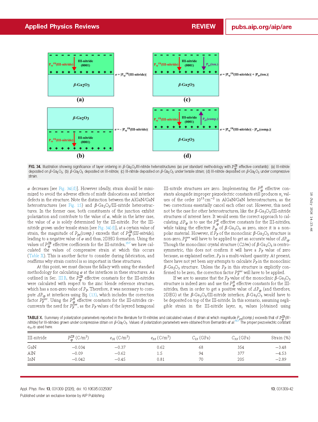
FIG. 4. (a) Cross section of a Ga₂O₃ MESFET; (b) Corresponding DC-IV curve. (c) Cross section of a Ga₂O₃ MOSFET; (d) corresponding DC-IV curve.
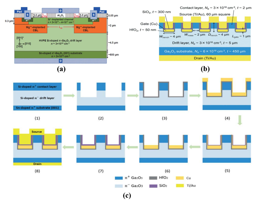
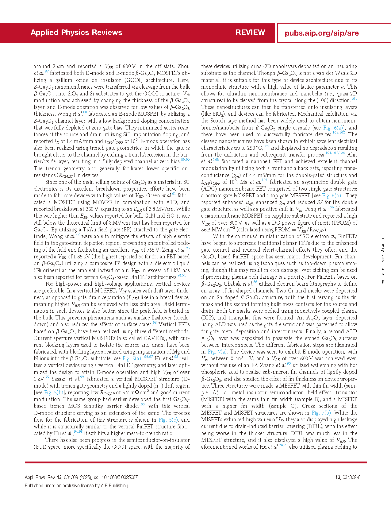
FIG. 5. (a) Cross section of a Ga₂O₃ CAVET with Mg-doped current blocking layer. (b) Cross section of a Ga₂O₃ vertical trench gate MOSFET. (c) Process flow for the fabrication of a Ga₂O₃ vertical trench gate MOSFET: (1) growth of epitaxial layers on β-Ga₂O₃ substrate using HVPE, (2) trench formation via photolithography and plasma etching, (3) deposition of HfO₂ gate dielectric by ALD, (4) deposition of Cu gate metal by electron-beam evaporation, (5) deposition of SiO₂ film and removal of excess material on top of each mesa by chemical mechanical polishing, (6) removal of Cu and SiO₂ from trench sidewalls by wet etching, (7) formation of SiO₂ isolation layer by RF sputtering and CMP, (8) deposition of source/drain electrode metals.
DOI:
doi.org/10.1063/5.0325087
Instruction
Official Account

Cooperation
Top
