


Researchers from Hubei University have published a dissertation titled "Doping-Engineered Modulation of Oxygen Vacancy Formation Energy in Gallium Oxide for High-Performance Solar-Blind UV Photodetectors" in Rare Metals.
Background
Solar-blind ultraviolet photodetectors eliminate visible light interference and play irreplaceable roles in power grid corona detection, fire alarm, UV communication and underwater imaging. β-Ga₂O₃ with intrinsic 4.6–4.9 eV solar-blind bandgap is the ideal candidate material. Intrinsic β-Ga₂O₃ generates massive oxygen vacancy defects during growth. Oxygen vacancies act as shallow donors to raise dark current, and deep traps to capture photocarriers, leading to slow response and blurry imaging. Existing N, Zn, Zr doping methods only slightly reduce defects and fail to simultaneously achieve ultrahigh PDCR, fast response and high detectivity. PLD/ALD equipment costs are high, while sol-gel introduces organic impurities. Low-cost CVD-compatible doping routes are scarce. Previous Mg-doped Ga₂O₃ works only characterize electrical performance without DFT quantitative analysis of vacancy formation energy. No integrated research combining defect suppression, bandgap widening and imaging demonstration has been reported, forming a major gap for industrial low-cost solar-blind photodetectors.
Abstract
Solar-blind ultraviolet (UV) photodetectors (SBPDs) play a critical role in applications including UV communication and fire warning systems. Gallium oxide (Ga₂O₃) has emerged as a promising material due to its wide bandgap and low cost, but suffers from high dark current and slow response speed caused by oxygen vacancy (VO) defects. This work proposes a defect engineering strategy using Mg doping to modulate oxygen vacancy formation energy, fabricating Mg-doped β-Ga₂O₃ (β-Ga₂O₃:Mg) thin-film photodetectors via low-cost chemical vapor deposition (CVD). The doping of Mg suppresses the generation of VO and broadens the bandgap, which significantly improves the photodetection performance. Experimental results demonstrate that Mg doping achieves a 23% reduction in VO concentration and increases the bandgap from 4.72 to 4.87 eV. The optimized device exhibits a photo to dark current ratio of 10⁶ (compared to 10⁴ for pristine Ga₂O₃), ultralow dark current of 2.67 ×10⁻¹² A at 20 V, detectivity of 1.576 ×10¹⁴ Jones and response times reduced to 14.7 ms (rise)/7 ms (decay) (318.1 ms/187.5 ms for undoped devices). The photodetector successfully demonstrates UV single-point scanning imaging, clearly displaying “H,” “U,” and “I” letter patterns, and maintains stable performance during 1500-second continuous illumination. This work combines defect engineering with low-cost fabrication to provide a cost-effective reliable solution for high-performance SBPDs.
Highlights
Propose Mg doping defect engineering route based on low-cost CVD to raise oxygen vacancy formation energy and suppress VOconcentration by 23%.
Realize bandgap widening from 4.72 eV to 4.87 eV, obtain PDCR up to 10⁶and ultralow dark current of 2.67 ×10⁻¹² A @ 20 V.
Shorten rise/decay response time to 14.7 ms / 7 ms, greatly eliminate carrier trapping induced by oxygen vacancy deep defects.
Complete DFT theoretical verification and single-point UV imaging test, prove practical application potential of Mg-doped Ga₂O₃ SBPD.
Conclusion
This study employs a simplified CVD approach to fabricate Mg-doped β-Ga₂O₃ thin films and metal-semiconductor-metal ultraviolet photodetectors. The doping of Mg element was found to have a significant inhibitory effect on the oxygen vacancies present in gallium oxide, either directly or indirectly, by experimental methods such as XPS, EPR and Raman. DFT simulations further validate the underlying mechanism: Mg incorporation elevates VO formation energy, thereby inhibiting VO defect generation. The fabricated β-Ga₂O₃:Mg photodetectors exhibit exceptional performance metrics: ultralow dark current of 2.67 ×10⁻¹² A at 20 V, high PDCR of approximately 10⁶, rapid response times of 14.7 ms (rise)/7 ms (decay), and D* of 1.576 ×10¹⁴ Jones. Remarkably, these devices maintain stable performance during 1500 s continuous illumination without significant degradation. The successful demonstration of single-point imaging with clear letter pattern recognition (“H,” “U,” “T”) highlights the commercial potential of this technology. In summary, this work advances Ga₂O₃ doping methodologies, achieves an optimal balance between D* and response time, and provides a new technical pathway for optimizing solar-blind UV photodetector performance.
Project Support
This work was financially supported by the Major Program of Hubei Province (Grant No. 2023BAA009) and the Natural Science Foundation of Hubei Province (Grant No. 2023AFB623).
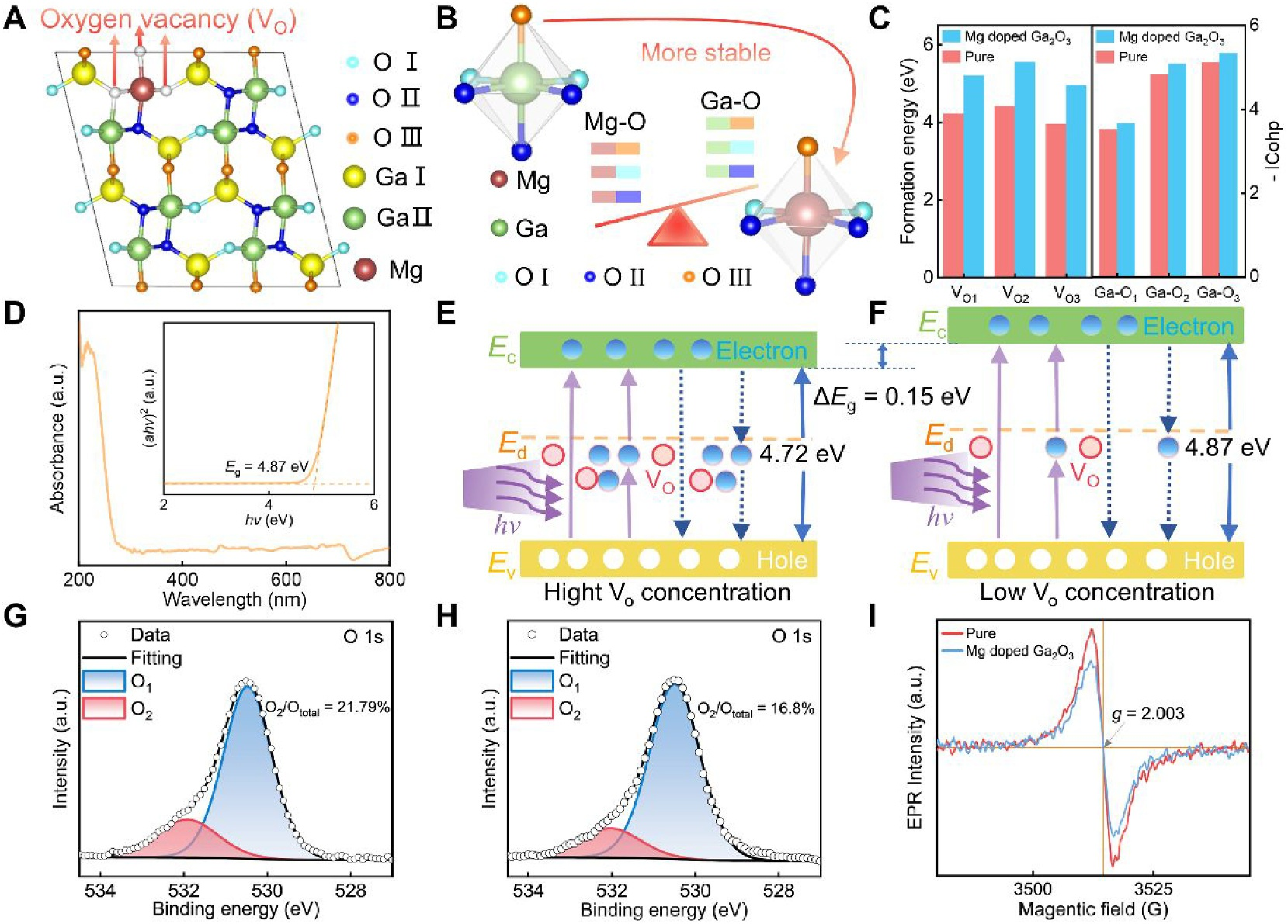
FIGURE 1 | Mechanism of Mg element doping inhibiting oxygen vacancy defects in β-Ga₂O₃. (A) The unit cell structure diagram of Mg-doped gallium oxide with oxygen vacancies. (B) Influence of bond strength and structure before and after Mg doping. (C) Left half shows the formation energy of oxygen vacancies in β-Ga₂O₃ before and after Mg doping. Right half shows the minus integrated COHPs (‐ICOHP) of the three different Ga‐O bonds and the three different Mg‐O bonds. (D) The optical absorbance of Mg-doped β-Ga₂O₃ films (the inset is the band gap of β-Ga₂O₃:Mg films). (E, F) Diagram of the effect of different VO concentrations and band structure changes on optoelectronic properties of devices. (G) O 1s spectra of β-Ga₂O₃. (H) O 1s spectra of β-Ga₂O₃:Mg. (I) EPR analysis plots before and after Mg doping.
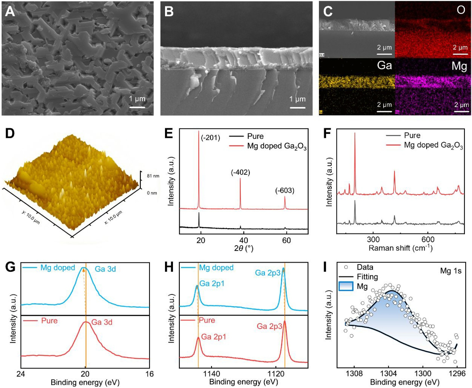
FIGURE 2 | Structural characterization of β-Ga₂O₃ and β-Ga₂O₃:Mg. (A, B) Planar and cross-sectional SEM images of β-Ga₂O₃:Mg thin film. (C) Cross-sectional EDS mapping of β-Ga₂O₃:Mg thin film. (D) 3D AFM of β-Ga₂O₃:Mg thin film. (E) XRD pattern of β-Ga₂O₃ and β-Ga₂O₃:Mg. (F) Raman spectra of β-Ga₂O₃ and β-Ga₂O₃:Mg. (G–I) XPS elemental peak analysis. (G) The XPS peak fitting of Ga 3d. (H) The XPS peak fitting of Ga 2p. (I) Peak fitting plots of elemental Mg.
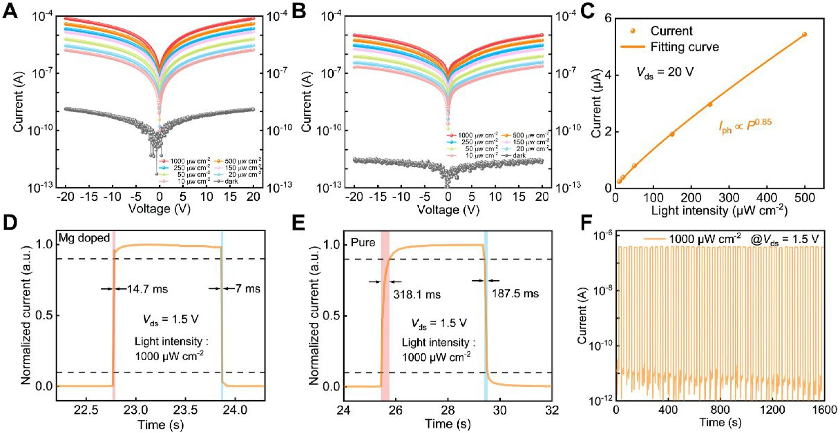
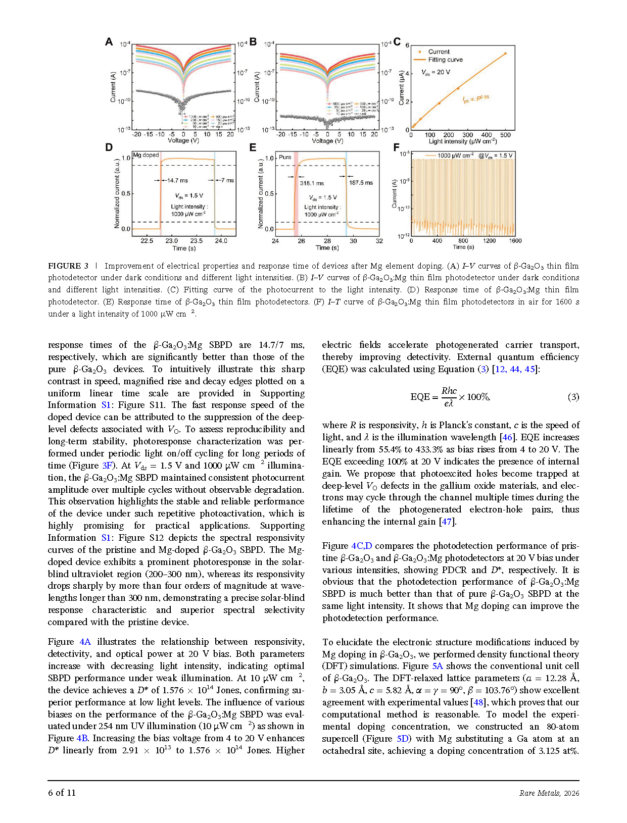
FIGURE 3 | Improvement of electrical properties and response time of devices after Mg element doping. (A) I–V curves of β-Ga₂O₃ thin film photodetector under dark conditions and different light intensities. (B) I-V curves of β-Ga₂O₃:Mg thin film photodetector under dark conditions and different light intensities. (C) Fitting curve of the photocurrent to the light intensity. (D) Response time of β-Ga₂O₃:Mg thin film photodetector. (E) Response time of β-Ga₂O₃ thin film photodetectors. (F) I-T curve of β-Ga₂O₃:Mg thin film photodetectors in air for 1600 s under a light intensity of 1000 μW cm⁻².
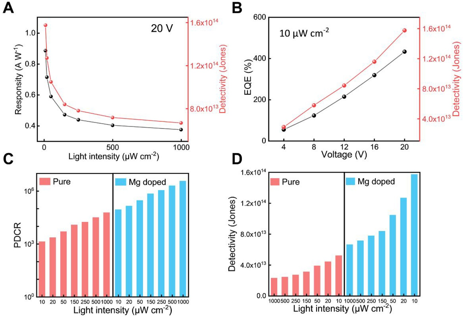
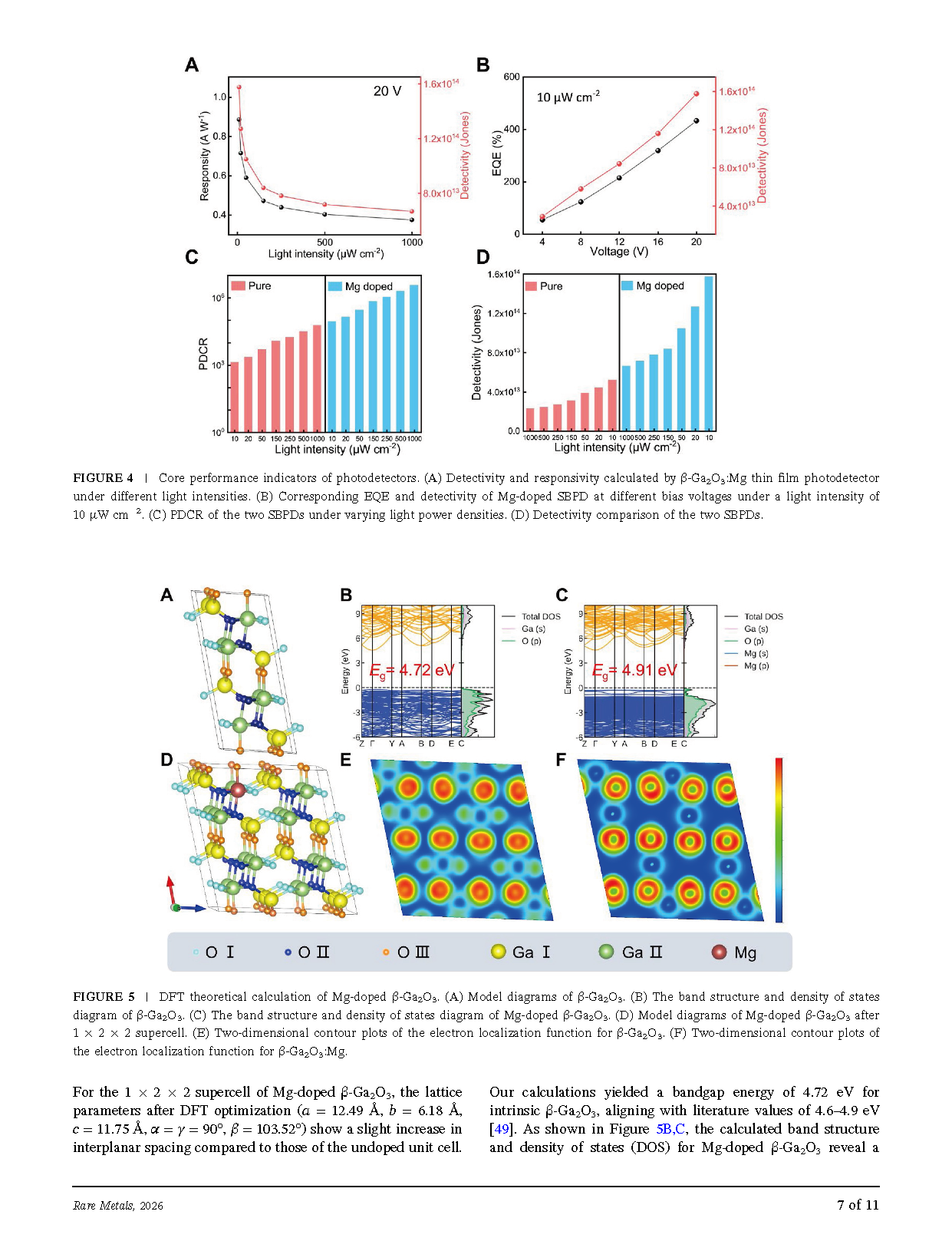
FIGURE 4 | Core performance indicators of photodetectors. (A) Detectivity and responsivity calculated by β-Ga₂O₃:Mg thin film photodetector under different light intensities. (B) Corresponding EQE and detectivity of Mg-doped SBPD at different bias voltages under a light intensity of 10 μW cm⁻². (C) PDCR of the two SBPDs under varying light power densities. (D) Detectivity comparison of the two SBPDs.
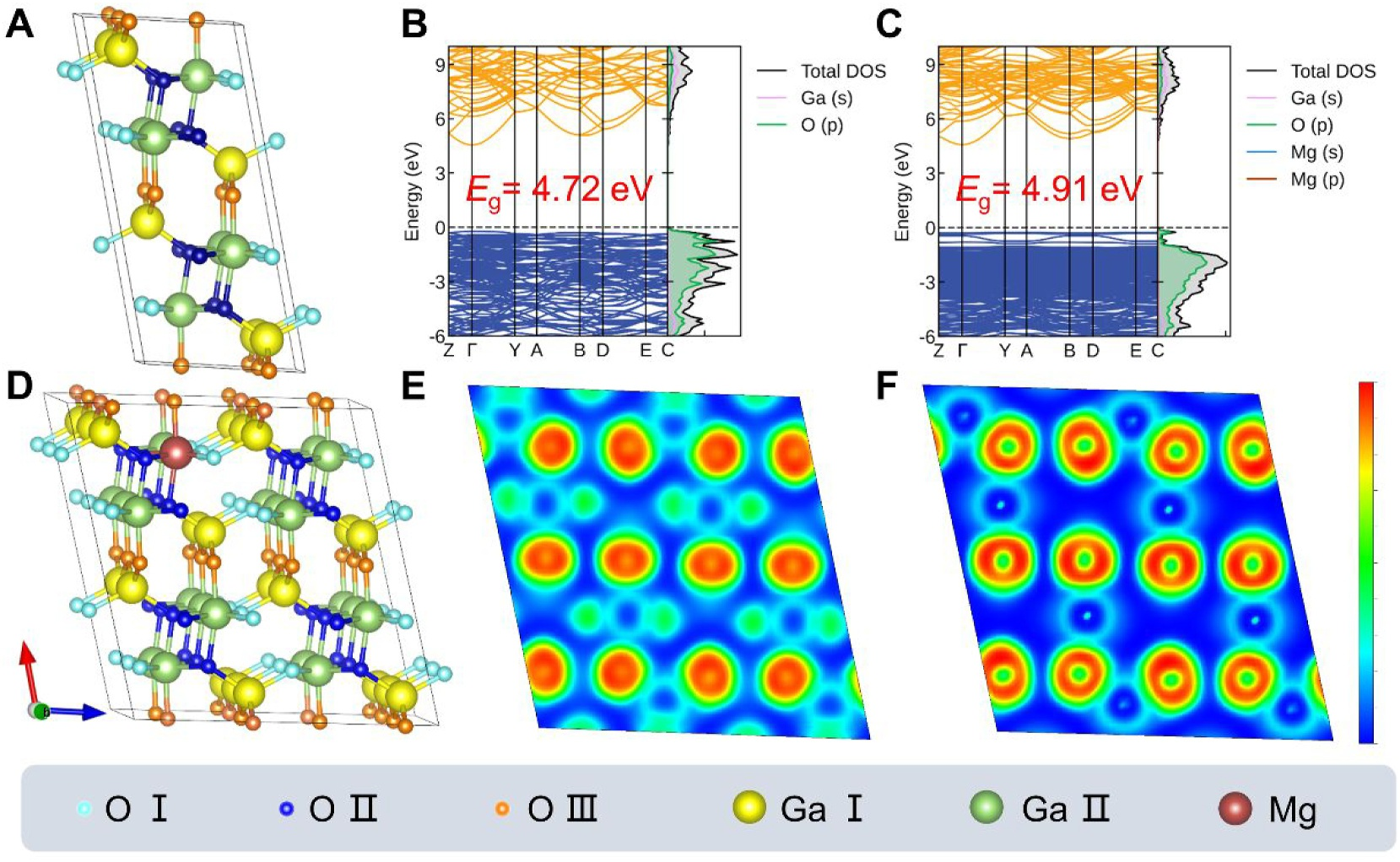
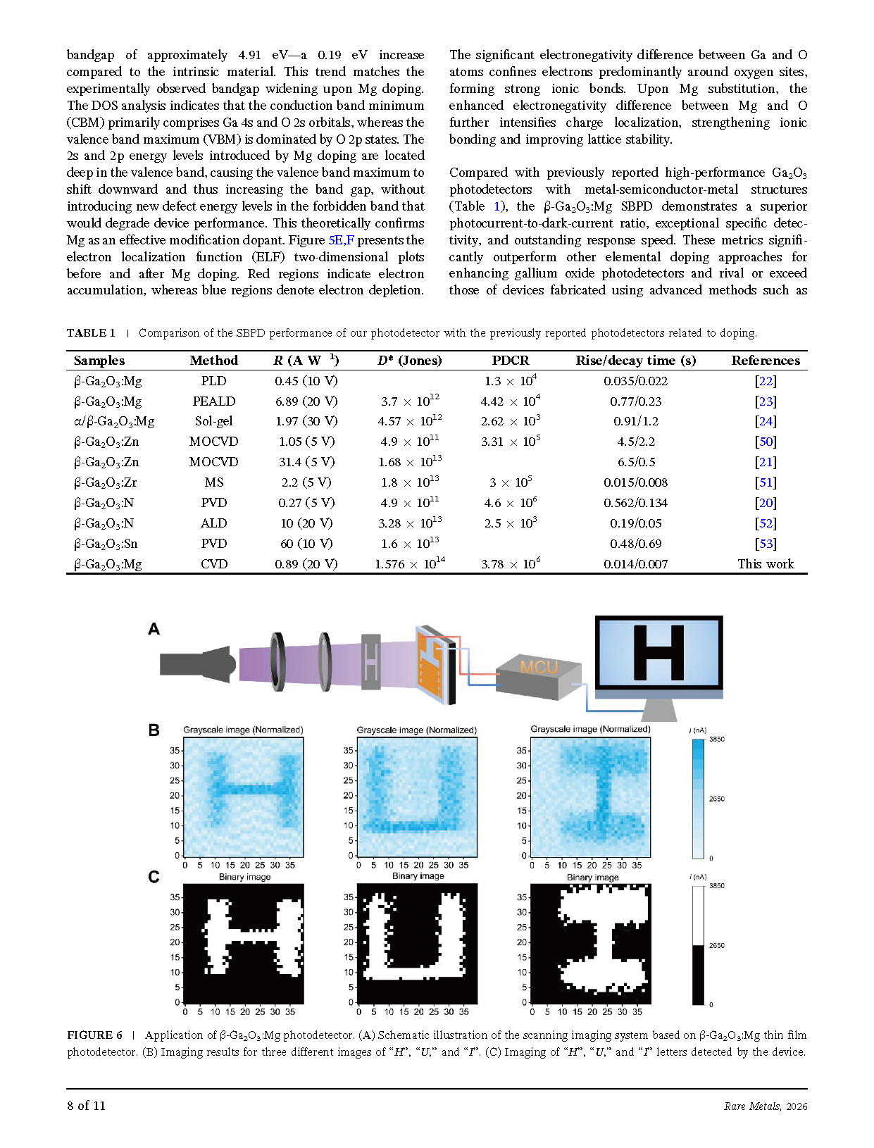
FIGURE 5 | DFT theoretical calculation of Mg-doped β-Ga₂O₃. (A) Model diagrams of β-Ga₂O₃. (B) The band structure and density of states diagram of β-Ga₂O₃. (C) The band structure and density of states diagram of Mg-doped β-Ga₂O₃. (D) Model diagrams of Mg-doped β-Ga₂O₃ after 1 × 2 × 2 supercell. (E) Two-dimensional contour plots of the electron localization function for β-Ga₂O₃. (F) Two-dimensional contour plots of the electron localization function for β-Ga₂O₃:Mg.
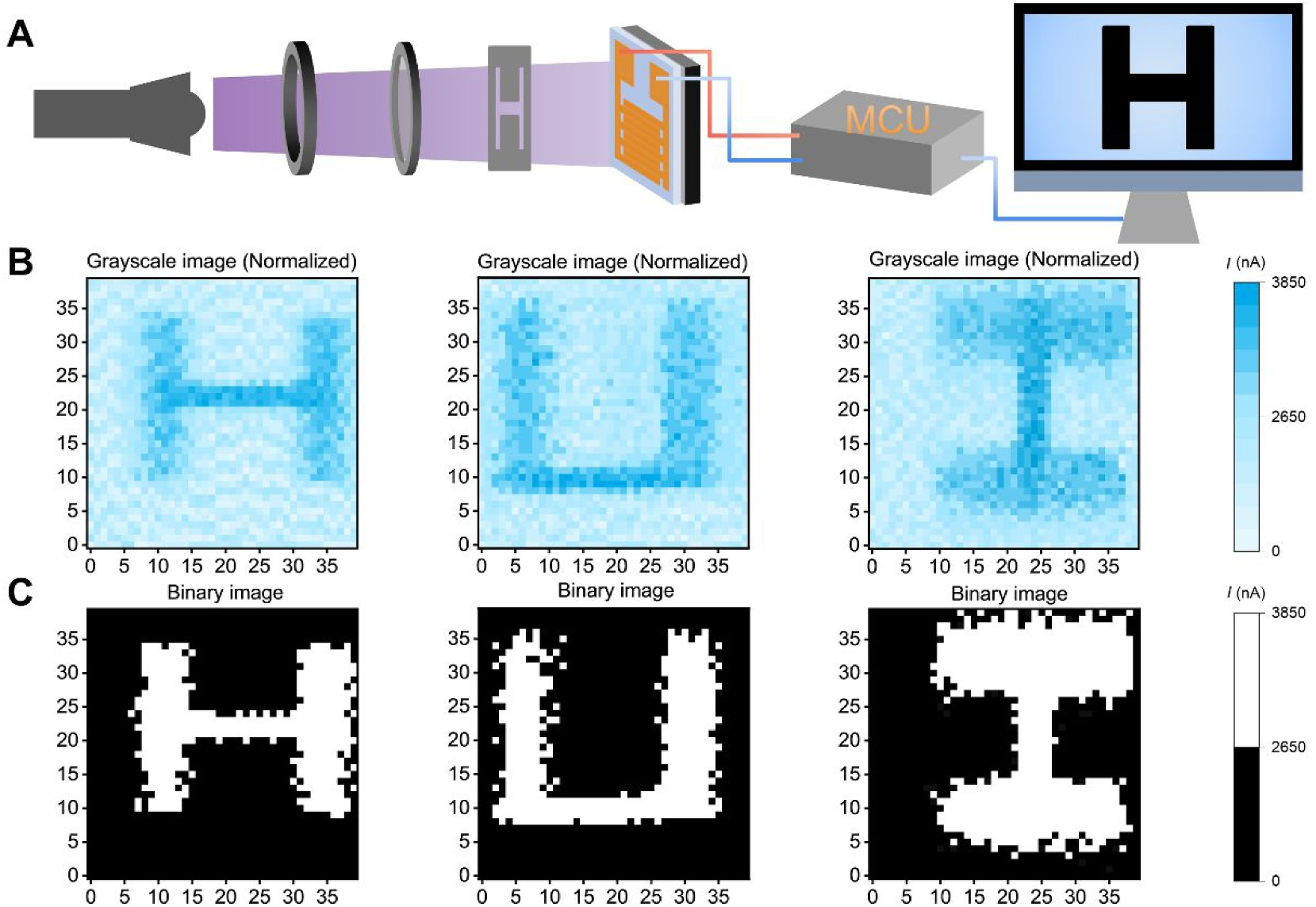
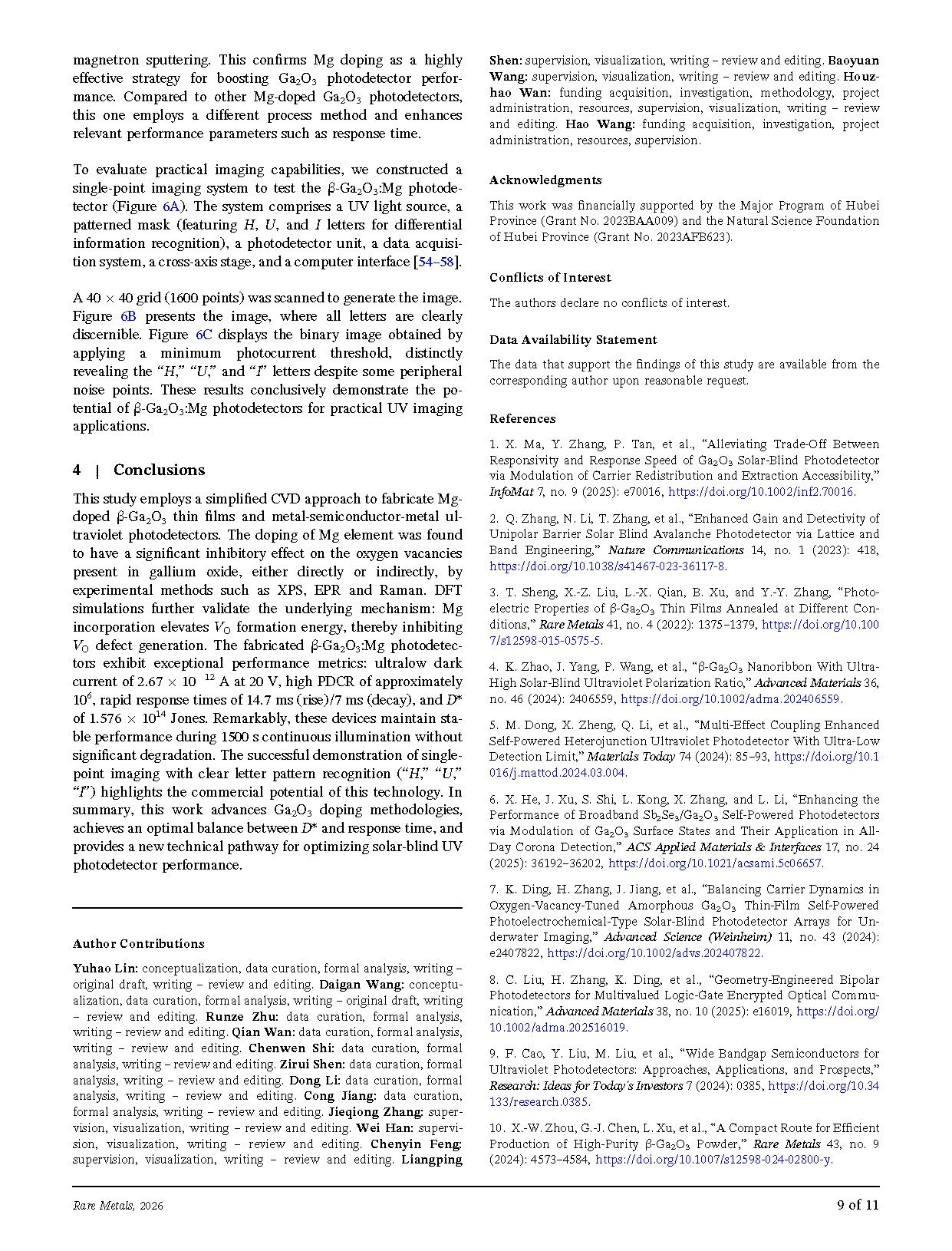
FIGURE 6 | Application of β‐Ga₂O₃:Mg photodetector. (A) Schematic illustration of the scanning imaging system based on β‐Ga₂O₃:Mg thin film photodetector. (B) Imaging results for three different images of “H”, “U,” and “I”. (C) Imaging of “H”, “U,” and “I” letters detected by the device.
DOI:
doi.org/10.1002/rar2.70478


Instruction
Official Account

Cooperation
Top
