



Researchers from Xiamen University have published a dissertation titled "Interfacial rare-earth oxide-enabled X-ray-tolerant Ga₂O₃ MIS Schottky barrier diodes with significant reverse leakage current suppression" in Materials Today Physics.
Background
Spacecraft and nuclear power systems demand power semiconductors with both high breakdown voltage and ionizing radiation resistance. β-Ga₂O₃ with an ultra-wide bandgap of 4.8 eV is ideal for harsh-environment electronics. Conventional Ni/β-Ga₂O₃ Schottky diodes lack dielectric interlayers; X-ray irradiation generates massive interface defects, raising leakage current and degrading blocking capability. Rare-earth Gd₂O₃ features high dielectric constant and strong X-ray attenuation, yet its dual function of boosting breakdown and radiation tolerance remains underexplored. No systematic quantitative analysis on interface traps and Poole-Frenkel transport after irradiation has been reported, and no complete MIS diode architecture combining low on-resistance, kV-class breakdown and X-ray immunity exists, forming an obvious research gap for radiation-hard Ga₂O₃ power devices.
Abstract
Power electronic devices operating in radiation-rich environments, such as space and nuclear facilities, require both high breakdown voltage and radiation tolerance. Gallium oxide (Ga₂O₃) offers an ultra-wide bandgap and a high critical electric field, but its electrical stability can be affected by X-ray-induced charge trapping and defect states. Here, we introduced an ultrathin rare-earth Gd₂O₃ interlayer to fabricate X-ray-tolerant Ni / Gd₂O₃ / β-Ga₂O₃ metal-insulator-semiconductor (MIS) Schottky barrier diodes (SBDs). This interfacial engineering strategy increased the breakdown voltage from 290 V for the conventional Ni / β-Ga₂O₃ SBD to 1001 V for the MIS SBD while maintaining a low specific on-resistance of 2.6 mΩ·cm². Remarkably, after X-ray irradiation, the Gd₂O₃-interlayer MIS SBDs exhibited stable forward characteristics and a three-order-of-magnitude suppression of reverse leakage current at -100 V, contrary to the degradation behavior observed in conventional SBDs. Frequency-dependent conductance analysis revealed that the leakage suppression originated from a reduced interface trap density rather than drift-layer carrier compensation. Temperature-dependent current-voltage analysis confirmed Poole-Frenkel emission as the dominant leakage mechanism, with the extracted emission barrier increasing from 0.73 to 1.33 eV after irradiation, indicating more difficult trap-assisted carrier emission, which also contributed to the suppressed reverse leakage current. Furthermore, the high-atomic-number rare-earth Gd₂O₃ interlayer may modify local X-ray energy deposition near the interface, which is consistent with the reduced contribution of interfacial trap states to leakage transport. These findings highlight rare-earth oxide interfacial engineering as a promising route to simultaneously achieve high breakdown capability and X-ray irradiation tolerance in Ga₂O₃ power devices for harsh-environment applications.
Highlights
Propose ultrathin Gd₂O₃rare-earth interlayer engineering to construct radiation-hard Ni/Gd₂O₃/β-Ga₂O₃ MIS Schottky diodes.
Realize breakdown voltage boosted from 290 V to 1001 V with specific on-resistance kept at 2.6 mΩ·cm².
Achieve three orders of magnitude reverse leakage suppression under -100 V after X-ray irradiation with stable forward performance.
Clarify dual mechanism: reduced interface trap density and elevated Poole-Frenkel emission barrier induced by high-Z Gd₂O₃ X-ray energy modulation.
Conclusion
In summary, we reported an interfacial engineering strategy based on an ultrathin rare-earth Gd₂O₃ interlayer in Ni / Gd₂O₃ / β-Ga₂O₃ MIS SBDs to effectively enhance the device blocking capability and improve the device X-ray irradiation tolerance. After irradiation, the MIS SBDs exhibited nearly unchanged forward characteristics, including Von and Ron,sp with slight Vbr degradation. Notably, the reverse leakage current was suppressed, in contrast to conventional Ni / β-Ga₂O₃ SBDs. Frequency-dependent conductance and C-V measurements revealed a reduced DT and only minor changes in the overall drift-layer carrier concentration, indicating that leakage current suppression originates from a modified near-interface trap response rather than drift-layer carrier compensation. J-V-T analysis confirmed that Poole-Frenkel emission dominated the reverse leakage transport through trap states in the highfield depletion region. The increased emission barrier after irradiation suggested that carrier emission from trap states became more difficult, thereby contributing to the suppressed leakage current. In addition, the high-Z rare-earth Gd₂O₃ interlayer may locally modify X-ray energy deposition near the interface, consistent with the reduced contribution of interfacial trap states to leakage transport. These findings demonstrate that rare-earth oxide interfacial engineering is an effective strategy for simultaneously improving breakdown capability and x-ray irradiation tolerance in β-Ga₂O₃ SBDs for harsh-environment power electronics.
Project Support
This work was supported by the National Natural Science Foundation of China under Grant 62171396, the Shenzhen Science and Technology Program under Grant JCYJ20240813145617023.
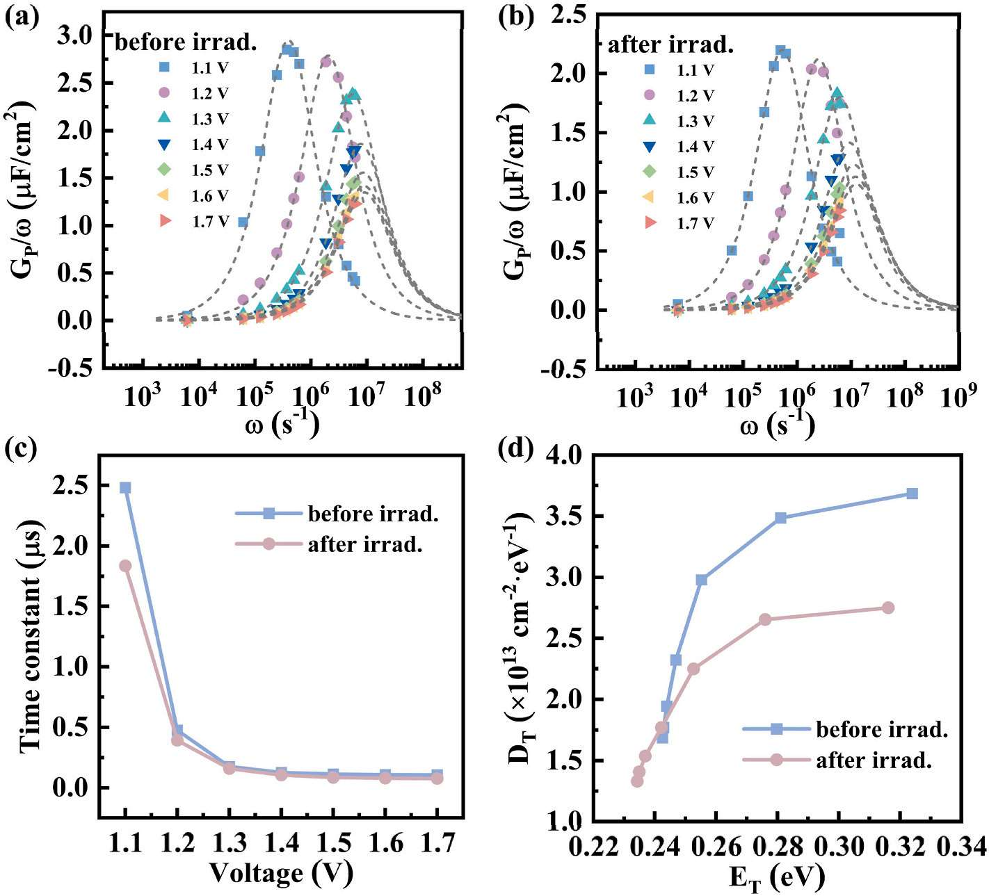
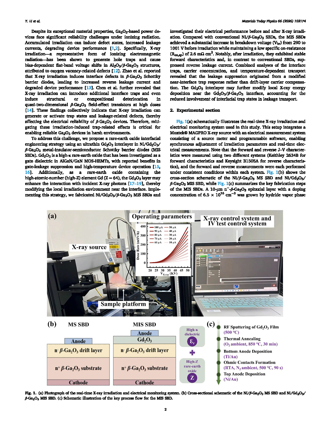
Fig. 1. (a) Photograph of the real-time X-ray irradiation and electrical monitoring system. (b) Cross-sectional schematic of the Ni / β-Ga₂O₃ MS SBD and Ni / Gd₂O₃ / β-Ga₂O₃ MIS SBD. (c) Schematic illustration of the key process flow for the MIS SBD.
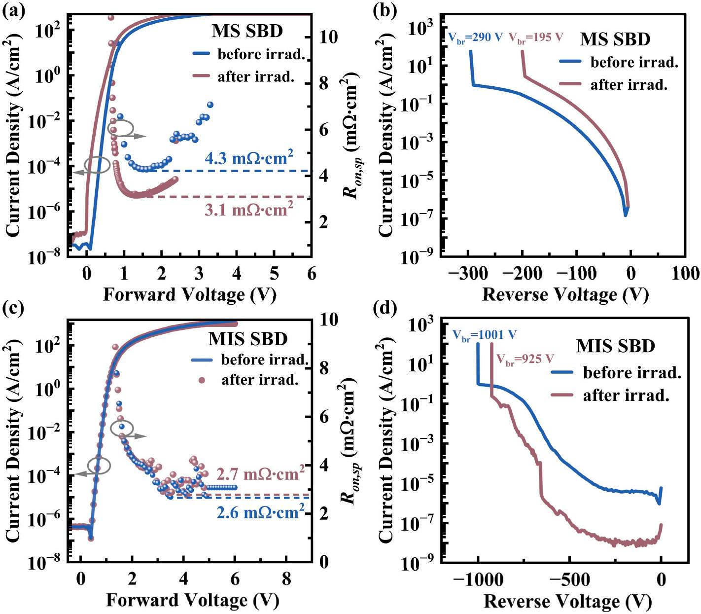
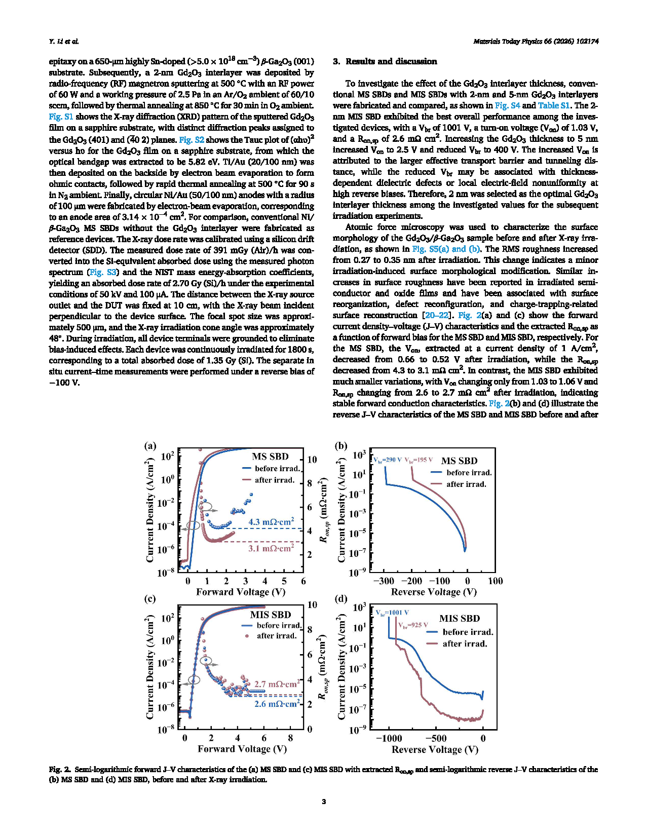
Fig. 2. Semi-logarithmic forward J-V characteristics of the (a) MS SBD and (c) MIS SBD with extracted Ron,sp and semi-logarithmic reverse J-V characteristics of the (b) MS SBD and (d) MIS SBD, before and after X-ray irradiation.
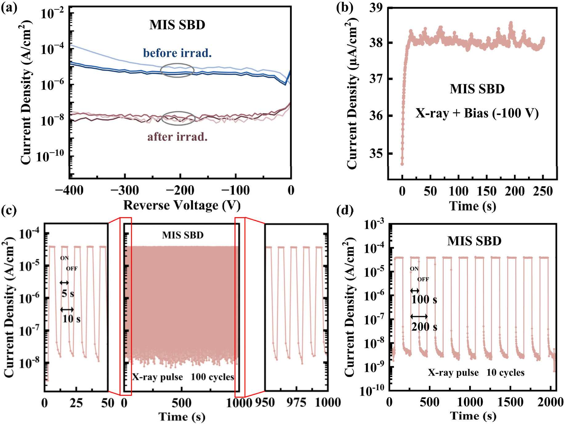
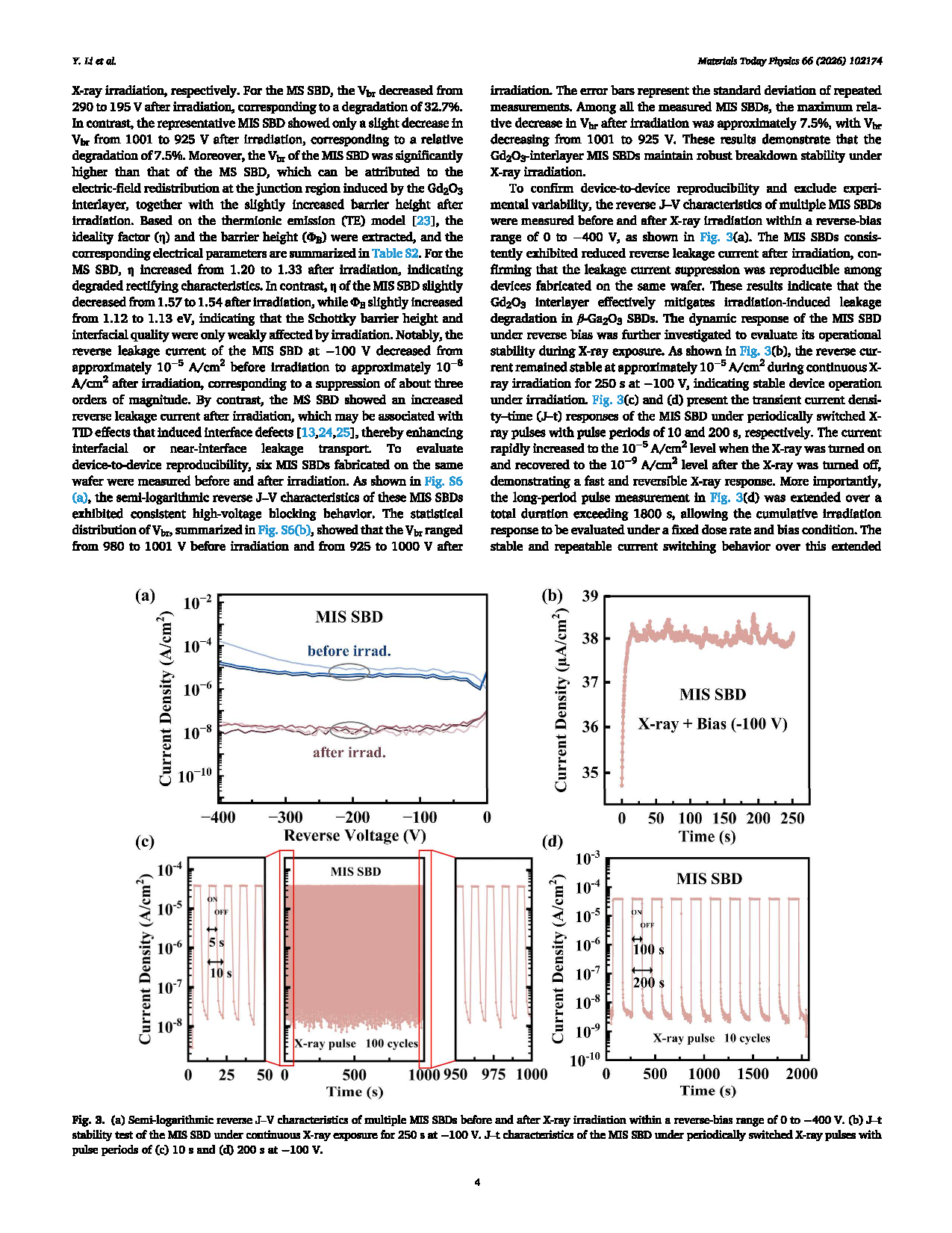
Fig. 3. (a) Semi-logarithmic reverse J-V characteristics of multiple MIS SBDs before and after X-ray irradiation within a reverse-bias range of 0 to -400 V. (b) J-t stability test of the MIS SBD under continuous X-ray exposure for 250 s at -100 V. J-t characteristics of the MIS SBD under periodically switched X-ray pulses with pulse periods of (c) 10 s and (d) 200 s at -100 V.
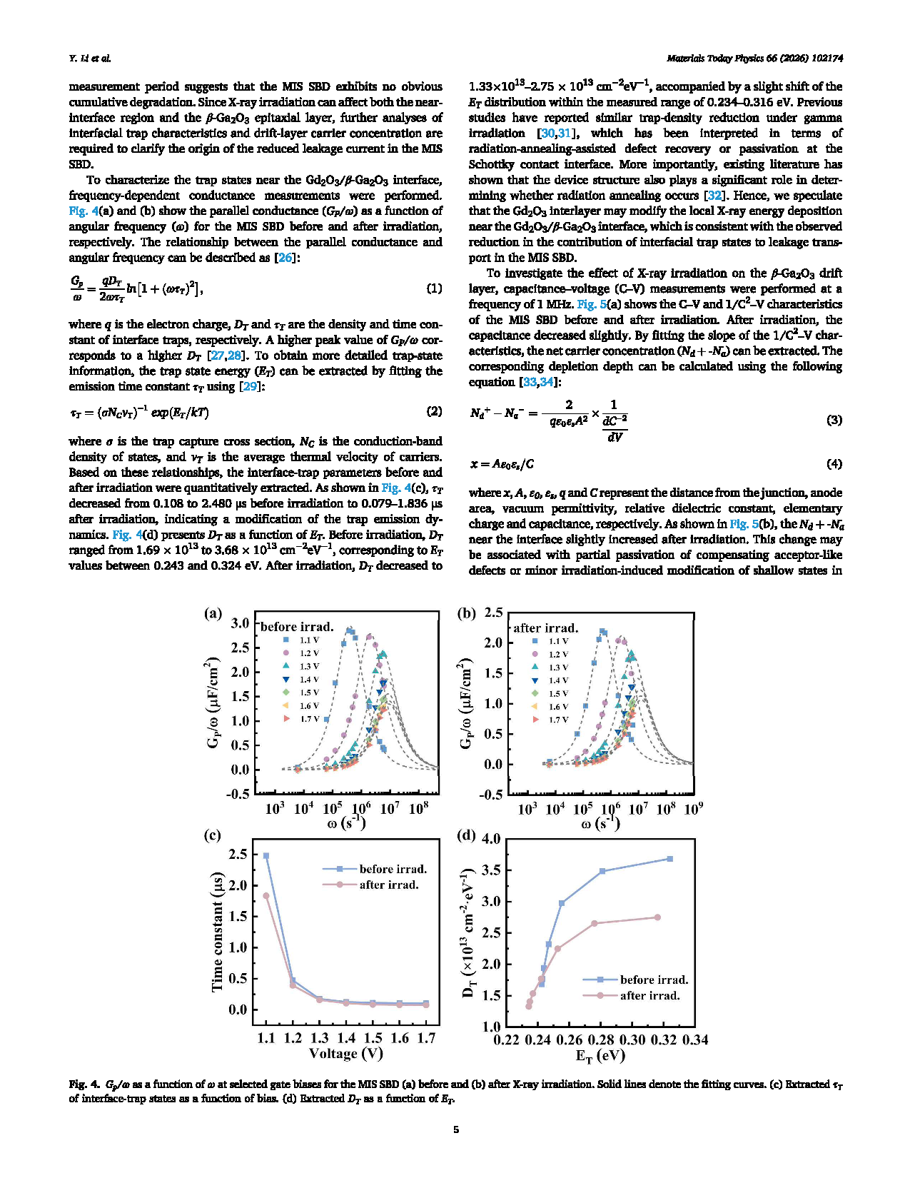
Fig. 4. Gp/ω as a function of ω at selected gate biases for the MIS SBD (a) before and (b) after X-ray irradiation. Solid lines denote the fitting curves. (c) Extracted τT of interface-trap states as a function of bias. (d) Extracted DT as a function of ET.
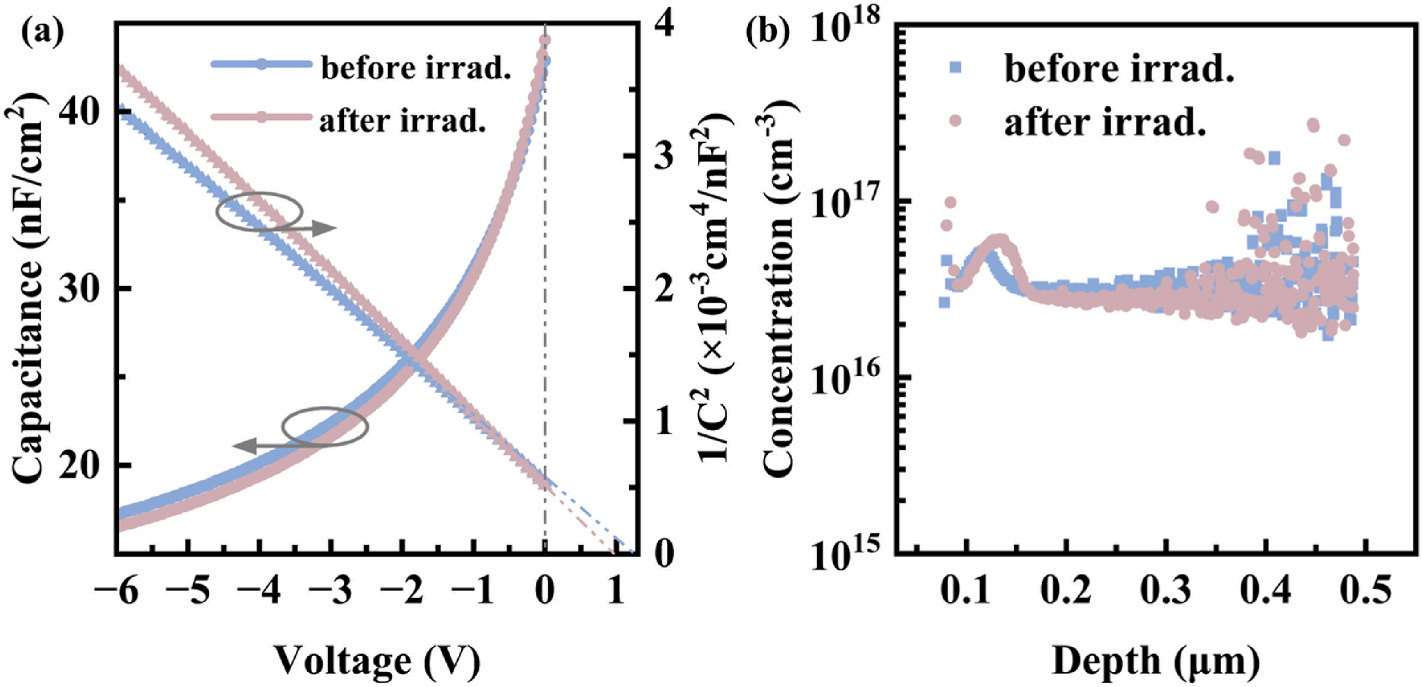
Fig. 5. (a) C-V and 1/C²-V plot of the MIS SBD measured at room temperature before and after X-ray irradiation. (b) Extracted carrier concentration depth profile in the β-Ga₂O₃ drift layer of the MIS SBD before and after irradiation.
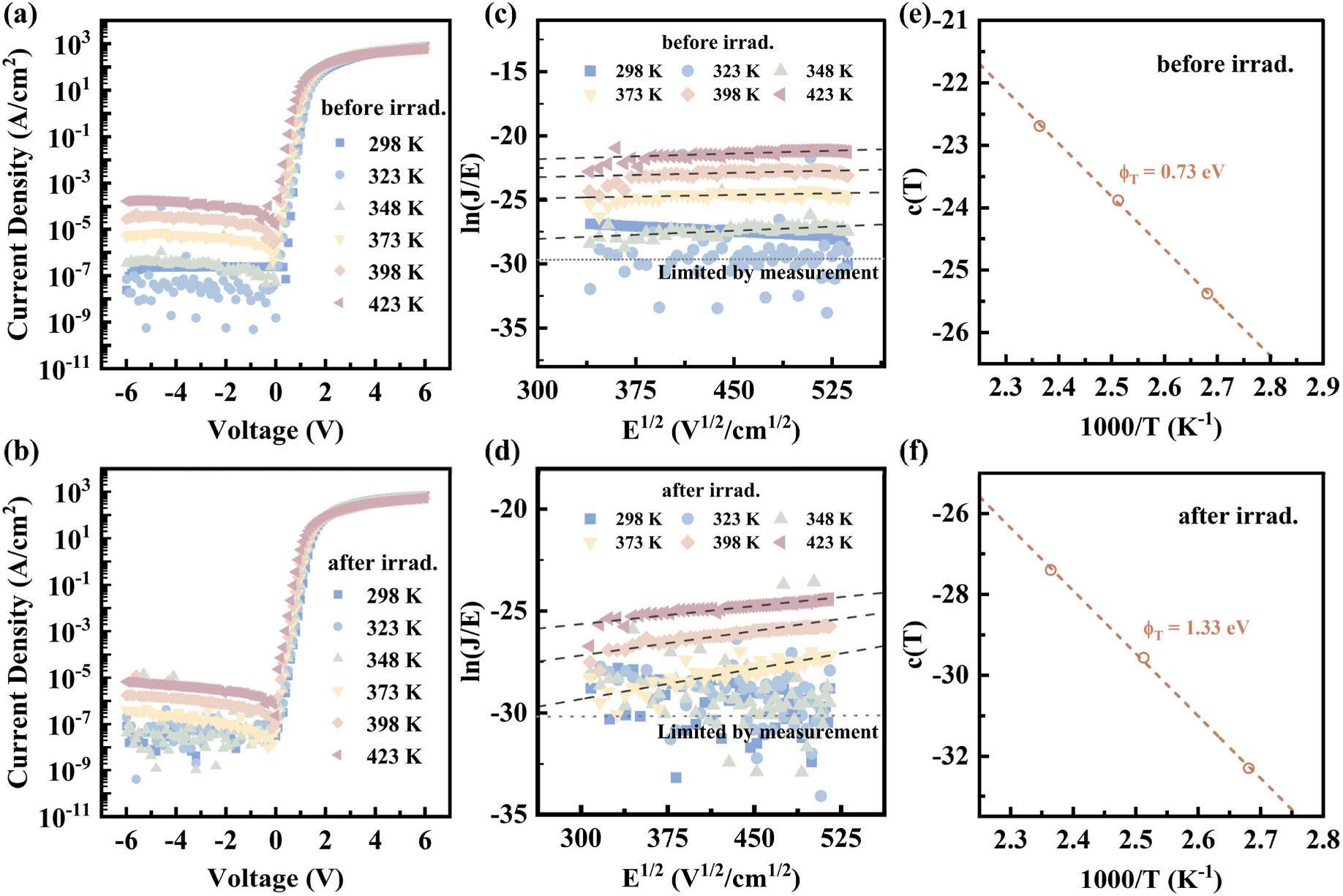
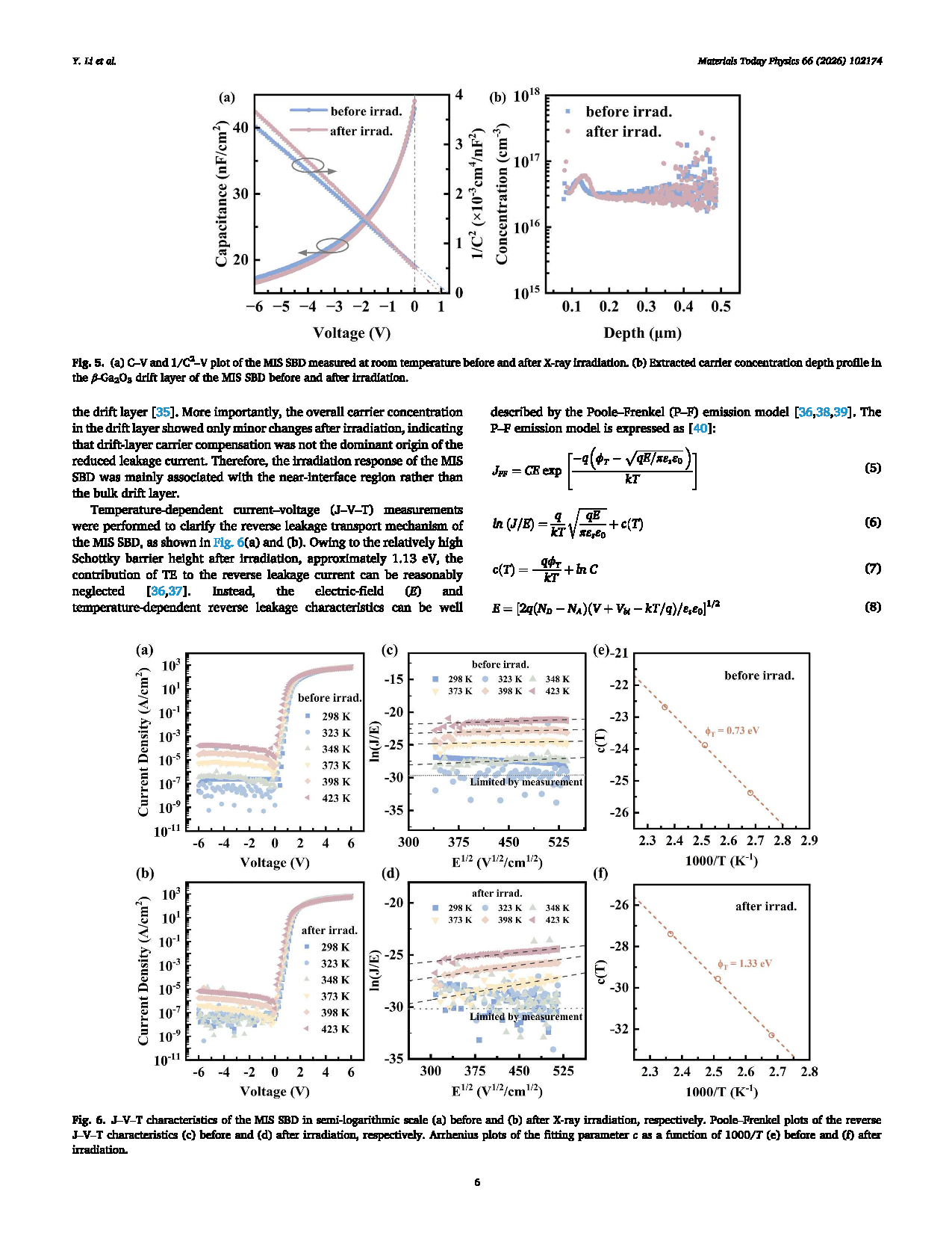
Fig. 6. J-V-T characteristics of the MIS SBD in semi-logarithmic scale (a) before and (b) after X-ray irradiation, respectively. Poole-Frenkel plots of the reverse J-V-T characteristics (c) before and (d) after irradiation, respectively. Arrhenius plots of the fitting parameter c as a function of 1000/T (e) before and (f) after irradiation.
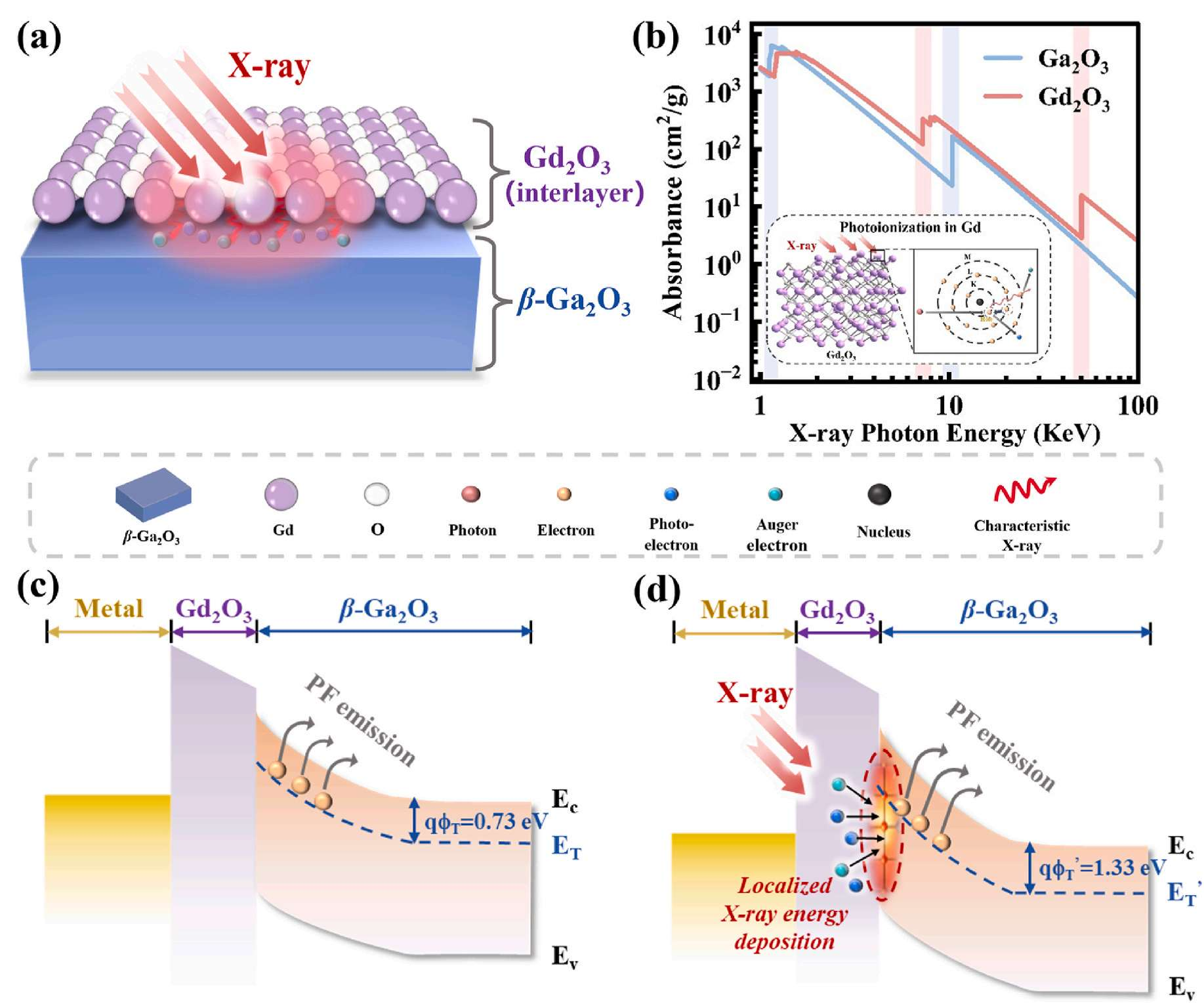
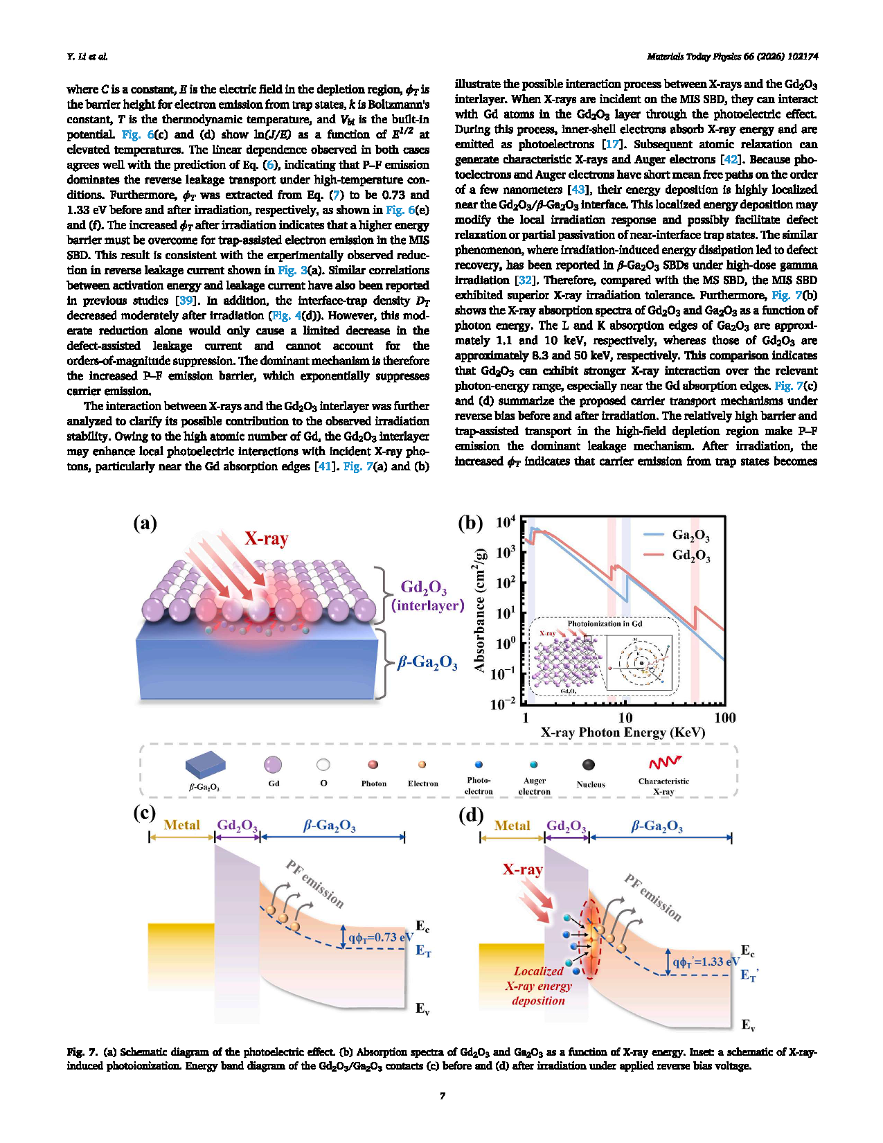
Fig. 7. (a) Schematic diagram of the photoelectric effect. (b) Absorption spectra of Gd₂O₃ and Ga₂O₃ as a function of X-ray energy. Inset: a schematic of X-ray-induced photoionization. Energy band diagram of the Gd₂O₃ / Ga₂O₃ contacts (c) before and (d) after irradiation under applied reverse bias voltage.
DOI:
doi.org/10.1016/j.mtphys.2026.102174
Instruction
Official Account

Cooperation
Top
