


Positioned as the functional “waist” in Hangzhou’s integrated urban development layout, Fuyang has further rolled out its local “Dual Excellence” Initiative this year. An upsurge of hard work is sweeping all industries, with countless dedicated strivers standing firm at their posts and charging ahead in pursuit of progress.
Starting today, the Office of the District Leading Group for the “Double First-Class” Initiative, in collaboration with the Fuyang District Media Center, is launching the series report “Strengthening the Waist and Striving for Excellence · Saluting the Strivers.” The series highlights frontline pioneers who have made sustained contributions to technological innovation, industrial breakthroughs, rural common prosperity, and public service development. Through their stories of overcoming challenges, the series aims to reveal the driving force behind Fuyang’s pursuit of excellence and showcase the upward momentum and hardworking spirit of a city striving for continuous growth.
Featured in the first issue:
Carrying a Gallium mission in his heart, Qi Hongji has put down roots in Fuyang to pioneer fourth-generation semiconductor technology.
Shouldering dual missions, advancing scientific research and entrepreneurship in parallel.
Qi Hongji, a second-level research fellow at the Shanghai Institute of Optics and Fine Mechanics, Chinese Academy of Sciences, is a renowned expert in the field of optoelectronic functional crystals in China. He currently serves as the Director of the Hangzhou Institute of Optical Precision Machinery (hereinafter referred to as “Hangzhou Institute of Optics”) and Chairman of Hangzhou Fujia Gallium Technology Co., Ltd. (hereinafter referred to as “Fujia Gallium”). While undertaking major national scientific research projects in nonlinear optical crystals, he also shoulders the responsibility of incubating and commercializing research achievements through a national-level excellence incubator platform.
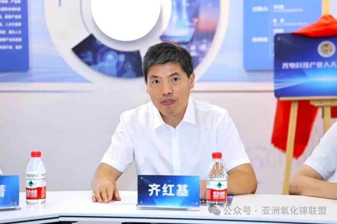
△Photo by Chen Heng
On this fertile land of hope in Fuyang, he has been dedicated to building Hangzhou Institute of Optical Precision Machinery’s technology commercialization platform while leading his team in tackling key “bottleneck” challenges across the entire gallium oxide industry chain.
With more than two decades of scientific research experience and the resilience of a pioneer, he has led his team in developing the world’s first 12-inch gallium oxide single crystal, advancing the integration of the entire gallium oxide value chain from substrates and epitaxy to devices and applications. He also led the drafting of the first national standard in the field of gallium oxide. Through relentless efforts, he has established a new foundation for the ultra-wide-bandgap semiconductor industry in the Fuchun River region, delivering an inspiring achievement report of scientific innovation through action and dedication.
Pioneering Cross-Disciplinary Innovation
Rooted in Fuyang’s Frontline of Scientific and Technological Advancement
Fujia Gallium is the first company incubated by the Hangzhou Institute of Optical Precision Machinery. Entering the temperature-controlled, ultra-clean production workshop, crystal growth equipment operates efficiently as gallium oxide powders are melted at temperatures of 1,800°C and precisely grown into high-quality single crystals under controlled conditions. Operators simply touch the screen to reveal the “Fuyang standard” of advanced material manufacturing.
As a national high-tech enterprise dedicated to the industrialization of the ultra-wide-bandgap semiconductor material gallium oxide, Fujia Gallium achieved the world’s first successful preparation of a 12-inch gallium oxide single crystal in March this year, setting a new global record and becoming the first company worldwide to master growth technology for gallium oxide crystals of this size.
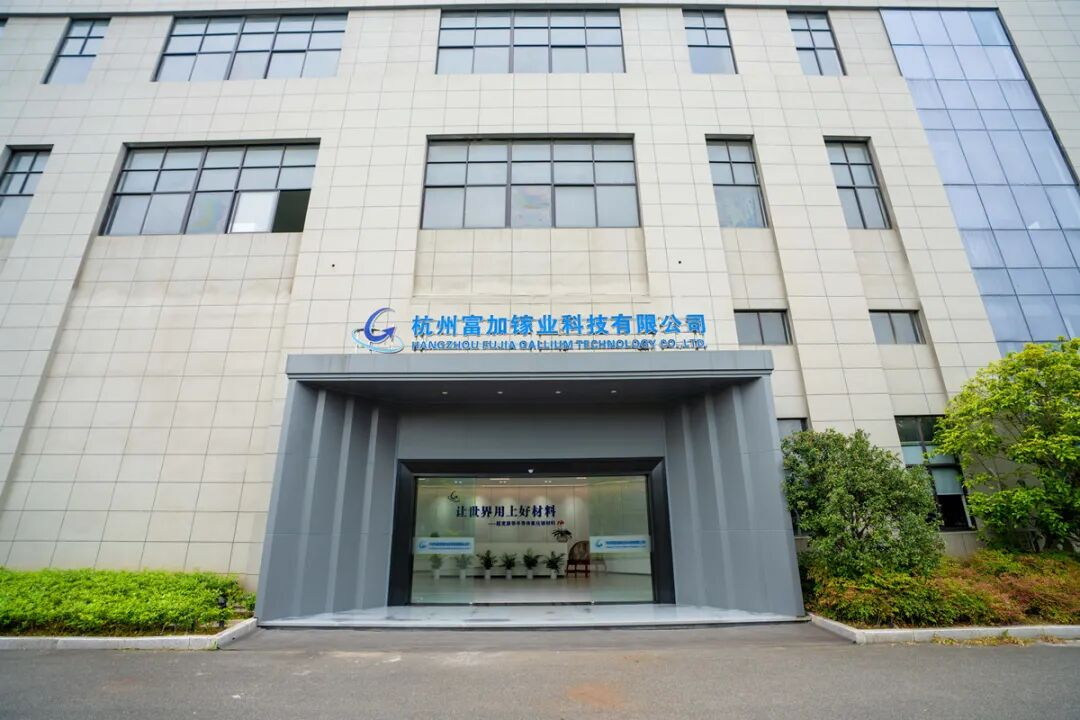
△Photo by Jin Fei
It is hard to imagine that when the project was first introduced to Fuyang in 2019, the team only possessed 2-inch gallium oxide crystal growth technology, leaving a significant gap before reaching the 6-inch substrate scale required for industrialization. At that time, China’s gallium oxide industry chain was almost nonexistent, with few companies involved in epitaxy and device development. High-end substrate materials were long dominated by enterprises from the United States and Japan, which imposed export restrictions on China.
When Qi Hongji first learned that the gallium oxide project would be launched in Fuyang, he was filled with concerns.
“Honestly, I was not very optimistic about this project at the beginning,” he said. “The technology was still at an early stage of maturity. We could only produce 2-inch crystals, which could not meet the requirements of industrial production lines. Moreover, the entire industrial chain was fragmented. There were almost no mature supporting companies covering upstream single crystals, midstream epitaxy, and downstream devices. Simply focusing on materials could easily lead to a dilemma where ‘products accumulate in warehouses without practical applications.’”
A long-term vision from Zhang Long, then Deputy Director of the Shanghai Institute of Optics and Fine Mechanics, Chinese Academy of Sciences, and founder of the Hangzhou Institute of Optical Precision Machinery, completely dispelled his concerns.
“At that time, Deputy Director Zhang told me that our goal was not to build a company focused on short-term profits, but to create a benchmark enterprise with industry-leading influence and long-term value,” Qi Hongji recalled.
Qi Hongji explained that gallium oxide is a strategic material with both military and civilian applications. Even if the civilian market had not yet reached explosive growth in the short term, key national sectors would still require an independent and controllable supply of such materials. Therefore, it was necessary to make early investments and establish a new foundation for domestically developed semiconductor materials.
Driven by this mission of advancing critical technologies for the nation, he took on the challenge and embarked on a pioneering journey in Fuyang.
Targeting a Strategic Frontier
Advancing the Ga₂O₃ Full Industrial Chain Despite Challenges
In China’s “15th Five-Year Plan,” gallium oxide (Ga₂O₃) has been identified as one of the key industrial directions for future breakthroughs.
“Gallium oxide combines two major advantages: high performance and low cost, making it a fundamental material for power devices used in new energy vehicles, photovoltaic energy storage systems, and power grids,” said Qi Hongji. “China’s new energy industry has achieved global leadership in scale, and its power device market accounts for nearly half of the global market. Under the national energy security strategy, domestically controllable gallium oxide materials hold tremendous application potential.”
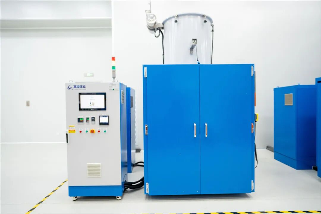
△ Production workshop of Fujia Gallium (Photo by journalist Jin Fei)
However, focusing solely on single-crystal substrates cannot activate the industrial ecosystem. Breaks between upstream and downstream sectors would prevent cutting-edge technologies from realizing their application value. After careful consideration, Qi Hongji made a relatively uncommon strategic decision in the industry: relying on the support of the Hangzhou Institute of Optical and Precision Mechanical Research, the team independently established an epitaxy R&D and production team to achieve full integration across the upstream and downstream Ga₂O₃ industry chain.
Qi Hongji explained the underlying logic behind developing epitaxy capabilities in-house: “Our internally produced single crystals can directly supply the epitaxy team, eliminating external procurement costs while enabling faster technological iteration and more comprehensive feedback. Meanwhile, we already possess practical experience in industrialization, allowing us to directly transfer the mature mass-production principles of single crystals to epitaxial processes, significantly accelerating R&D and optimization.”
This internal collaborative model has delivered remarkable results. The performance of the team’s epitaxial wafers has rapidly reached the level of international leaders and has successfully passed validation by downstream customers.
Currently, MOSFET devices developed by Jiufengshan Laboratory based on epitaxial wafers supplied by Fujia Gallium have achieved a breakdown voltage exceeding 9000 V, setting a new world record for Ga₂O₃ voltage endurance. In addition, the phonon-assisted absorption Ga₂O₃ photoconductive switch jointly developed under the leadership of Sun Yat-sen University with deep participation from Fujia Gallium has achieved a voltage conversion efficiency of 98.9%.
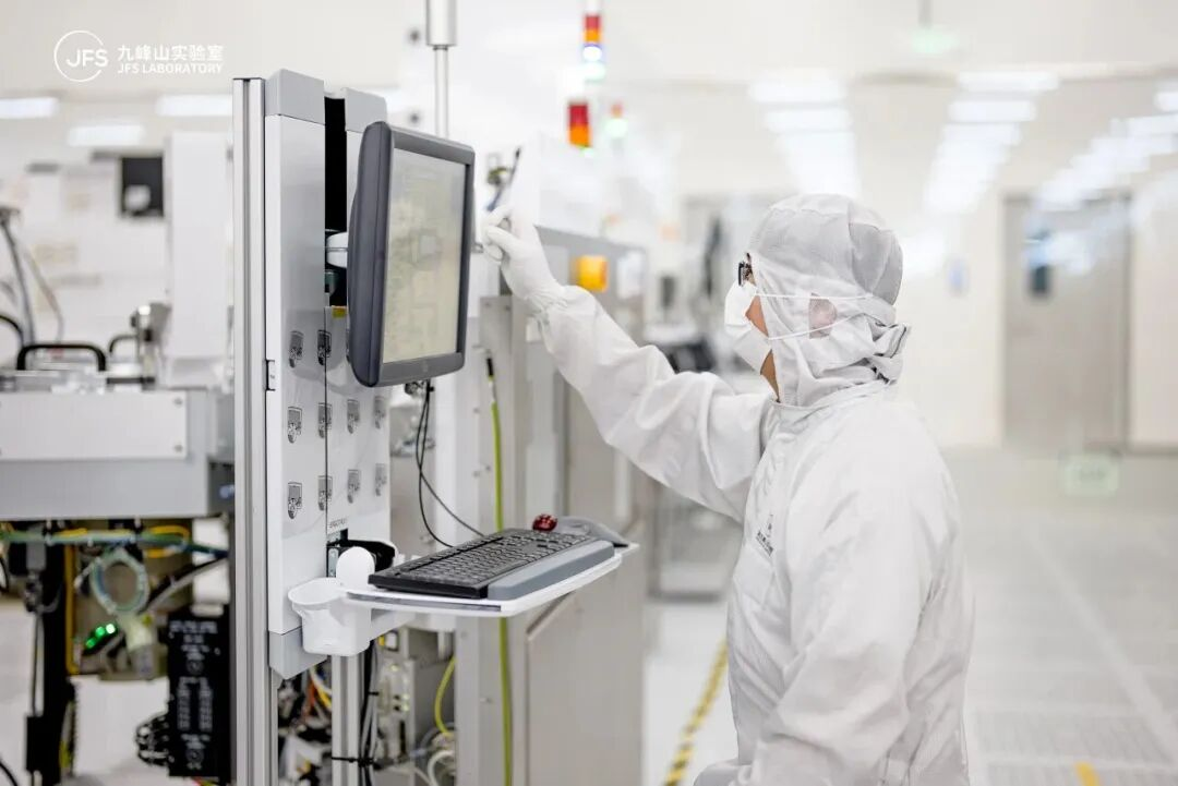
△ Jiufengshan Laboratory in Wuhan, Hubei, China
After the preliminary validation of device performance, application-side verification became the next major challenge. In China, few companies were willing to invest substantial resources in developing module systems based on gallium oxide power devices, let alone conducting practical application validation under real-world operating conditions. Under these circumstances, while collaborating with downstream research teams and enterprises on device development, Fujia Gallium jointly worked with Shanghai Gongcheng Semiconductor Technology Co., Ltd. to carry out full-chain collaborative research and development covering “materials–devices–applications” around key technologies for gallium oxide industrialization. The gallium oxide diode devices jointly developed by the two parties have successfully passed chip-level testing and packaging processes, enabling the validation of gallium oxide devices in liquid-cooling modules.
Fujia Gallium is leading the drafting of the first national standard in the field of gallium oxide, holding dozens of domestic and international invention patents and providing technical support and material solutions for numerous research institutes and enterprises across China. Meanwhile, the company has taken the lead in organizing industry events such as the Cross-Strait Symposium on Gallium Oxide Materials and Devices and the Andingshan Forum, promoted the establishment and registration of the Asian Gallium Oxide Alliance, and continued to build an industry-wide technology exchange platform as a leading enterprise, accelerating ecosystem development in the gallium oxide field.
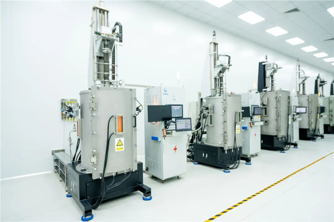
△ Fujia Gallium production workshop (Photo by reporter Jin Fei)
Cultivating an In-House Talent Pipeline
Building a Foundation for Long-Term Growth
Talent is the cornerstone of hard-tech development. In team building, Qi Hongji emphasizes both talent recruitment and internal cultivation, while highlighting the importance of self-driven learning capabilities. He frankly notes that compared with hiring external executives at high salaries, locally cultivated teams tend to have stronger loyalty, greater sense of responsibility, and deeper familiarity with business processes, effectively avoiding risks such as poor adaptation of external talent and imbalanced compensation structures.
“This team has exceptional learning capabilities, with each member capable of handling multiple roles. They are the foundation for the company’s long-term development.” When talking about his team, Qi Hongji speaks with great pride.
Looking ahead, he has a clear vision and strategic plan for the future—
“In the short term, we will continue advancing the construction of 6-inch and 8-inch gallium oxide substrate and epitaxial wafer production capacity, targeting an annual output of tens of thousands of wafers. We aim to provide downstream device customers with high-quality, large-size epitaxial wafers, accelerate device packaging, testing, and reliability validation, and actively promote demonstration applications in areas such as new energy charging infrastructure and industrial power supplies. We strive to achieve significant revenue growth in the coming years.
In the long term, we will continue improving the quality of gallium oxide epitaxial wafers, further explore the potential of gallium oxide materials, and reduce material costs through technological breakthroughs. By accelerating the deployment of gallium oxide devices in high-voltage and ultra-high-voltage applications—including solid-state transformers (SSTs) for AI servers, rail transit, and national power grid systems—we aim to realize our vision of ‘providing the world with high-quality materials,’” said Qi Hongji.
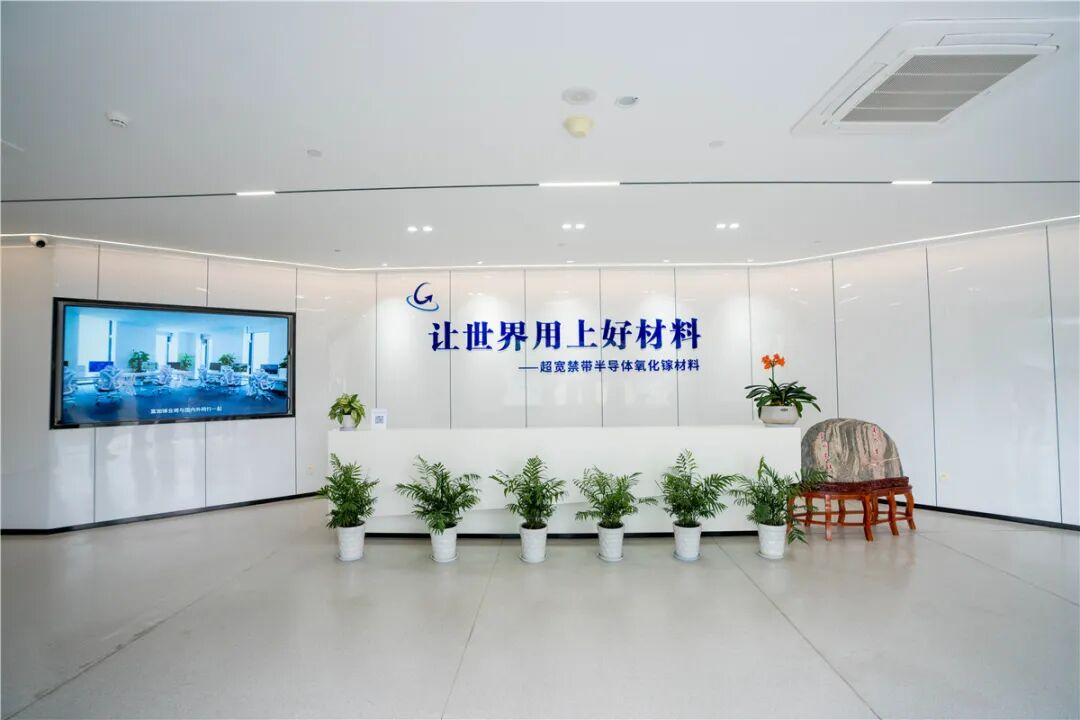
△ Photo by reporter Jin Fei.
Leveraging the Strong Foundation of Hangzhou Institute of Optics and Precision Mechanics
Building a Science and Innovation Hub in Fuyang
The growth of Fujia Gallium has been inseparable from the comprehensive support and cultivation provided by the Hangzhou Institute of Optics and Precision Mechanics.
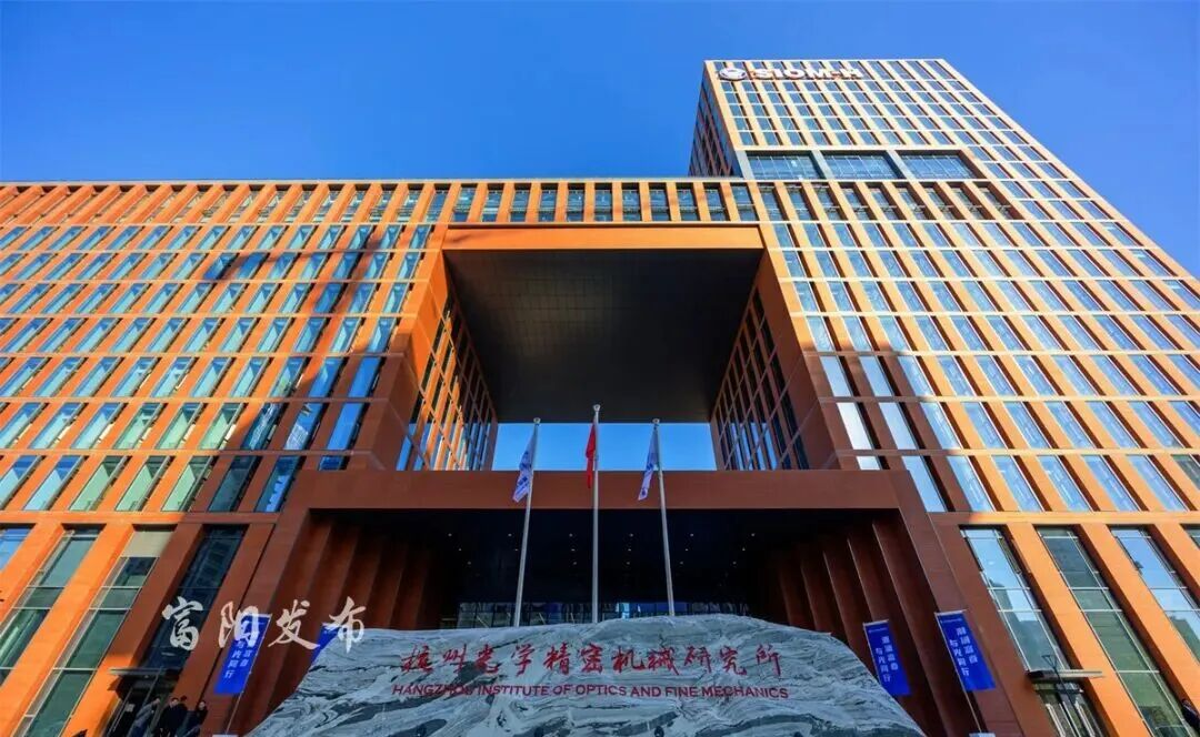
△ Hangzhou Institute of Optics and Precision Mechanics (Photo by Zhu Xiaochen)
Since Fujia Gallium was officially established in 2019, the Hangzhou Institute of Optics and Precision Mechanics has innovatively participated in the company’s development as an “entrepreneurial partner.”
“During the early stage of entrepreneurship, the most challenging issues, including funding, finance, legal affairs, and talent recruitment, were gradually resolved with the support of the Hangzhou Institute of Optics and Precision Mechanics platform.” Qi Hongji highlighted the comprehensive support provided by the platform.
The Hangzhou Institute of Optics and Precision Mechanics has established a professional, modular, standardized, and customized full-chain incubation service system, precisely covering key areas urgently needed by scientists during commercialization, including technology application scenario exploration, product development, intellectual property strategy, financial and legal compliance, core team building, government resource coordination, follow-on financing support, market expansion, and corporate governance optimization.
Meanwhile, through the China Optics Valley (Zhongke Shengu Guang) Science and Innovation CEO Training Program, the institute provides entrepreneurship training for scientists, helping them transform from “scientists” into outstanding “entrepreneurs.”
As a “new Fuyang resident,” Qi Hongji has developed a strong sense of belonging to this land after six years of deep commitment.
“Fuyang’s business environment is truly supportive and inspiring. Government departments provide strong support for hard-tech enterprises, and whenever there is a need for industrial development, relevant policies and supporting services are promptly put in place,” he praised.

△ Hangzhou Fuchun Bay New City (Photo by Zhu Xiaochen)
Anchored in Fuyang’s strategic positioning as the “waist” of Hangzhou’s integrated urban development and at a pivotal stage of advancing the “Double First-Class” initiative, Qi Hongji believes that advanced materials represent a key pathway for Fuyang’s industrial transformation. Local research platforms and hard-tech enterprises shoulder the important mission of strengthening weak links in the semiconductor industry chain.
“Fuyang has established a comprehensive support system for technology commercialization and offers an excellent business environment, making it fertile ground for hard-tech entrepreneurs,” he said. “There are never shortcuts in scientific innovation or industrial development. Only by staying committed for the long term, confronting technological bottlenecks and industrial gaps head-on, and forging a path through challenges can we overcome critical ‘bottleneck’ obstacles.”
He hopes that innovators and entrepreneurs from all sectors will remain true to their original aspirations, take root in the Fuchun landscape, continue tackling challenges through practical efforts, and jointly build the innovation backbone supporting Fuyang’s high-quality development.
Instruction
Official Account

Cooperation
Top
