


Researchers from Chongqing Normal University, Northeast Normal University, University of Electronic Science and Technology of China and the University of Wollongong have published a paper titled “Interface-Defect Synergy Engineering of Amorphous Ga₂O₃ for Voltage-Tunable Dual-Mode Optoelectronic Devices: Self-Powered Imaging and Neuromorphic Vision” in the academic journal Advanced Functional Materials.
Background
Traditional von Neumann architecture physically separates photodetection, memory and computing units, leading to high data transmission latency and excessive power consumption, which limits lightweight intelligent vision hardware. Integrating photoelectric sensing and synaptic cognitive functions into a single device is a core route to break computing bottlenecks, yet the two functions have contradictory demands on carrier regulation: high-sensitivity detection requires efficient carrier separation, while synaptic behavior relies on charge trapping to realize gradual conductance modulation, which is hard to balance simultaneously. Most existing dual-mode devices adopt multi-heterojunction composite structures with difficult band offset control, complex fabrication and uncontrollable interface defects. Amorphous Ga₂O₃ owns an ultra-wide bandgap and can be fabricated in large area at low cost, making it a candidate for solar-blind detection, while controllable interface defect regulation schemes are still absent. This work proposes an interface-defect synergy engineering strategy. In vertical ITO/GaOₓ/Al architecture, oxygen vacancies and asymmetric potential barriers are precisely introduced via in-situ interfacial redox reactions. Only a single active layer is adopted to realize two voltage-switchable working modes: zero-bias self-powered solar-blind imaging and low-power synaptic response, balancing high-sensitivity weak light detection and low-power learning-memory behavior, and offering a simple feasible solution for monolithic integrated intelligent vision hardware.
Abstract
Integrating disparate optoelectronic functionalities—ranging from self-powered photodetection to neuromorphic computing— within a unified, single-material architecture is pivotal for the next generation of bias-programmable intelligent vision systems. Here, we report a voltage-tunable, monolithic platform based on amorphous GaOₓ (ITO/GaOₓ/Al) that achieves bias-programmable dual-mode operation, uniting self-powered solar-blind photodetection with low-power optoelectronic synaptic functionalities. The dual-modality originates from the synergistic coupling between asymmetric interfacial potential barriers and oxygen-vacancy engineering, which is in situ induced by interfacial redox reactions at the GaOₓ/Al junction. Benefiting from this precise interface-defect co-engineering, the device exhibits exceptional self-powered solar-blind detection with high responsivity, a rapid response of ∼100 µs, and a detection limit down to 13 nW. Under a low bias, it emulates bio-realistic synaptic dynamics—including paired-pulse facilitation and learning–forgetting–relearning processes—with an ultralow energy footprint of 18 pJ. Reversible voltage modulation enables both single-pixel and 10 × 10 array devices to bridge the gap between high-contrast transient imaging and long-term visual memory. Moreover, a neuromorphic visual system constructed from this platform performs robust “detection–storage–recognition” tasks even under external noise. This study establishes a transformative route for bias-programmable optoelectronic integration, effectively uniting sensing and cognitive functions within a simplified, high-performance single-material system.
Highlights
① An original interface-defect synergy engineering strategy for amorphous GaOₓ is proposed. Oxygen vacancies are generated via in-situ redox at Al interface, and dual voltage-switchable modes are realized with only one active layer without multi-heterostructure;
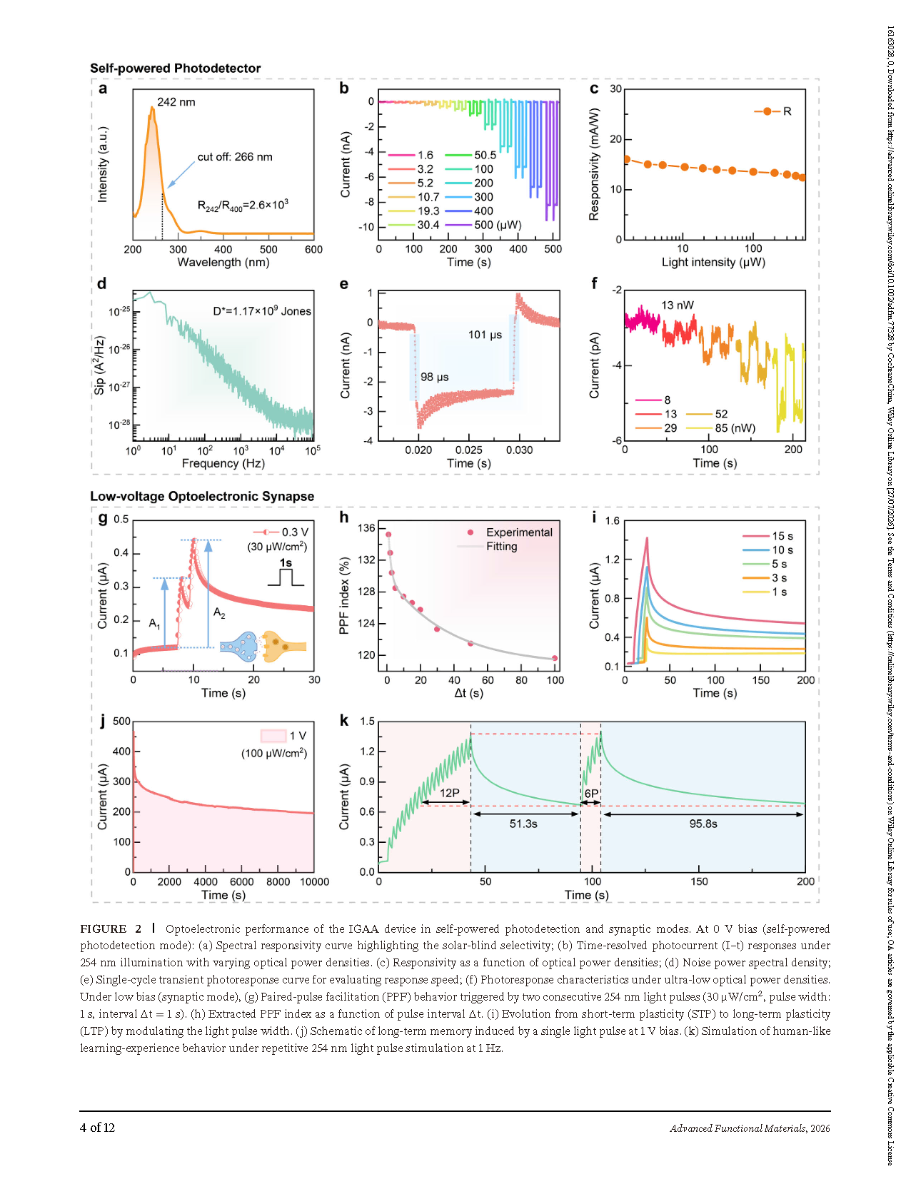
② Under zero-bias self-powered mode, the device achieves an ultra-weak detection limit of 13 nW, response time around 100 µs, and solar-blind/visible rejection ratio up to 2.6 × 10³;
③ Under low bias, the device accurately emulates biological synaptic behaviors including paired-pulse facilitation, short/long-term plasticity and learning-forgetting process, with ultra-low energy consumption of 18 pJ per synaptic event;
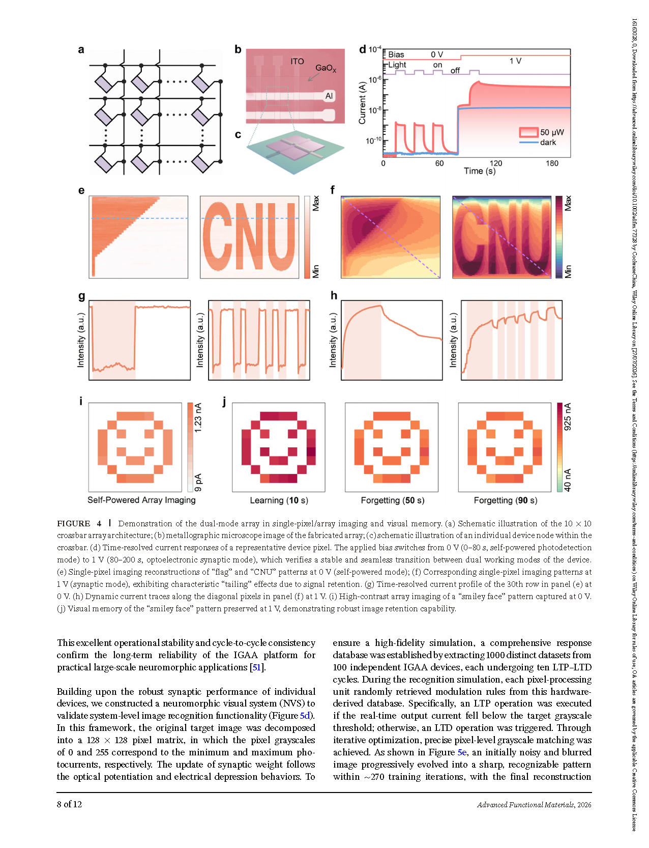
④ A 10 × 10 crossbar array is fabricated, which can separately realize high-contrast self-powered solar-blind imaging and long-term image memory retention;
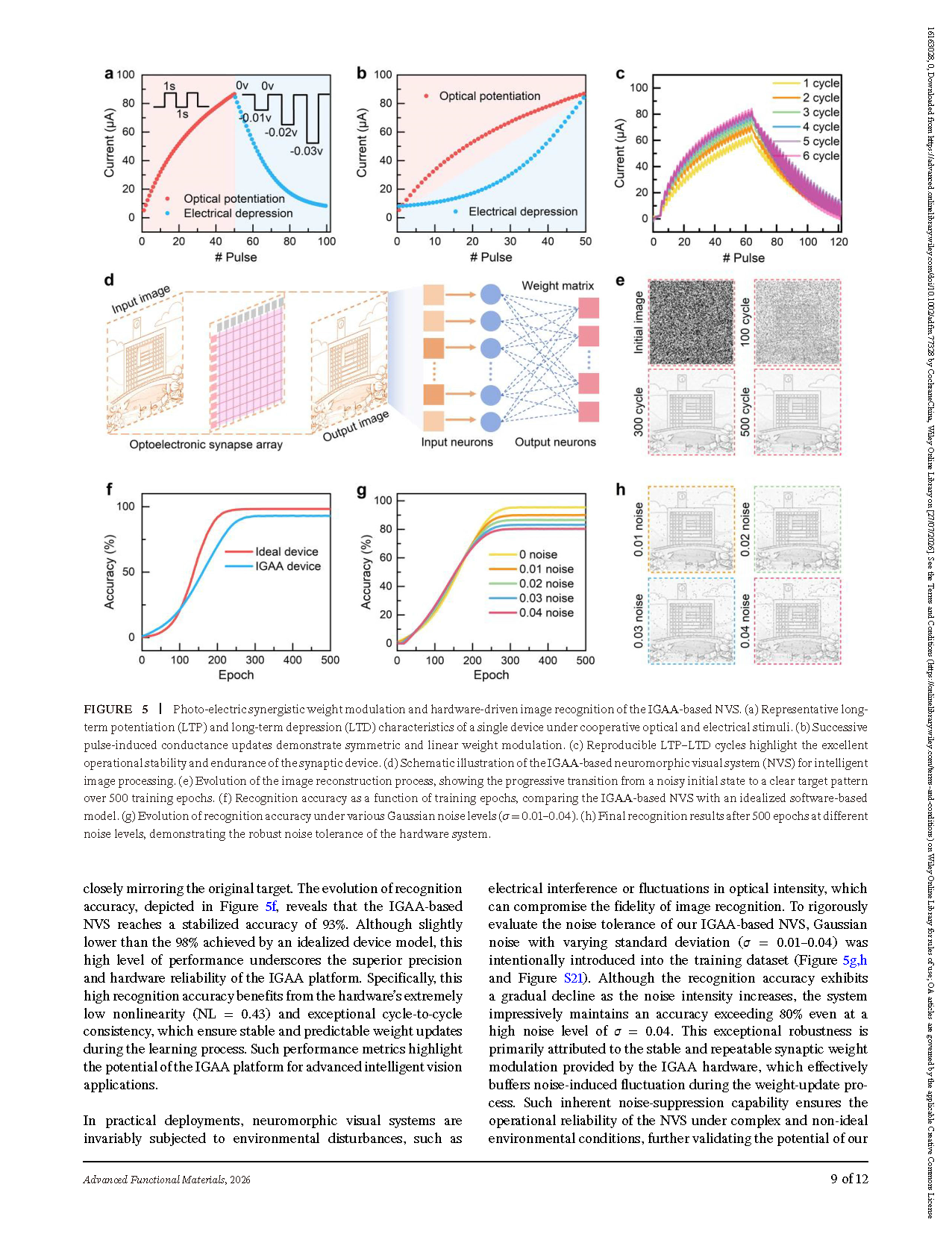
⑤ A neuromorphic visual system is constructed, which stably completes image detection, storage and recognition even under noise disturbance with stable recognition accuracy of 93%.
Working Mechanism
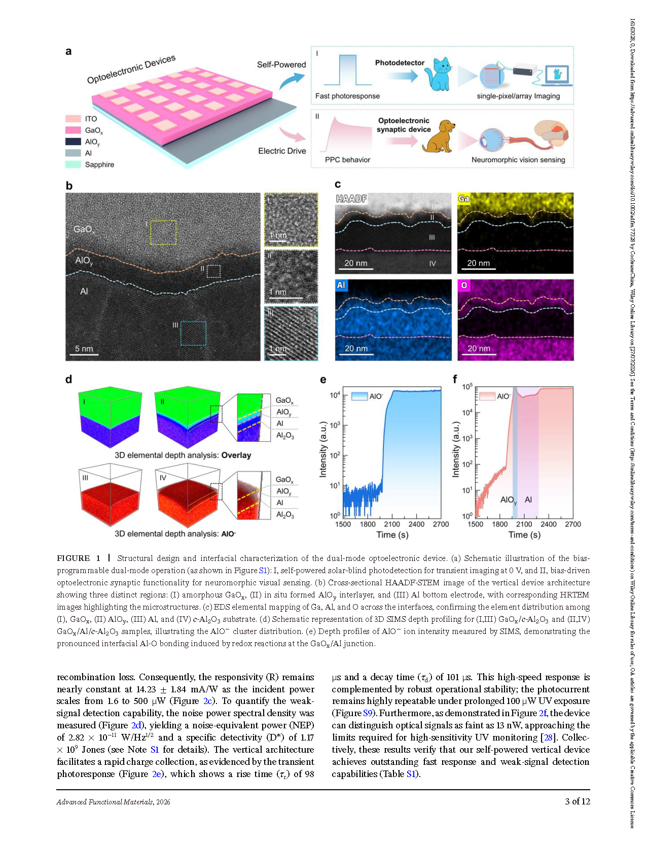
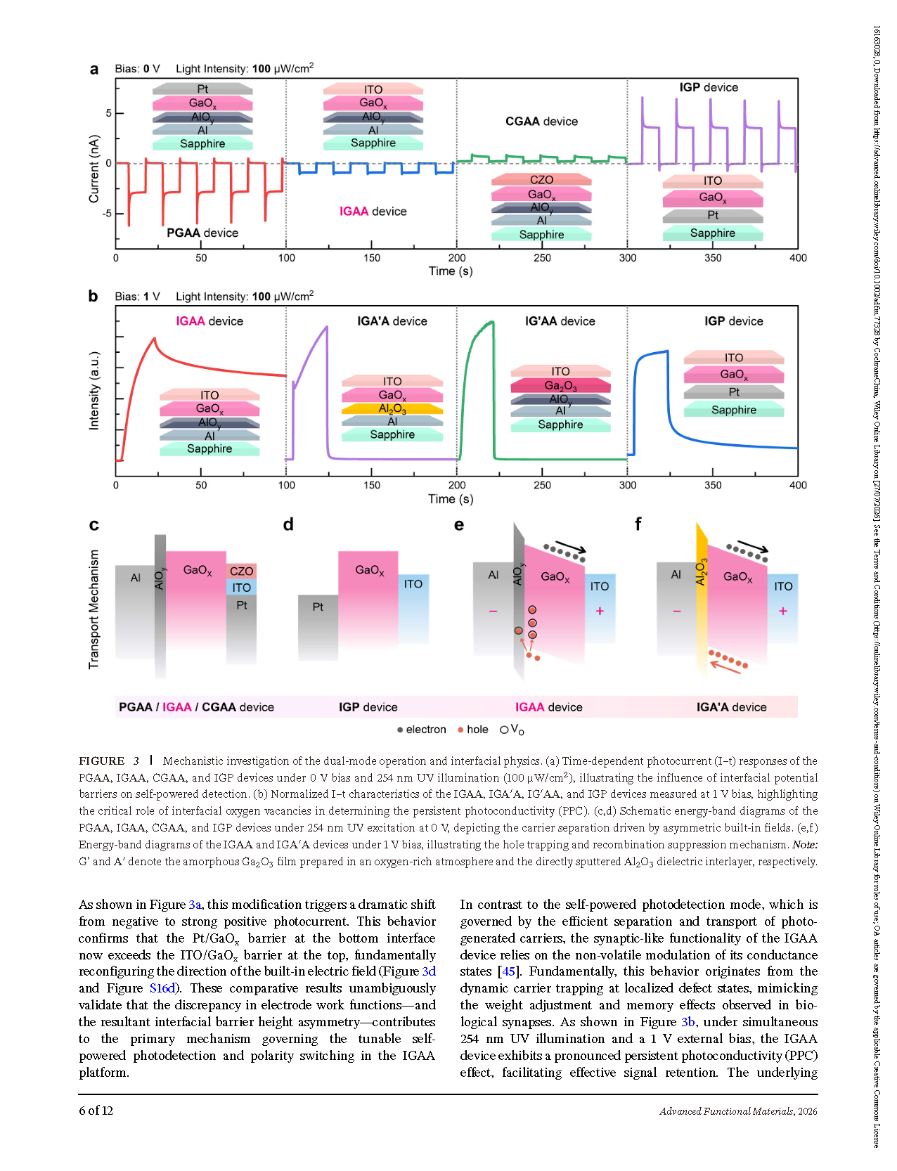
To elucidate the mechanism underlying the dual-mode operation, the researchers further constructed a series of control devices for systematic verification. The results demonstrate that variations in interfacial potential barriers induced by different electrode configurations determine the direction of photogenerated carrier separation under zero bias, enabling self-powered photoelectric conversion. Meanwhile, oxygen vacancies generated at the Al/GaOₓ interface act as carrier trapping centers, inducing persistent photoconductivity under low bias and thereby enabling synaptic memory functionality. These findings clearly distinguish the distinct roles of interfacial barriers and defect states in the two operating modes, providing a physical basis for voltage-programmable multifunctional optoelectronic integration.
Conclusion
In summary, we have developed a voltage-tunable, vertical optoelectronic device based on a single amorphous Ga₂O₃ layer to realize bias-programmable dual-mode operation within a monolithic system. By leveraging an interface-defect co-engineering strategy, the synergistic coupling between asymmetric interfacial potential barriers and oxygen-vacancy modulation enables the seamless reconfiguration of the device between self-powered solar-blind photodetection and low-power optoelectronic synaptic functionalities. Benefiting from this heterojunction-free architecture, the platform exhibits exceptional sensing performance, including high responsivity, a rapid response time of ∼100 µs, and ultraweak signal detection limits down to 13 nW. Simultaneously, the device emulates energy-efficient synaptic plasticity with a lower power consumption of 18 pJ per event and superior operational stability. This implementation of voltage modulation facilitates the transition from high-contrast transient imaging to persistent visual memory in both single-pixel and array configurations, effectively bridging the functional gap between signal acquisition and neuromorphic perception. This work not only establishes a streamlined, single-material route toward multifunctional optoelectronic integration but also provides a robust hardware foundation for the development of energy-efficient, intelligent optoelectronic systems for future cognitive photonics, neuromorphic visual networks, and large-scale integrated hardware vision systems.
Project Support
The authors gratefully acknowledge support from the National Natural Science Foundation of China (Grant Nos. 62574029 and 12304102), the Natural Science Foundation of Chongqing (Grant Number CSTB2023NSCQ-MSX0479), the Science and Technology Research Project of Chongqing Municipal Education Commission (Grant Nos. KJZD-M202600502, KJQN202300536 and KJQN202400558) and the Chongqing Normal University Foundation (Grant Nos. 23XLB029, 23XLB002, and S202510637007).
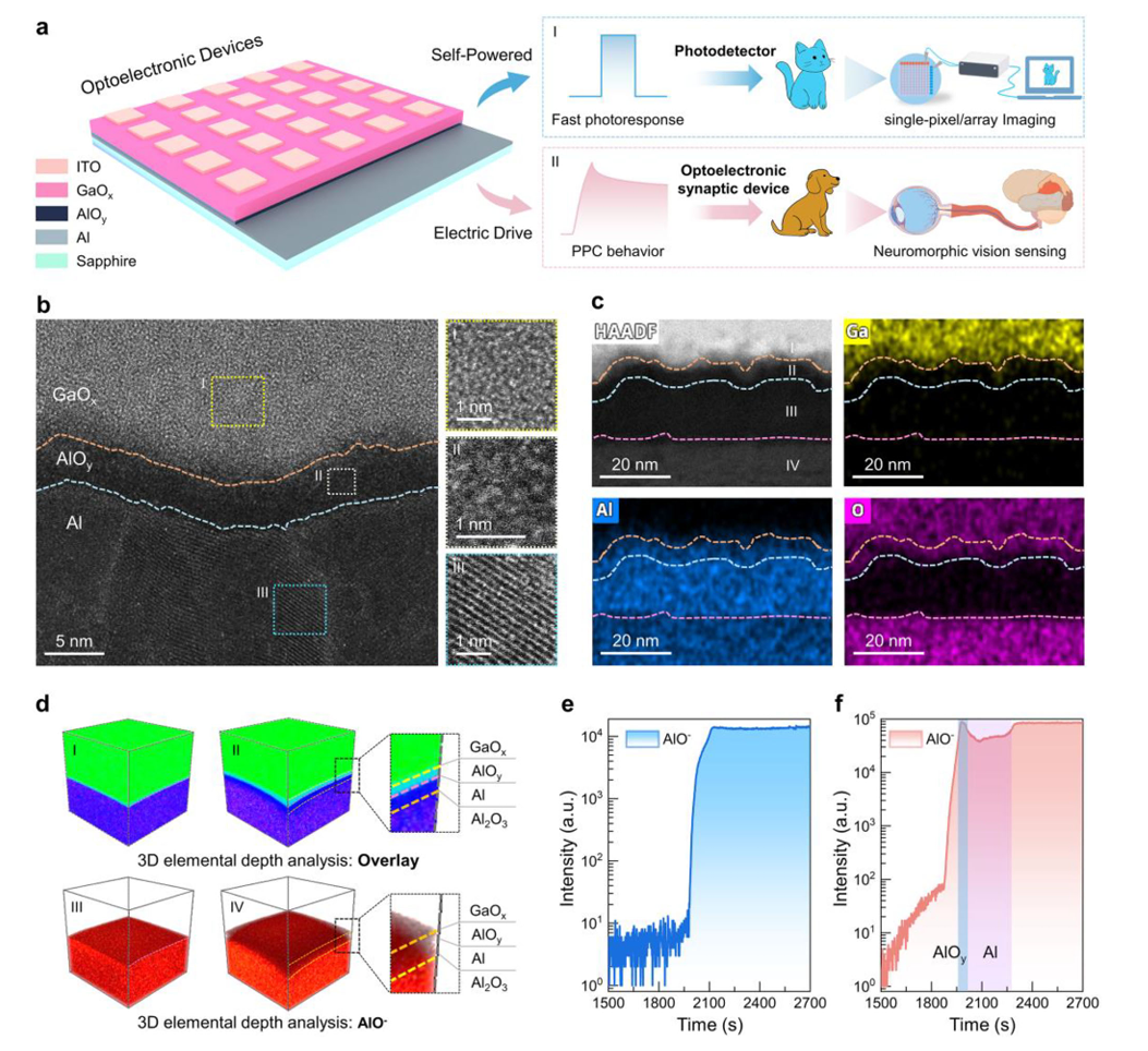
Figure 1 (a) Schematic diagram of dual-mode device array, marking two working modes: zero-bias self-powered imaging and low-voltage neuromorphic vision; (b) Cross-sectional HAADF-STEM image of the device, divided into amorphous GaOₓ, in-situ formed AlOᵧ interlayer and Al bottom electrode regions; (c) EDS elemental mapping of Ga, Al and O across interfaces; (d) Schematic of 3D SIMS depth profiling for GaOₓ/c-Al₂O₃ and GaOₓ/Al samples; (e,f) Depth profiles of AlO⁻ ion intensity for two samples, verifying oxygen-vacancy-rich layer generated by interfacial redox reaction
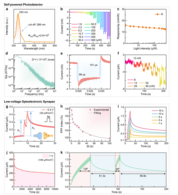
Figure 2 Optoelectronic performance of the IGAA device in self-powered photodetection and synaptic modes. At 0 V bias (self-powered photodetection mode): (a) Spectral responsivity curve; (b) Time-resolved photocurrent responses under 254 nm illumination with varying optical power densities; (c) Responsivity as a function of optical power densities; (d) Noise power spectral density; (e) Single-cycle transient photoresponse curve for evaluating response speed; (f) Photoresponse characteristics under ultra-low optical power densities. Under low bias (synaptic mode), (g) Paired-pulse facilitation behavior triggered by two consecutive 254 nm light pulses with interval Δt = 1 s; (h) Extracted PPF index as a function of pulse interval Δt; (i) Evolution from short-term plasticity to long-term plasticity by modulating the light pulse width; (j) Schematic of long-term memory induced by a single light pulse at 1 V bias; (k) Simulation of human-like learning-experience behavior under repetitive 254 nm light pulse stimulation at 1 Hz
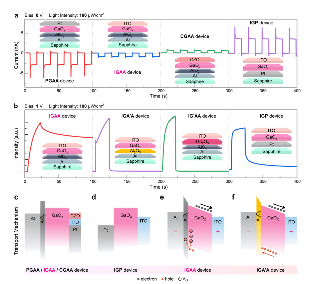
Figure 3 Mechanistic investigation of the dual-mode operation and interfacial physics. (a) Time-dependent photocurrent responses of the PGAA, IGAA, CGAA, and IGP devices under 0 V bias and 254 nm UV illumination, illustrating the influence of interfacial potential barriers on self-powered detection; (b) Normalized I–t characteristics of the IGAA, IGA′A, IG′AA, and IGP devices measured at 1 V bias, highlighting the critical role of interfacial oxygen vacancies in determining the persistent photoconductivity; (c,d) Schematic energy-band diagrams of the PGAA, IGAA, CGAA, and IGP devices under 254 nm UV excitation at 0 V, depicting the carrier separation driven by asymmetric built-in fields; (e,f) Energy-band diagrams of the IGAA and IGA′A devices under 1 V bias, illustrating the hole trapping and recombination suppression mechanism. Note: G′ denotes amorphous Ga₂O₃ prepared in an oxygen-rich atmosphere and A′ denotes directly sputtered Al₂O₃ dielectric interlayer
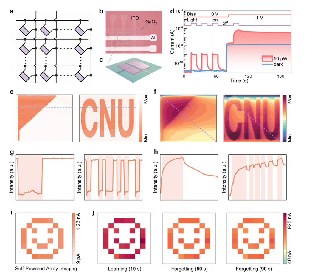
Figure 4 Demonstration of the dual-mode array in single-pixel/array imaging and visual memory. (a) Schematic illustration of the 10 × 10 crossbar array architecture; (b) metallographic microscope image of the fabricated array; (c) schematic illustration of an individual device node within the crossbar. (d) Time-resolved current responses of a representative device pixel. The applied bias switches from 0 V (0–80 s, self-powered photodetection mode) to 1 V (80–200 s, optoelectronic synaptic mode), which verifies a stable and seamless transition between dual working modes of the device. (e) Single-pixel imaging reconstructions of “flag” and “CNU” patterns at 0 V (self-powered mode); (f) Corresponding single-pixel imaging patterns at 1 V (synaptic mode), exhibiting characteristic “tailing” effects due to signal retention. (g) Time-resolved current profile of the 30th row in panel (e) at 0 V. (h) Dynamic current traces along the diagonal pixels in panel (f) at 1 V. (i) High-contrast array imaging of a “smiley face” pattern captured at 0 V. (j) Visual memory of the “smiley face” pattern preserved at 1 V, demonstrating robust image retention capability
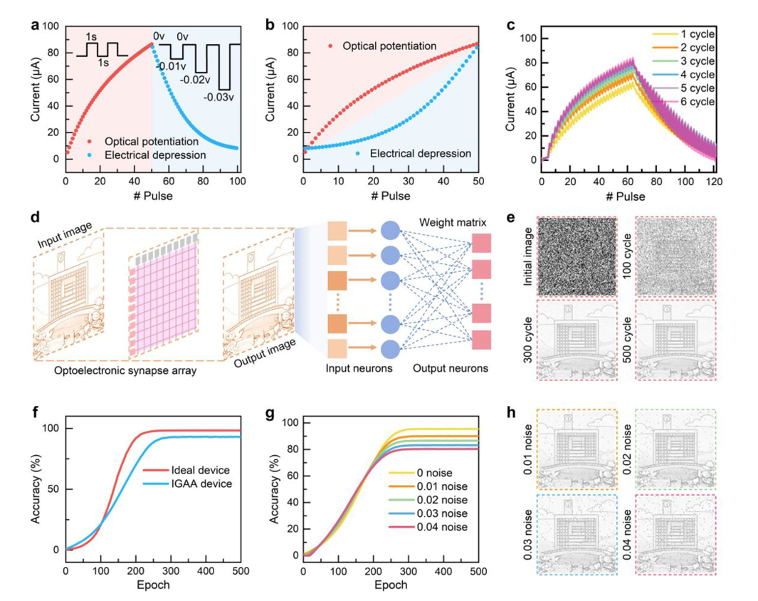
Figure 5 Photo-electric synergistic weight modulation and hardware-driven image recognition of the IGAA-based NVS. (a) Representative long-term potentiation and long-term depression characteristics of a single device under cooperative optical and electrical stimuli. (b) Successive pulse-induced conductance updates demonstrate symmetric and linear weight modulation. (c) Reproducible LTP–LTD cycles highlight the excellent operational stability and endurance of the synaptic device. (d) Schematic illustration of the IGAA-based neuromorphic visual system for intelligent image processing. (e) Evolution of the image reconstruction process, showing the progressive transition from a noisy initial state to a clear target pattern over 500 training epochs. (f) Recognition accuracy as a function of training epochs, comparing the IGAA-based NVS with an idealized software-based model. (g) Evolution of recognition accuracy under various Gaussian noise levels (σ = 0.01–0.04). (h) Final recognition results after 500 epochs at different noise levels, demonstrating the robust noise tolerance of the hardware system
DOI:
doi.org/10.1002/adfm.77328
Instruction
Official Account

Cooperation
Top
