


A photoconductive switch is an optoelectronic device that controls electrical conduction and switching through laser pulses, showing broad application prospects in the field of pulsed power. Its performance highly depends on the breakdown voltage capability, dark-state insulation properties, and photoresponse characteristics of the substrate material.
As a fourth-generation ultra-wide-bandgap semiconductor, gallium oxide (Ga₂O₃) features an ultra-wide bandgap of approximately 4.8 eV and a breakdown electric field strength of up to 8 MV/cm, making it highly suitable for photoconductive switch applications. Targeting this emerging field, Hangzhou Garen Semiconductor Co., Ltd. (hereinafter referred to as “Garen Semiconductor”) has developed and launched customized semi-insulating Ga₂O₃ substrates specifically designed for photoconductive switches, leveraging its proprietary casting-based crystal growth technology.
The newly released substrates provide robust material support for the development of ultra-high-voltage and ultra-fast-response photoconductive devices. The products are currently available with sufficient production capacity and ready stock supply.
Technical Highlights of the Semi-Insulating Substrate Wafer
1. Excellent crystal quality and atomically smooth surface. X-ray diffraction (XRD) rocking curve measurements show that the substrate achieves an ultra-low full width at half maximum (FWHM) of 29 arcsec, indicating high crystalline integrity and low defect density. Atomic force microscopy (AFM) measurements reveal an extremely low surface roughness of only 0.140 nm, reaching atomic-level smoothness. These outstanding substrate characteristics meet the stringent surface-quality requirements for advanced device fabrication and provide a solid foundation for the development of high-performance devices.
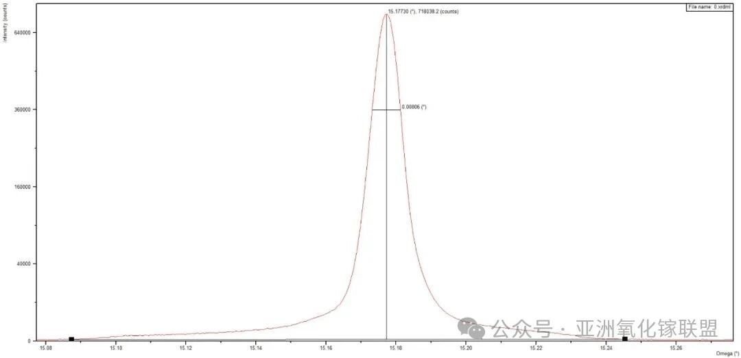
Figure 1. XRD rocking curve measurement results of the semi-insulating substrate developed by Garen Semiconductor
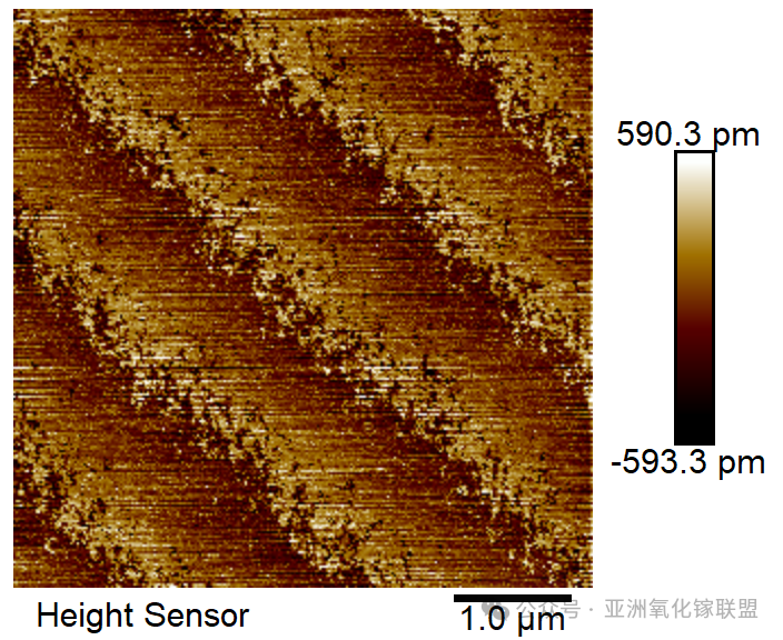
Figure 2. AFM measurement results of the semi-insulating substrate developed by Garen Semiconductor
2. The substrate exhibits excellent resistivity performance and superior switching-off characteristics. With a resistivity exceeding 1 × 10¹¹ Ω·cm, the substrate demonstrates outstanding semi-insulating properties, effectively suppressing dark-state leakage current. This enables devices to withstand high voltages in the off-state while maintaining low leakage levels, providing critical material support for achieving high on/off ratios and fast switching performance.
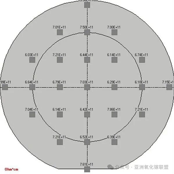
Figure 3. Resistivity measurement results of Garen Semiconductor’s semi-insulating substrate.
3. Device-level validation demonstrates internationally leading performance. Based on semi-insulating substrates provided by Garen Semiconductor, a research team from the Shenzhen Pinghu Laboratory developed Mg-doped vertical photoconductive switches. Experimental measurements demonstrated a breakdown electric field exceeding 220 kV/cm, an on/off switching ratio reaching the 10¹¹ level, a breakdown voltage above 10,000 V, a dynamic on-resistance below 10 Ω, and an off-state switching time shorter than 1 ns. Multiple key performance metrics rank among the leading levels worldwide. The outstanding device performance further validates the high quality and reliability of Garen Semiconductor’s semi-insulating substrates.
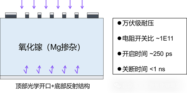
Figure 4. Structure and performance characteristics of the Mg-doped Ga₂O₃ photoconductive switch (Image source: Shenzhen Pinghu Laboratory)
Product Specifications
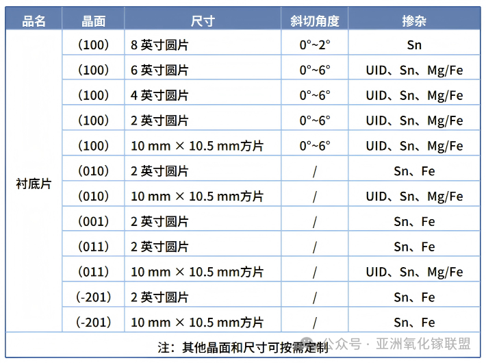
Figure 5. Garen Semiconductor substrate product portfolio.
Key parameters, including doping schemes, substrate sizes, and crystal orientations, can be customized according to specific requirements to meet the needs of devices with different voltage ratings and response speed requirements. For further information on product details, please contact the sales and technical support teams of Garen Semiconductor.
Device performance breakthroughs are fundamentally driven by advances in underlying materials. The launch of Garen Semiconductor’s customized semi-insulating Ga₂O₃ substrates for photoconductive switch applications marks a key strategic step in the field of pulsed power technologies. It provides a stable, controllable, and highly customizable domestic substrate solution for the development of ultra-high-voltage photoconductive devices in China.
The product is now officially available for sale with sufficient production capacity. Garen Semiconductor welcomes partners to collaborate in advancing Ga₂O₃-based photoconductive switches from material innovation to device implementation, and from technological breakthroughs toward industrial maturity.
About Garen Semiconductor
Hangzhou Garen Semiconductor Co., Ltd. is a global provider of gallium oxide materials and equipment solutions, specializing in the R&D and commercialization of ultra-wide-bandgap semiconductor technologies. The company’s core products include 2–8 inch gallium oxide single crystals and substrates (including the world’s first 8-inch products), vertical Bridgman (VB) gallium oxide crystal growth equipment, and 2–8 inch gallium oxide homoepitaxial wafers (including the world’s first 8-inch products). Garen Semiconductor is dedicated to building a fully integrated “equipment–crystal growth–substrate–epitaxy” industrial ecosystem and providing comprehensive solutions for global customers. The company’s achievements in gallium oxide have been widely recognized and featured by leading media outlets, including People’s Daily, Xinhua News Agency, Science and Technology Daily, Sina Finance, China Blue News, and The Paper.
For more information, please visit the official website: http://garen.cc/
Or contact us:
Mr. Jiang
Phone: +86 159 1871 9807
Email: jiangjiwei@garen.cc
Mr. Xia
Phone: +86 190 1127 8792
Email: xianing@garen.cc
Instruction
Official Account

Cooperation
Top
