


Researchers from Nanjing University of Posts and Telecommunications have published an article titled “Influence of Dry Etching and Surface Repair on the Electrical Performance and Reliability of β-Ga₂O₃ Schottky Barrier Diodes” in IEEE Transactions on Electron Devices.
Background
β-Ga₂O₃ is an ultrawide bandgap semiconductor with a bandgap of ~ 4.8–4.9 eV, a critical electric field of 8 MV/cm and a Baliga’s figure of merit superior to SiC and GaN. Large-size native substrates can be fabricated via melt-growth methods, making it an ideal candidate for high-voltage high-efficiency power devices. Schottky barrier diodes (SBDs) feature simple structure and fast switching speed, which are core components of Ga₂O₃ power devices. Trench and field-plate structures for high breakdown voltage all require plasma dry etching. However, ion bombardment induces lattice disorder and massive interfacial defects, raising reverse leakage current and degrading ideality factor. These defects act as degradation precursors and severely reduce long-term device reliability. Previous works only focus on static electrical recovery after etching, lacking quantitative analysis on how etch damage affects device reliability under bias and high temperature. The carrier transport degradation mechanism induced by interfacial defects is also unclear. Tetramethylammonium hydroxide (TMAH) wet treatment can repair etched surfaces, while its improvement on device stress stability has not been fully demonstrated. In this work, three groups of diodes including untreated, dry-etched and etched-with-TMAH-repaired samples are fabricated. The measure-stress-measure (MSM) protocol is adopted to systematically study the regulation of etch damage and TMAH repair on static characteristics, high-temperature and bias reliability, providing experimental guidance for post-etch surface treatment of high-reliability β-Ga₂O₃ power devices.
Abstract
The fabrication of advanced high-voltage β-Ga₂O₃ Schottky barrier diodes (SBDs) frequently relies on plasma-based dry etching techniques; however, the process introduces surface damage and interface states that degrade device performance and may also compromise the long-term reliability. This work presents a comprehensive investigation of dry-etch-induced degradation and the effectiveness of tetramethylammonium hydroxide (TMAH) treatment in repairing the etched surface. Systematic electrical characterization reveals that dry etching broadens the barrier-height distribution and enhances reverse leakage. Conversely, TMAH treatment effectively restores barrier uniformity and suppresses parasitic transport paths. ON-state reliability was evaluated under various stress voltages and temperatures. The etch-treated devices exhibit the most severe performance variation, with turn-on voltage shifts exceeding 23.85% under 7-V stress and 34.56% at 400 K, together with strong leakage current escalation and the emergence of trap-assisted transport after stress. TMAH-treated devices demonstrate greatly improved stability, showing degradation trends comparable to or smaller than those of unetched SBDs. The findings demonstrate that device reliability is more sensitive to interface treatment than static electrical metrics alone suggest and highlight the necessity of post-etch repair for achieving robust Ga₂O₃ power devices.
Highlights
Three contrast groups of β-Ga₂O₃SBDs (untreated, only dry-etched, etched + TMAH repaired) are fabricated without mesa or passivation, realizing pure interface comparison of damage and recovery effect;
AFM, CV, temperature-dependent J-V and PF/SE transport models are combined to quantitatively verify plasma etching generates massive interface states, broadens barrier inhomogeneity and creates shallow traps triggering Poole-Frenkel leakage;
Multi-bias (4 / 5 / 6 / 7 V) and multi-temperature (300 / 350 / 400 K) MSM stress-recovery measurements are carried out to quantify V_on and barrier shift of three device groups;
The degradation amplitude of etched devices is more than twice that of TMAH-repaired samples, and the gap enlarges at high temperature. TMAH passivates both native and etching-induced interfacial defects;
Degradation mechanism is clarified: dry etching introduces shallow traps to capture carriers under stress and raise barrier height continuously; TMAH planarizes surface, reduces D_it and suppresses trap-assisted leakage and parameter drift.
Conclusion
This work systematically elucidates the influence of dry-etch-induced surface damage and TMAH-based repair on the electrical characteristics and reliability of β-Ga₂O₃ Schottky barrier diodes. Dry etching was shown to reduce the Schottky barrier height, broaden the barrier-height inhomogeneity, and enhance reverse leakage through additional transport paths. These interface disorders also act as performance shift precursors, resulting in substantial turn-on voltage shifts and elevated leakage currents under forward-bias and high-temperature stresses. Etch-treated devices consistently exhibited the greatest performance shift, confirming that reliability is highly sensitive to plasma-induced surface defects. In contrast, TMAH treatment effectively restored the Schottky interface, yielding barrier-height and transport characteristics comparable to or better than those of untreated devices. Under electrical and thermal stress, TMAH-treated SBDs demonstrated significantly improved stability and suppressed defect activation, with markedly lower performance degradation. These findings establish a clear framework for optimizing surface treatment strategies aimed at achieving high-performance and high-reliability β-Ga₂O₃ power devices.
Project Support
This work was supported by the National Natural Science Foundation of China under Grant 62304113, in part by the Frontier Technologies Research and Development Program of Jiangsu Province under Grant BF2025078, and in part by the Natural Science Research Start-up Foundation of Recruiting Talents of Nanjing University of Posts and Telecommunications under Grant NY224021.
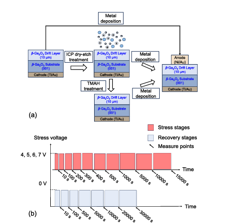
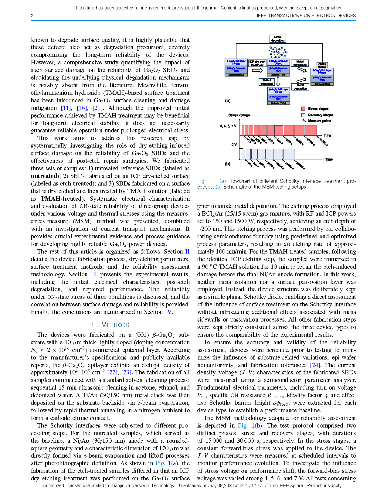
Figure 1 (a) Schematic fabrication flow of three device groups; (b) Schematic timeline of measure-stress-measure (MSM) test
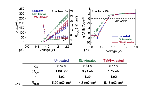
Figure 2 (a) Forward J-V curves and specific on-resistance of three SBDs; (b) Logarithmic forward J-V characteristics; (c) Summary table of key electrical parameters
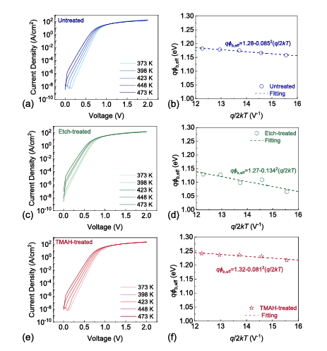
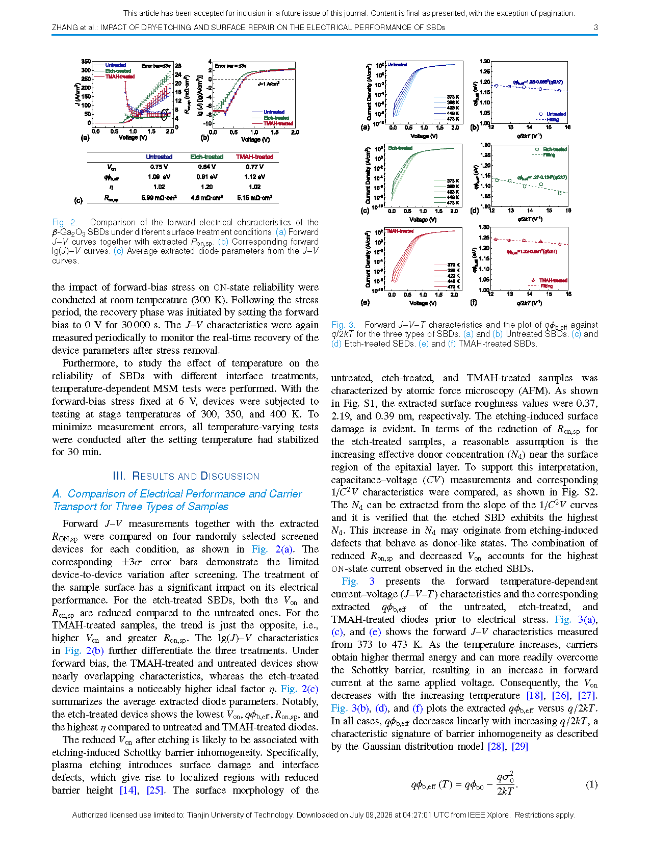
Figure 3 (a)(c)(e) Temperature-dependent forward J-V curves of untreated / etched / TMAH-treated devices; (b)(d)(f) Fitting plots of qφb,eff versus q/2kT
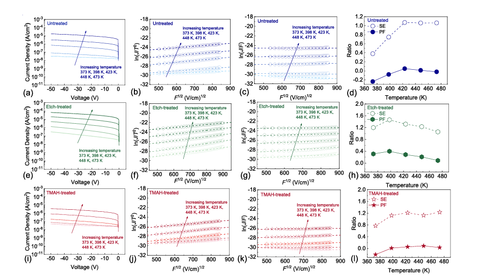
Figure 4 Reverse J-V-T, ln(J/T²)-F¹ᐟ², ln(J/F)-F¹ᐟ² curves and transport ratio Sfit/Scal for three device types
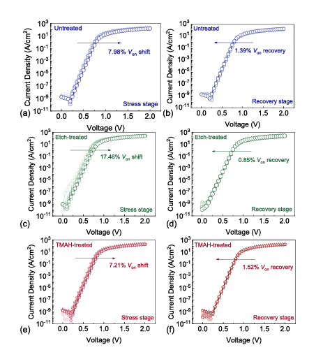
Figure 5 Comparison of J-V evolution of three devices before and after 6 V forward stress (stress stage & recovery stage)
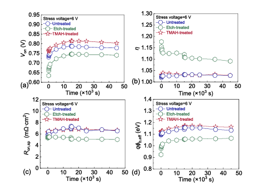
Figure 6 Evolution curves of Von, ideality factor η, Ron,eff and effective barrier height during full stress cycles
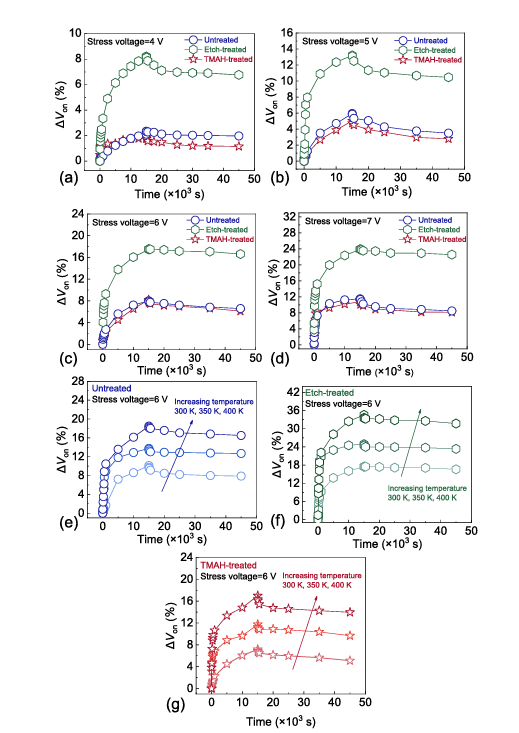
Figure 7 Von shift curves under 4 / 5 / 6 / 7 V stress and 300 / 350 / 400 K thermal stress
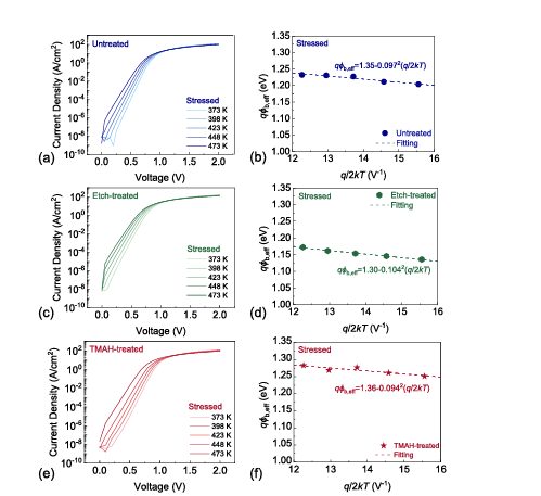
Figure 8 Temperature-dependent forward J-V and barrier fitting plots of three devices after 6 V electrical stress
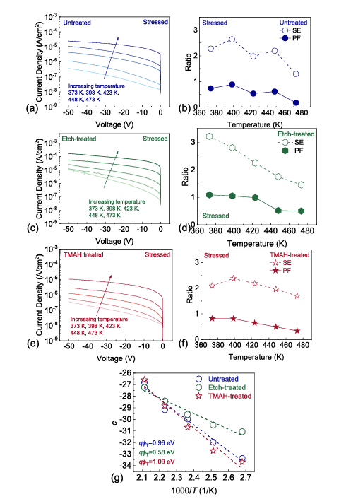
Figure 9 Post-stress reverse J-V-T, transport ratio curves and Arrhenius plot of trap activation energy
DOI:
doi.org/10.1109/TED.2026.3708113
Instruction
Official Account

Cooperation
Top
