


On July 27–29, 2026, the 19th National Conference on MOCVD was held at the Huamao Hotel in Inner Mongolia. Fujia Gallium Technology Co., Ltd. participated in the exhibition with its products, including gallium oxide substrates, epitaxial wafers, and SBD devices. The company was also invited to deliver an academic presentation in Session 4, “Ultra-Wide Bandgap Semiconductors and Emerging Interdisciplinary Frontiers,” showcasing its latest achievements in gallium oxide epitaxy technologies and industrialization.
Chen Duanyang:
Advances in Ga₂O₃ MOCVD Epitaxy Technology and Industrialization
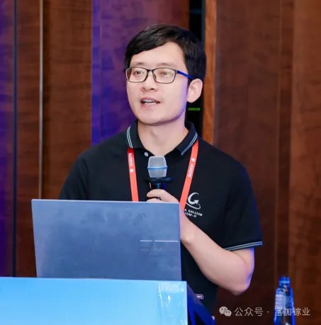
On the morning of July 29, Dr. Chen Duanyang, Deputy General Manager of Fujia Gallium Technology Co., Ltd., delivered an invited presentation titled “Advances in Ga₂O₃ MOCVD Homoepitaxy Technology and Industrialization.”
During the presentation, Fujia Gallium showcased its latest research achievements for the first time: the company has successfully extended its 8-inch Ga₂O₃ epitaxial process to 12-inch wafers, achieving a thickness variation of less than 6% across the 12-inch epitaxial layer, marking a global first.
Dr. Chen highlighted that Fujia Gallium began developing Ga₂O₃ MOCVD epitaxy technology in 2021. By leveraging machine learning-assisted MOCVD process development and conducting a series of process optimizations, the company has achieved mature 6-inch and 8-inch Ga₂O₃ homoepitaxy technologies, with epitaxial wafer performance reaching an internationally leading level.
Building on the superior performance of its epitaxial wafers, Fujia Gallium has collaborated with downstream partners on device development and achieved a series of breakthroughs, enabling the integration of Ga₂O₃ power device development across the entire value chain.
Following its leadership in drafting the first national standard in the Ga₂O₃ field, “Test Method for Dislocation Density Measurement in Single Crystal Polished Wafers of Gallium Oxide by X-ray Topography,” Fujia Gallium is now leading the development of another pioneering national standard on electrical performance testing: “Measurement of Carrier Concentration in Gallium Oxide Epitaxial Layers — Capacitance-Voltage Method.” This represents another milestone in advancing standardization within the Ga₂O₃ industry.
Exhibition Showcase:
Substrates, Epitaxial Wafers, and Devices Displayed Together Across the Entire Value Chain
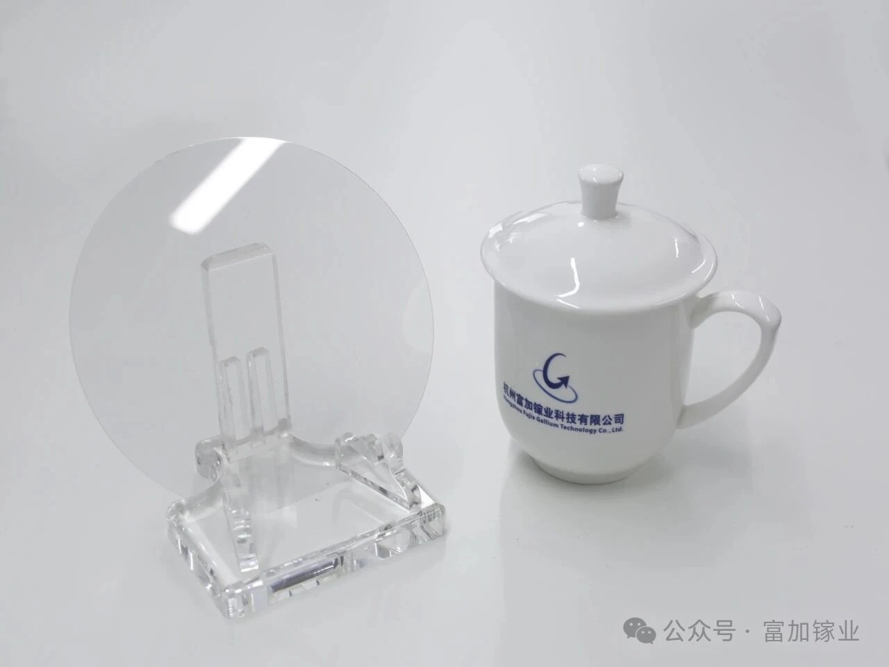
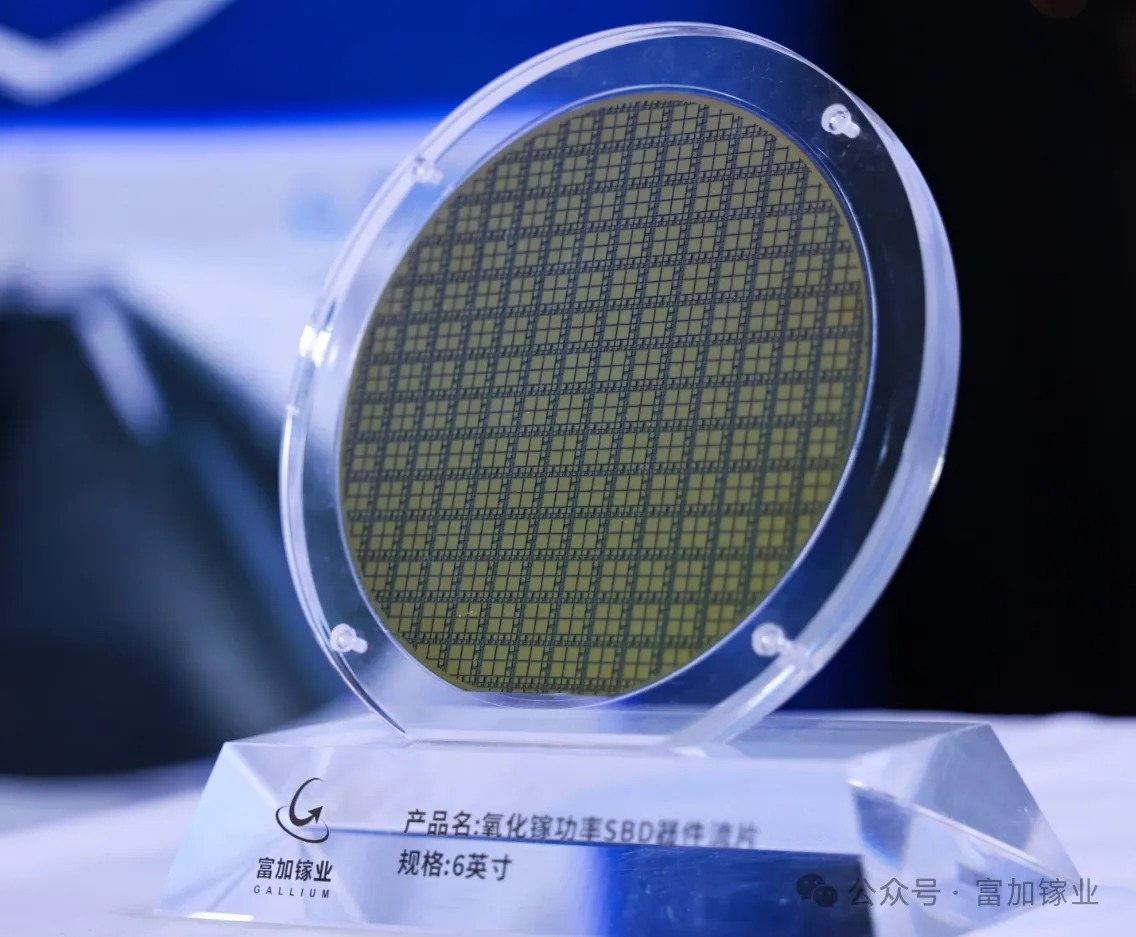
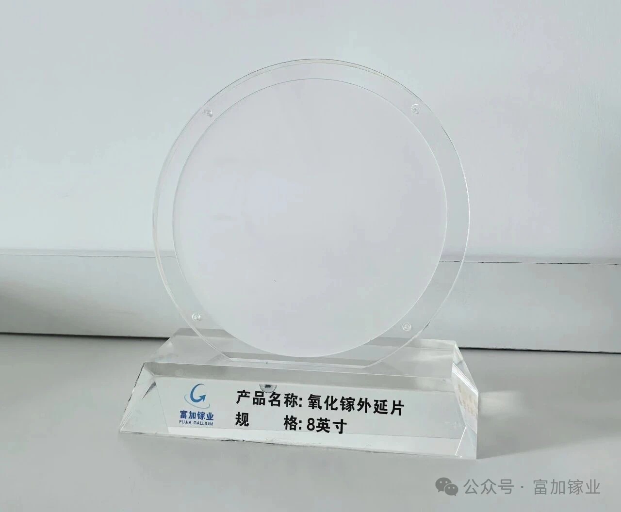
Full Value Chain Product Portfolio
At this year's exhibition, Fujia Gallium showcased three major product categories: 6-inch Ga₂O₃ single-crystal substrates, 8-inch MOCVD Ga₂O₃ homoepitaxial wafers (with electron mobility reaching 209.9 cm²/V·s for 10-μm-thick homoepitaxial layers and surface roughness below 1 nm), and Schottky Barrier Diode (SBD) devices fabricated on 6-inch substrates. Together, these products demonstrated Fujia Gallium's comprehensive industrial capabilities spanning the entire value chain, from materials to devices.
The Fujia Gallium booth attracted strong interest from conference participants. Representatives from leading research institutes and downstream companies engaged in in-depth discussions with the Fujia Gallium team on topics including material supply, device collaboration, and customized solutions.
Industry Exchange:
Advancing the Industrialization of Ga₂O₃
The National MOCVD Conference is one of China's most influential academic platforms for epitaxial materials and semiconductor epitaxy. By participating both as an exhibitor and an invited speaker, Fujia Gallium further strengthened its collaboration with leading domestic research groups and industry partners, laying a solid foundation for accelerating the large-scale application of Ga₂O₃ power devices.
Taking this conference as an opportunity, Fujia Gallium will continue to advance the industrialization of Ga₂O₃ materials. Guided by its mission of " Bringing Better Materials to the World," the company remains committed to contributing to the rapid development of the ultra-wide-bandgap.
About Hangzhou Fujia Gallium
Hangzhou Fujia Gallium Technology Co., Ltd. was established on December 31, 2019. Guided by the vision of “Bringing Better Materials to the World,” the company is dedicated to the industrialization of ultra-wide-bandgap gallium oxide semiconductor materials. Its core products include gallium oxide single-crystal substrates, MOCVD/MBE epitaxial wafers, and crystal growth equipment based on the Vertical Bridgman (VB) and Edge-Defined Film-Fed Growth (EFG) methods. Recognized as a National High-Tech Enterprise, the company has undertaken multiple national and provincial/ministerial-level projects from the Ministry of Science and Technology, the National Development and Reform Commission, and the Ministry of Industry and Information Technology. It has been authorized nearly 70 international and domestic patents, and serves as the initiator and primary drafter of China's national standards in the field of gallium oxide. The company's series of major achievements in promoting gallium oxide industrialization have been featured in special coverages by prominent media outlets, including CCTV, People’s Daily, Xinhua News Agency, China Securities Journal, and The Paper.
Instruction
Official Account

Cooperation
Top
