


Researchers from Guizhou University of Traditional Chinese Medicine, Dalian Minzu University and Guizhou University have published a paper titled “Breaking the Trade-off Between Responsivity and Response Time for Ga₂O₃ Solar-Blind Ultraviolet Photodetectors via Conductive-Bridge Engineering for High-Resolution Dynamic Imaging” in Advanced Functional Materials.
Background
Solar-blind ultraviolet photodetectors only respond to deep ultraviolet light below 280 nm, which are irreplaceable for missile early warning, flame detection, environmental monitoring and deep-space exploration. Conventional β-Ga₂O₃ solar-blind photodetectors face an inherent performance trade-off: deep trap states for high photoconductive gain will prolong carrier lifetime and slow down response speed, while fast carrier transport always sacrifices responsivity. This bottleneck severely restricts practical applications. Existing heterojunction modification methods can only improve either sensitivity or response speed alone, failing to optimize both indicators simultaneously. 2D Nb₂CTₓ MXene owns metallic conductivity to form low-resistance carrier transport channels. Aluminum nanoparticles (Al NPs) produce localized surface plasmon resonance to enhance ultraviolet absorption and build Schottky barriers at the interface for carrier recombination suppression. However, the synergistic conductive bridge regulation effect of these two materials has not been systematically investigated. This work proposes a dual conductive composite strategy of Al NPs/Nb₂CTₓ to construct multi-stage transport channels on β-Ga₂O₃ surfaces, simultaneously breaking the trade-off between responsivity and response speed, and fabricate high-performance solar-blind detectors capable of high-resolution dynamic imaging for static text and moving objects.
Abstract
The inherent trade-off between responsivity and response time fundamentally limits the performance of solar-blind ultraviolet photodetectors (SBUVPDs). Herein, an interfacial conductive-bridge-enhanced charge transport effect is proposed to overcome this limitation. Specifically, the 2D Nb₂CTₓ MXene is introduced to form a charge transport channel at the surface of beta-phase gallium oxide (β-Ga₂O₃). Aluminum (Al) nanoparticles (NPs) are incorporated as an efficient “carrier bridge” at the β-Ga₂O₃/Nb₂CTₓ MXene interface, effectively suppressing carrier accumulation and enhancing charge extraction. Meanwhile, decorating β-Ga₂O₃ with Al NPs enables a synergistic integration of plasmon-enhanced light absorption and improved carrier dynamics via Schottky junction formation. Consequently, the β-Ga₂O₃/Al NPs/Nb₂CTₓ MXene SBUVPDs achieve remarkable performance, featuring a responsivity of 0.64 A/W, a detectivity of 1.01×10¹³ Jones, a low dark current of 8.94×10⁻¹³ A, and a fast response time of 19.1 µs under 250 nm illumination. In addition, the responsivity of the SBUVPDs shows almost no degradation after 10⁴ ON/OFF cycles. Finally, the device demonstrates excellent solar-blind imaging capability for both static letters and realtime moving objects. This work provides a novel and effective design strategy for next-generation high-performance SBUVPDs in imaging and sensing applications.
Highlights
A synergistic dual conductive-bridge modification strategy of Al NPs/Nb₂CTₓ is proposed for the first time, constructing multi-stage carrier transport channels on β-Ga₂O₃ and fundamentally breaking the inherent trade-off between responsivity and response speed;
Nb₂CTₓ MXene film passivates oxygen vacancy defects on β-Ga₂O₃ to drastically reduce dark current. Al NPs introduce localized surface plasmon resonance to boost solar-blind light absorption and build interfacial Schottky barriers for accelerated carrier separation;
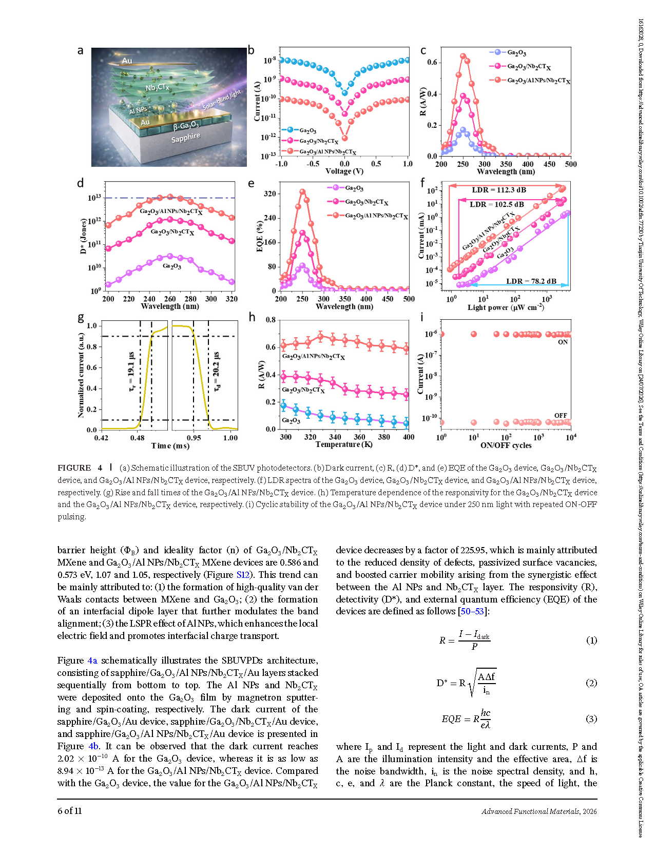
The optimized device achieves high responsivity of 0.64 A/W and ultrahigh detectivity of 1.01×10¹³ Jones under 250 nm illumination, with ultra-fast rise/fall time of 19.1/20.2 µs, realizing high sensitivity and rapid response simultaneously;
The device exhibits a linear dynamic range of 112.3 dB, with negligible performance degradation after 10⁴ ON/OFF cycles, delivering outstanding operational stability and linear photoresponse;
An 8×8 detector array imaging system is constructed, realizing high-resolution real-time solar-blind imaging of static letters and moving targets, which verifies the practical potential of the device for imaging and sensing applications.
Conclusion
In conclusion, a conductive-bridge-enhanced charge transport effect is demonstrated to effectively overcome the trade-off between responsivity and response speed of SBUVPDs. High responsivity and fast response time SBUVPDs were successfully fabricated based on a sapphire/Ga₂O₃/Al NPs/Nb₂CTₓ MXene/Au architecture, achieving a responsivity of 0.64 A/W, a detectivity of 1.01×10¹³ Jones, and rapid rise/fall response times of 19.1/20.2 µs under 250 nm illumination. Relative to pristine β-Ga₂O₃ PDs, synergistic dual-interface engineering endows the β-Ga₂O₃/Al NPs/Nb₂CTₓ MXene heterojunction with suppressed trap states and oxygen vacancies, enhanced electron mobility, and efficient charge separation and transport. Furthermore, the SBUVPDs maintain high stability after 10⁴ continuous ON/OFF cycles. Then, solar-blind imaging of letters and moving objects is successfully demonstrated, exhibiting their promising practical applications.
Project Support
This work is supported by National Natural Science Foundation of China (12404450, 62575047, 62175025), Basic Research Project of Liaoning Provincial Department of Education (LJ212512026009), the Basic Research Program (Natural Science) General Project of Guizhou Province (No.MS[2026]684), Science and Technique Foundation of Dalian (2025RY06), the Doctoral Start-up Grant and Youth Sail Project from Guizhou University of Traditional Chinese Medicine (043250012, QNYFZK[2025]09).
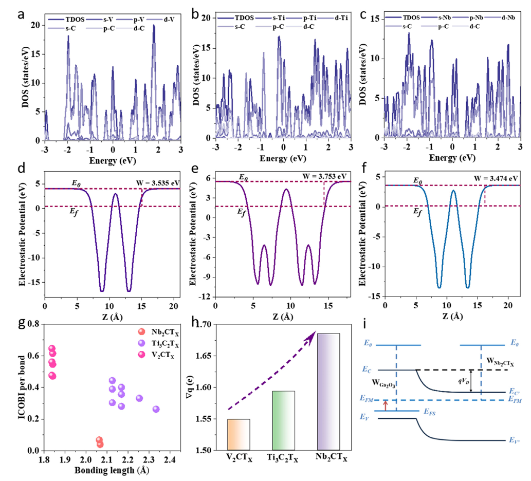
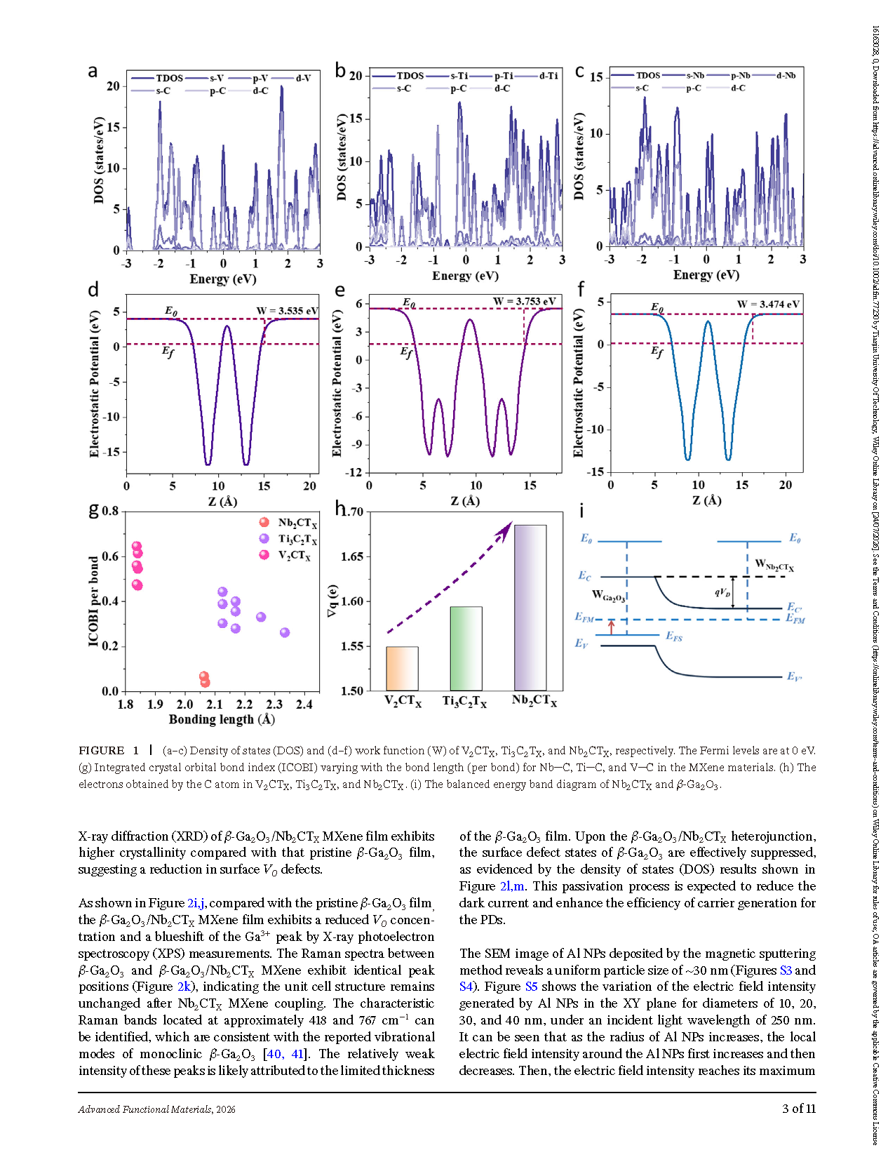
Figure 1 (a–c) Density of states (DOS) and (d–f) work function (W) of V₂CTₓ, Ti₃C₂Tₓ, and Nb₂CTₓ, respectively. (g) Integrated crystal orbital bond index (ICOBI) varying with the bond length (per bond) for Nb-C, Ti-C, and V-C in MXene materials. (h) The electrons obtained by the C atom in V₂CTₓ, Ti₃C₂Tₓ, and Nb₂CTₓ. (i) The balanced energy band diagram of Nb₂CTₓ and β-Ga₂O₃
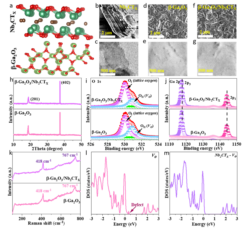
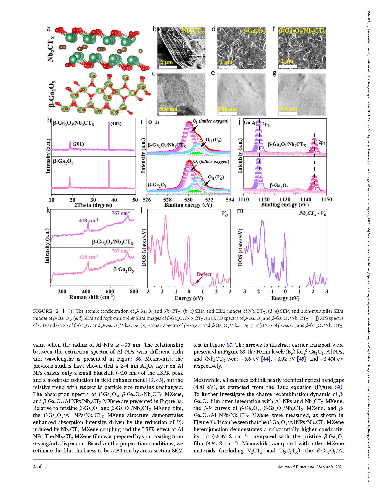
Figure 2 (a) The atomic configuration of β-Ga₂O₃ and Nb₂CTₓ. (b, c) SEM and TEM images of Nb₂CTₓ. (d, e) SEM and high-multiplier SEM images of β-Ga₂O₃. (f, g) SEM and high-multiplier SEM images of β-Ga₂O₃/Nb₂CTₓ. (h) XRD spectra of β-Ga₂O₃ and β-Ga₂O₃/Nb₂CTₓ. (i, j) XPS spectra of O 1s and Ga 2p of β-Ga₂O₃ and β-Ga₂O₃/Nb₂CTₓ. (k) Raman spectra of β-Ga₂O₃ and β-Ga₂O₃/Nb₂CTₓ. (l, m) DOS of β-Ga₂O₃ and β-Ga₂O₃/Nb₂CTₓ
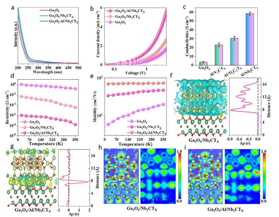
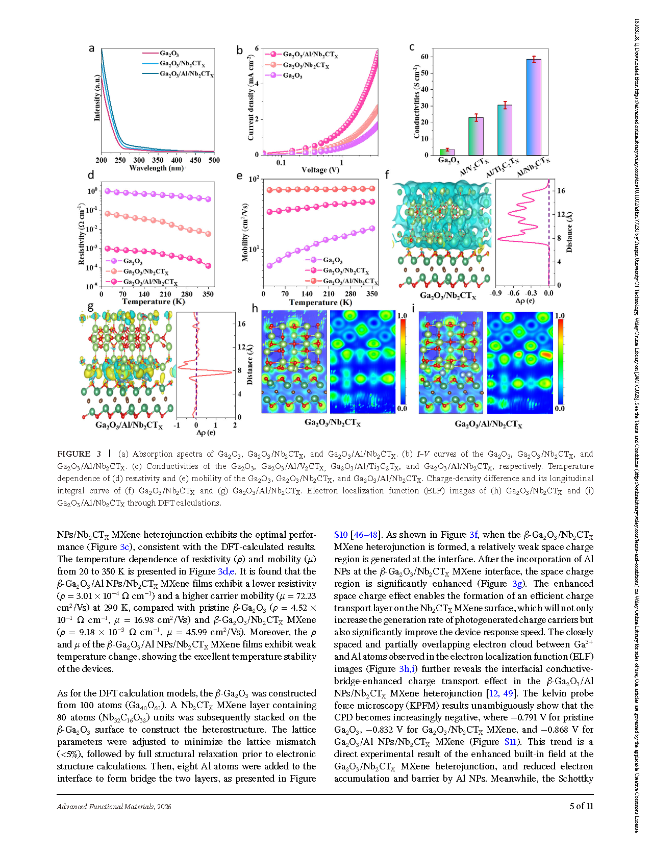
Figure 3 (a) Absorption spectra of Ga₂O₃, Ga₂O₃/Nb₂CTₓ, and Ga₂O₃/Al/Nb₂CTₓ. (b) I-V curves of Ga₂O₃, Ga₂O₃/Nb₂CTₓ, and Ga₂O₃/Al/Nb₂CTₓ. (c) Conductivities of Ga₂O₃, Ga₂O₃/Al/V₂CTₓ, Ga₂O₃/Al/Ti₃C₂Tₓ, and Ga₂O₃/Al/Nb₂CTₓ, respectively. (d) Temperature dependence of resistivity and (e) mobility of the three films. (f) Charge-density difference and its longitudinal integral curve of Ga₂O₃/Nb₂CTₓ; (g) Charge-density difference curve of Ga₂O₃/Al/Nb₂CTₓ. (h, i) Electron localization function (ELF) images of two heterojunctions via DFT calculations
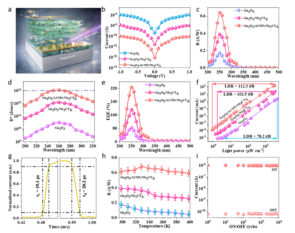
Figure 4 (a) Schematic illustration of the SBUV photodetectors. (b) Dark current, (c) responsivity (R), (d) detectivity (D*), (e) EQE of three devices, respectively. (f) LDR spectra comparison. (g) Rise and fall time normalized current waveform of Ga₂O₃/Al NPs/Nb₂CTₓ device. (h) Temperature dependence of responsivity for two composite devices. (i) Cyclic stability curve under repeated ON/OFF pulsing
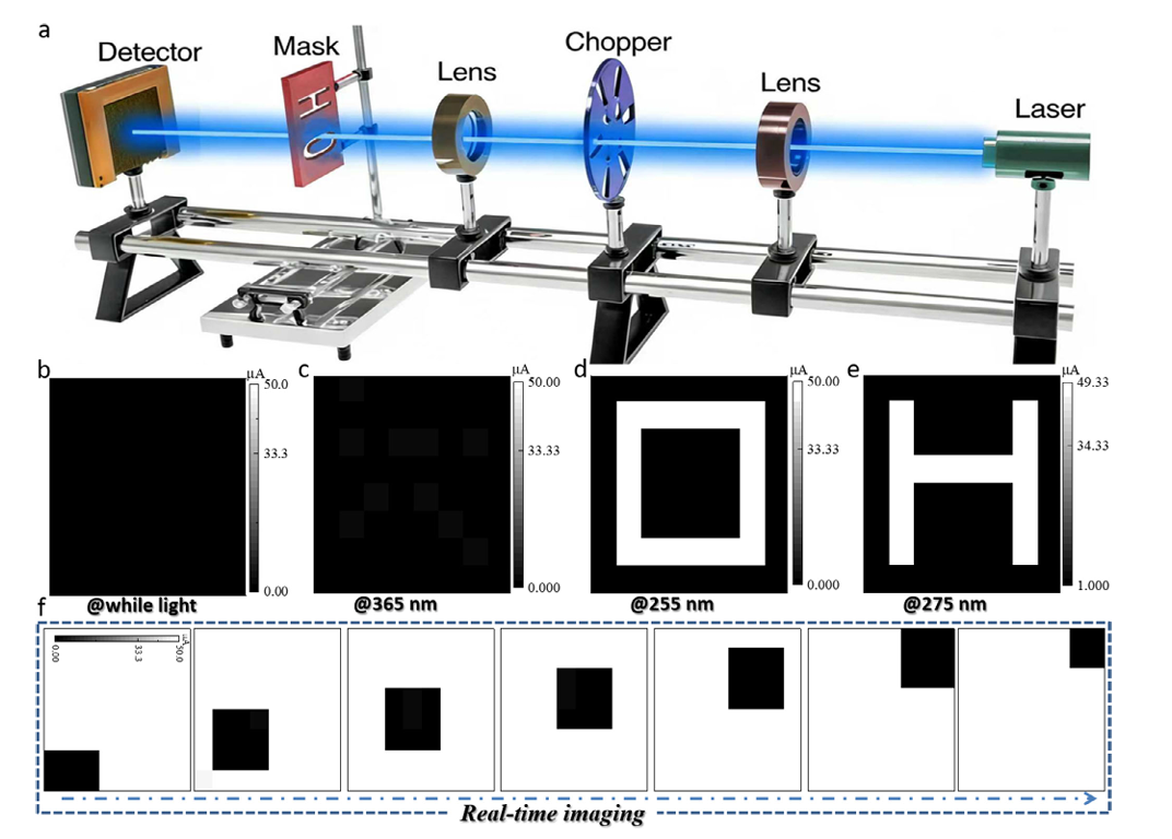
Figure 5 (a) Schematic diagram of the solar-blind imaging system. Imaging current distribution under (b) white light and (c) 365 nm. Imaging output of “O, H” mask under (d) 255 nm and (e) 275 nm. (f) Real-time photocurrent sequence of moving cube target
DOI:
doi.org/10.1002/adfm.77230
Instruction
Official Account

Cooperation
Top
