


Researchers from Wuhan University of Technology, Inner Mongolia University of Technology, Shandong Jingsheng Electronic Technology Co., Ltd, Fuzhou University and Universitas Airlangga (Indonesia) have published a paper titled "Recent Advances in the Mist Chemical Vapor Deposition of Ga₂O₃ Thin Films" in Crystal Growth & Design.
Background
Ga₂O₃, an ultra-wide bandgap semiconductor with bandgap of 4.7–5.6 eV and an ultrahigh theoretical breakdown field up to 8 MV/cm, plays an irreplaceable role in solar-blind ultraviolet photodetectors and high-voltage power devices. Conventional epitaxy technologies including MOCVD, MBE and HVPE require vacuum chambers, leading to high equipment cost and limited large-scale mass production capacity. Mist chemical vapor deposition (mist CVD) operates under atmospheric pressure without vacuum environment, featuring low cost of apparatus and precursors as well as wide tunable solution chemistry, which serves as a promising route for low-cost scalable growth of various Ga₂O₃ polymorphs. Ga₂O₃ has five polymorphs including α, β, γ, δ, ε/κ with distinct electronic and optical anisotropic properties. However, systematic reviews focusing on precise phase control, interfacial buffer layer suppression, elimination of in-plane rotational domains and regulation of impurities/vacancies in mist CVD systems are still absent. This work comprehensively sorts out reactor configurations and growth thermodynamics/kinetics of mist CVD, summarizes research progress covering phase engineering, crystallinity & surface morphology optimization, defect/impurity management, large-area epitaxy and device applications, and analyzes industrial bottlenecks, providing complete theoretical and technical references for low-cost mass fabrication of Ga₂O₃ devices.
Abstract
Gallium oxide (Ga₂O₃), as an emerging ultrawide bandgap semiconductor with high breakdown voltage, excellent thermal and chemical stability, has shown great potential for applications in high-voltage power devices and deep ultraviolet optoelectronic detection. To realize its practical applications, low-cost and large-scale manufacturing techniques are urgently needed. In this context, mist chemical vapor deposition (mist CVD) has emerged as an important candidate for Ga₂O₃ epitaxy, benefiting from its atmospheric-pressure, nonvacuum operation, low equipment and precursor costs, wide process window, and tunable solution chemistry. Hence, this review summarizes the configuration and deposition mechanism of mist CVD. It then systematically reviews recent research progress on the controlled epitaxy of Ga₂O₃, covering phase engineering, regulation of crystallinity and surface morphology, suppression of impurities and defects, interfacial buffer layer control, elimination of in-plane rotational domains, large-area rapid epitaxy, and corresponding device applications. The challenges and prospects of wafer-scale uniform heteroepitaxy and industrial integration are also discussed. This review systematically deconstructs existing technical bottlenecks and provides transformative insights into controllable synthesis of high-quality Ga₂O₃ epitaxial films, offering a clear roadmap toward next-generation ultra-wide bandgap semiconductor power and optoelectronic hardware based on mist CVD.
Highlights
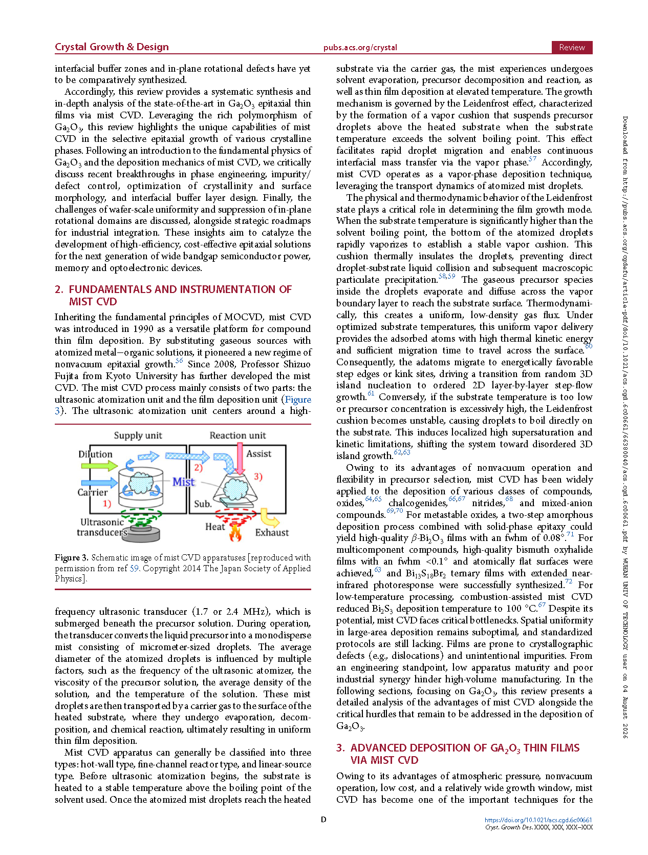
For the first time, this paper fully reviews the full-process thermodynamics and kinetics of mist CVD growth, compares advantages and disadvantages of three reactor types (vertical hot-wall, fine-channel, linear-source), and systematically illustrates the core Leidenfrost droplet growth mechanism;
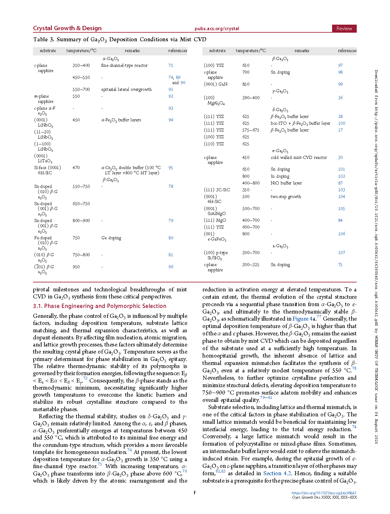
It comprehensively summarizes controllable growth strategies of five Ga₂O₃ polymorphs (α, β, γ, δ, ε/κ) in mist CVD systems, and clarifies four core phase-control variables including temperature, substrate, doping and precursor;
It categorizes three process routes to eliminate in-plane rotational domains including homologous/heterologous buffer layers, vicinal miscut substrates and element doping, and provides feasible approaches to obtain single-domain Ga₂O₃ thin films;
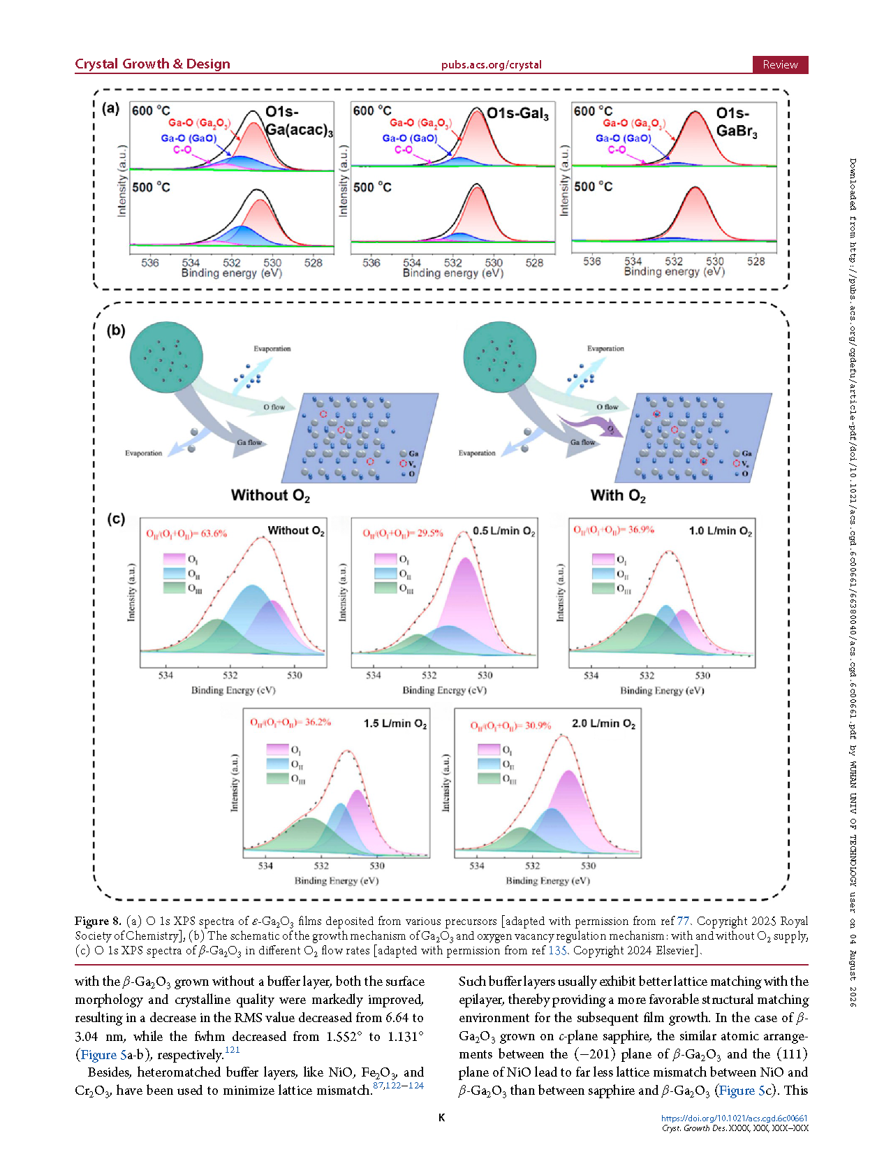
It systematically elaborates formation mechanism and elimination methods of intrinsic oxygen vacancies and extrinsic carbon impurities, and fully compares impurity control performance of halide and acetylacetonate precursors;
It summarizes optimization strategies for wafer-scale uniform epitaxy, sorts out performance merits and existing limitations of mist CVD-fabricated solar-blind photodetectors, Schottky power diodes and neuromorphic ferroelectric devices, and points out industrial optimization directions.
Conclusion
In summary, mist CVD has emerged as a highly promising technique for the epitaxial growth of Ga₂O₃ thin films. Operating under atmospheric pressure without vacuum systems, it offers outstanding cost-efficiency, precursor flexibility, and scalability for industrial wafer production. Over recent years, significant progress has been made in phase-selective epitaxy of α, β, γ, δ, ε / κ polymorphs, improvement of crystalline quality and surface morphology, suppression of carbon impurities and oxygen vacancies, regulation of interfacial buffer layers and mitigation of rotational domains, as well as preliminary achievements in large-area epitaxy. These advances position mist CVD as a core candidate technology for industrial preparation of Ga₂O₃ films and provide strong support for its applications in power devices and deep-ultraviolet photodetectors. To transition mist CVD from laboratory-scale research to commercial semiconductor platforms, three core challenges must be addressed: complete elimination of carbon residue and stable controllable donor activation, realization of single-domain epitaxy on mismatched substrates via advanced substrate and buffer engineering, and development of large-size showerhead reactors for 4–6 inch wafers with uniform thickness and composition. Combined with fluid dynamic simulation and machine learning optimization, mist CVD will unlock the full potential of low-cost Ga₂O₃ electronics in high-power grids and solar-blind detection systems.
Project Support
This work was supported by the National Natural Science Foundation of China (No. 52402200 and 52272161), Hubei Provincial Science and Technology Plan (No. 2025CSA020), and the Chaozhou City Ceramics Industry Talent Revitalization Plan Project (GXYJ001), 2024 Inner Mongolia University of Technology Strategic Priority Research Program - Mechanical Issues in New Energy Equipment and Operation (DC2400003362).
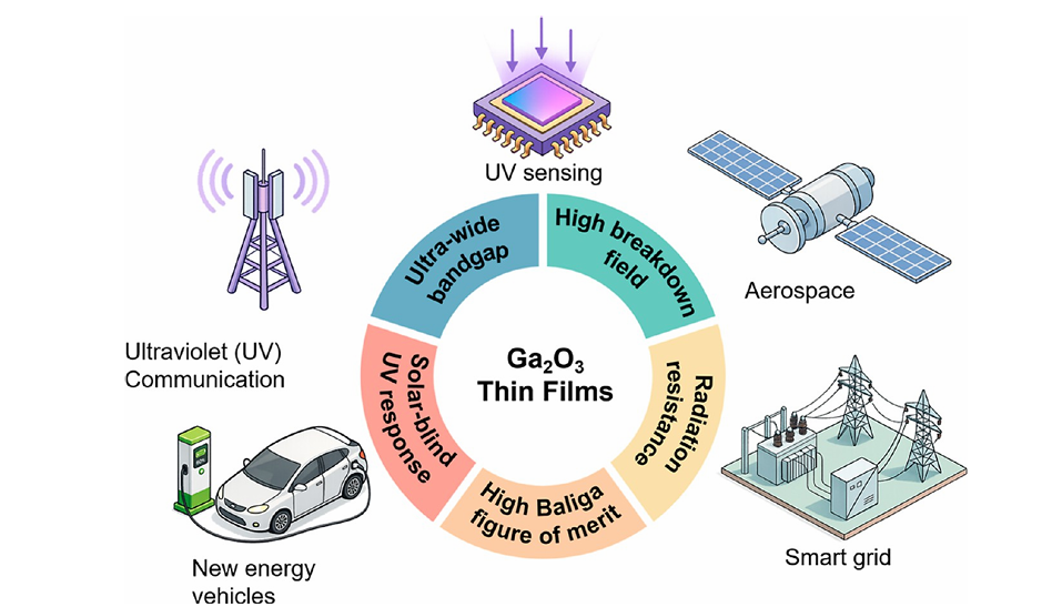
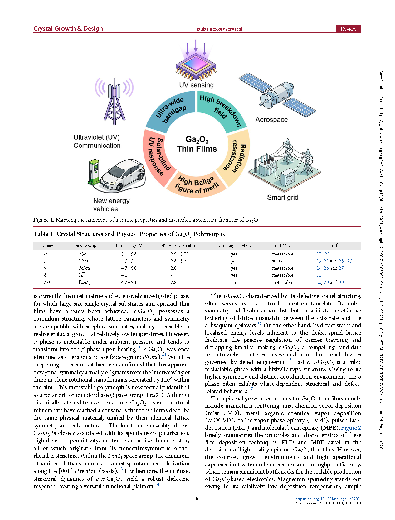
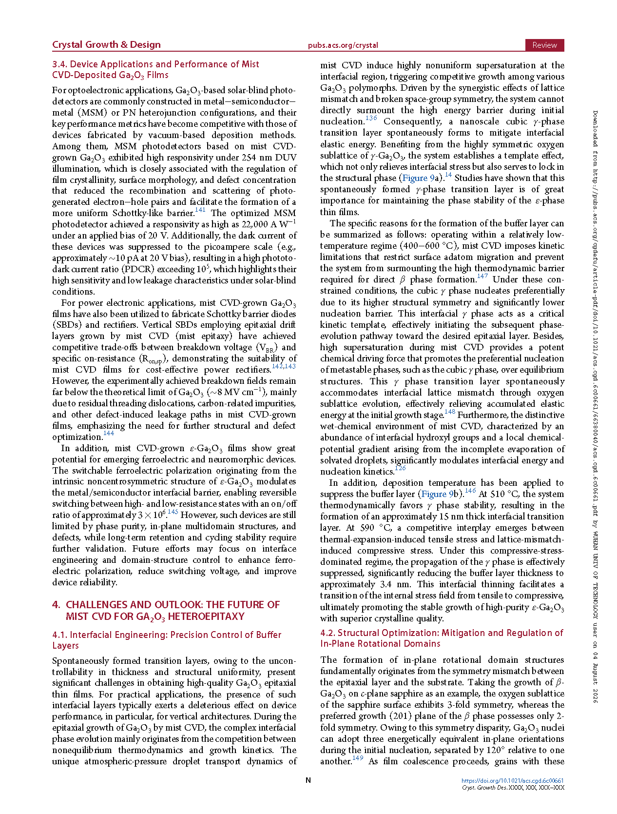
Figure 1. Mapping the landscape of intrinsic properties and diversified application frontiers of Ga₂O₃
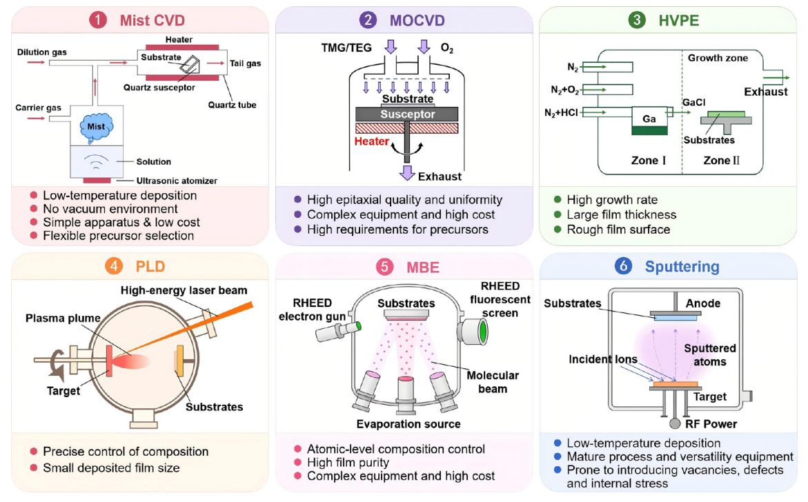
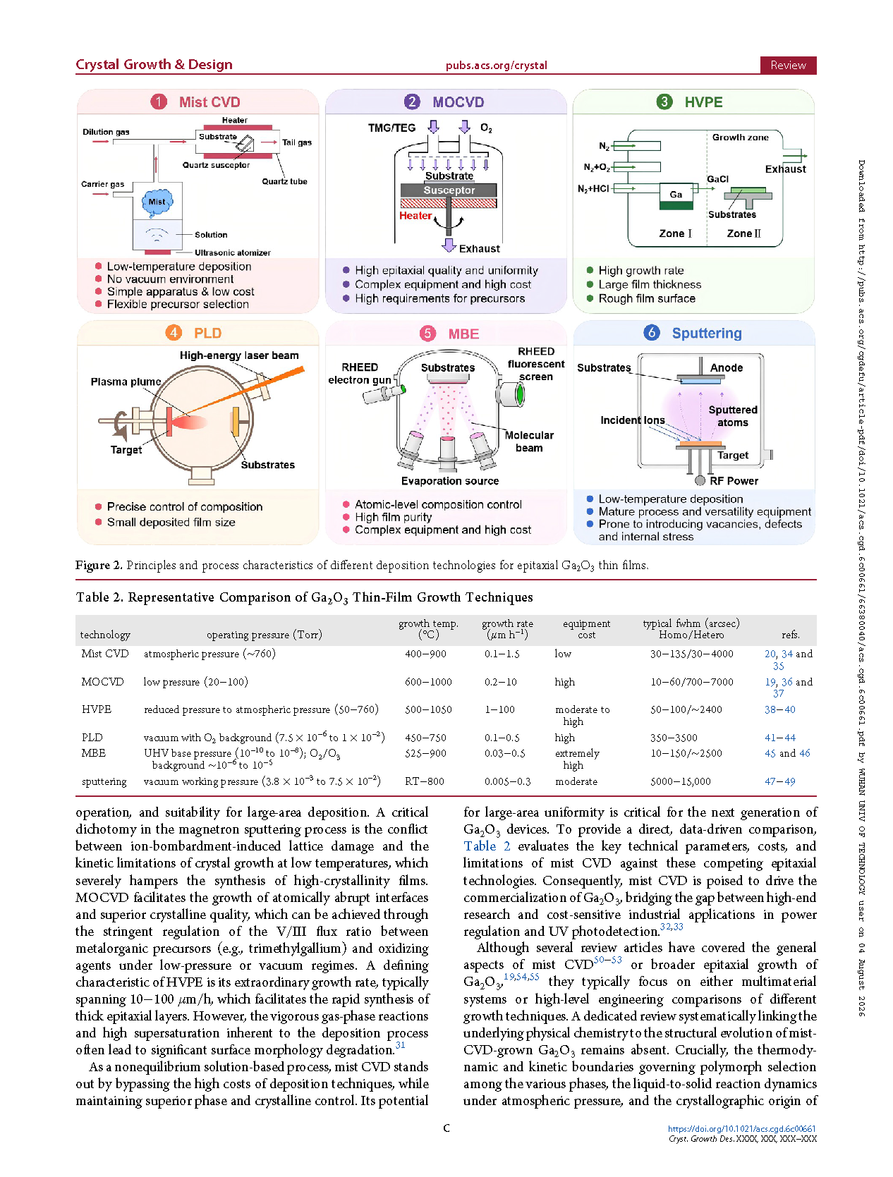
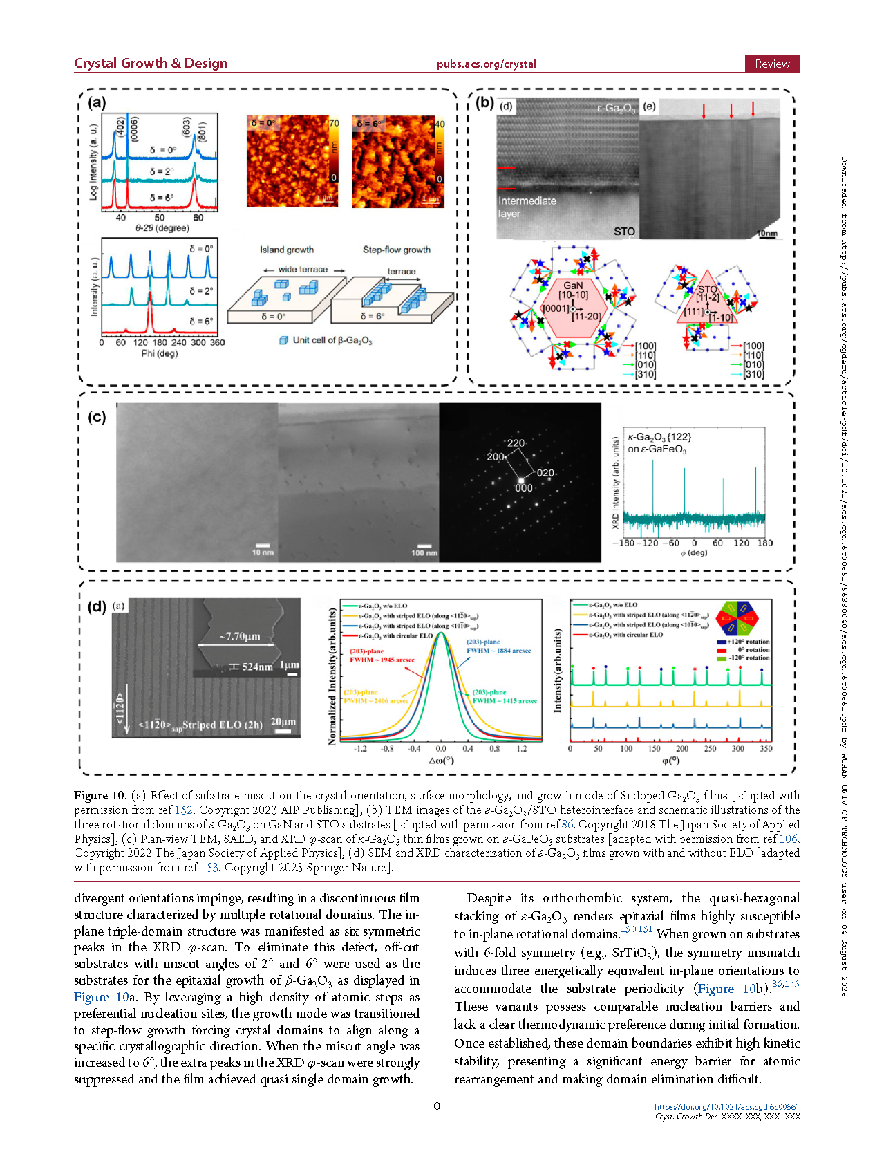
Figure 2. Principles and process characteristics of different deposition technologies for epitaxial Ga₂O₃ thin films
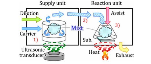
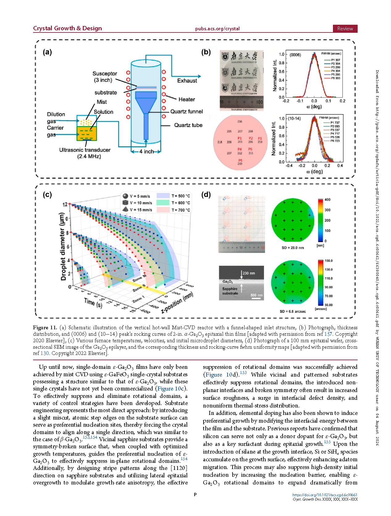
Figure 3. Schematic image of mist CVD apparatuses
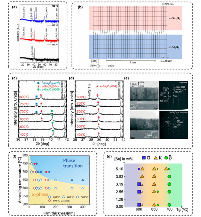
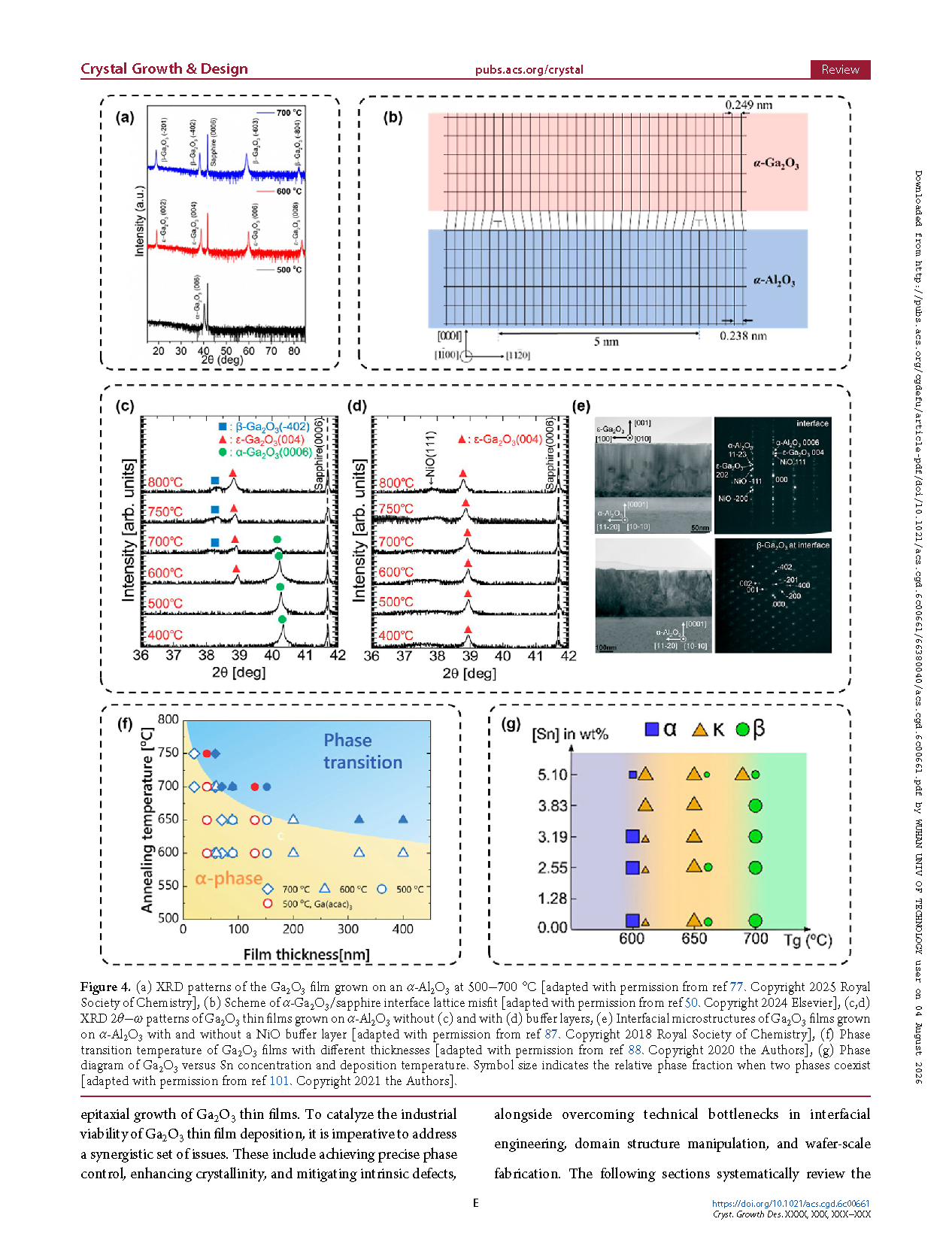
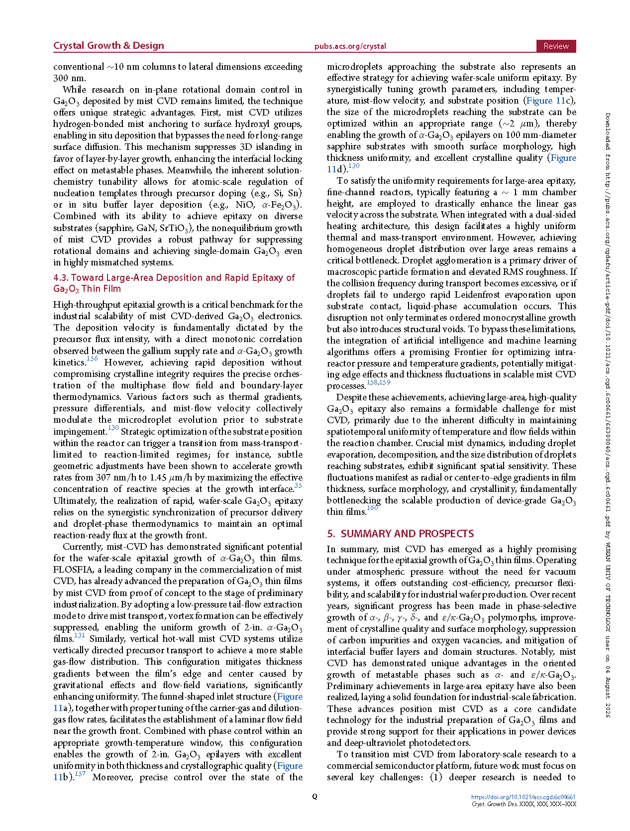
Figure 4. (a) XRD patterns of the Ga₂O₃ film grown on an α-Al₂O₃ at 500−700 °C, (b) Scheme of α-Ga₂O₃ /sapphire interface lattice misfit, (c,d) XRD 2θ−ω patterns of Ga₂O₃ thin films grown on α-Al₂O₃ without and with buffer layers, (e) Interfacial microstructures of Ga₂O₃ films grown on α-Al₂O₃ with and without a NiO buffer layer, (f) Phase transition temperature of Ga₂O₃ films with different thicknesses, (g) Phase diagram of Ga₂O₃ versus Sn concentration and deposition temperature. Symbol size indicates the relative phase fraction when two phases coexist
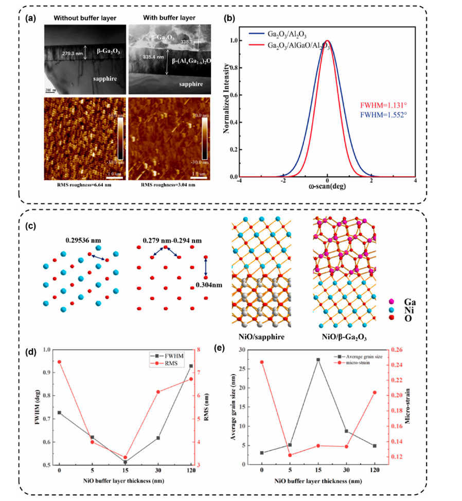
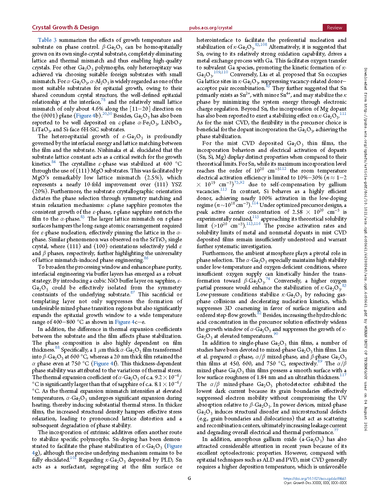
Figure 5. (a) Cross-sectional TEM and surface AFM images, (b) XRD rocking curves of β-Ga₂O₃ films grown with and without β-(AlₓGa₁₋ₓ)₂O₃ interlayer, (c) Oxygen-atom arrangements of NiO and β-Ga₂O₃, and schematic epitaxial relationships of NiO/sapphire and NiO/β-Ga₂O₃, (d) fwhm and RMS of β-Ga₂O₃ with different thickness buffer-layer, (e) Average grain size and microstrain of β-Ga₂O₃ with different thickness buffer-layer
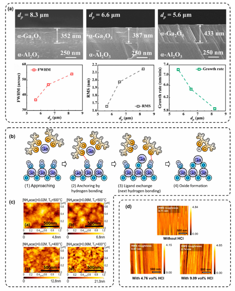
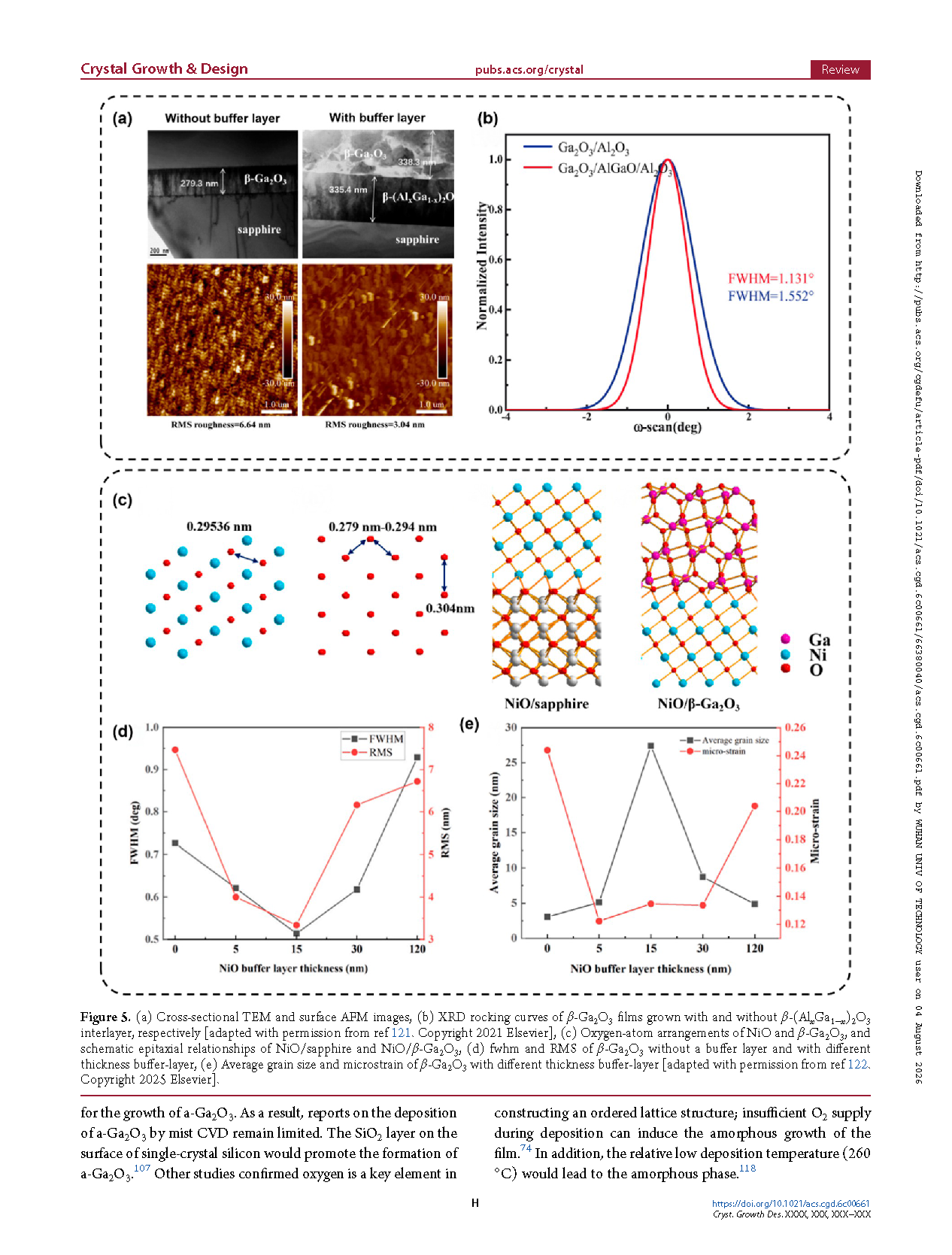
Figure 6. (a) Effect of droplet size (5.6, 6.6, and 8.3 μm) on the thickness, fwhm of (0006) peak, surface roughness, and growth rate of α-Ga₂O₃ thin films, (b) Proposed growth mechanism of α-Ga₂O₃ in mist CVD, (c) AFM images of α-Ga₂O₃ films grown by typical conditions, (d) AFM images of homoepitaxial β-Ga₂O₃ films grown at different HCl concentrations
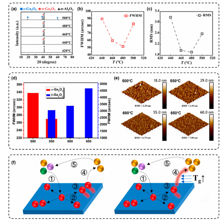
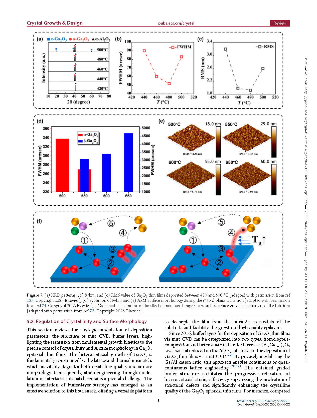
Figure 7. (a) XRD patterns, (b) fwhm, and (c) RMS value of Ga₂O₃ thin films deposited between 420 and 500 °C, (d) evolution of fwhm and (e) AFM surface morphology during the α-to-β phase transition, (f) Schematic illustration of the effect of increased temperature on the surface growth mechanism of the thin film
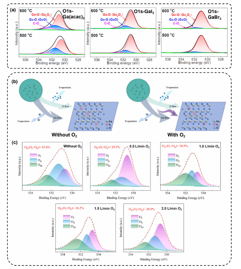
Figure 8. (a) O 1s XPS spectra of ε-Ga₂O₃ films deposited from various precursors, (b) The schematic of the growth mechanism of Ga₂O₃ and oxygen vacancy regulation mechanism: with and without O₂ supply, (c) O 1s XPS spectra of β-Ga₂O₃ in different O₂ flow rates
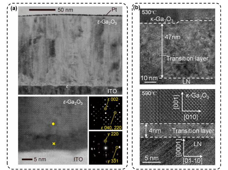
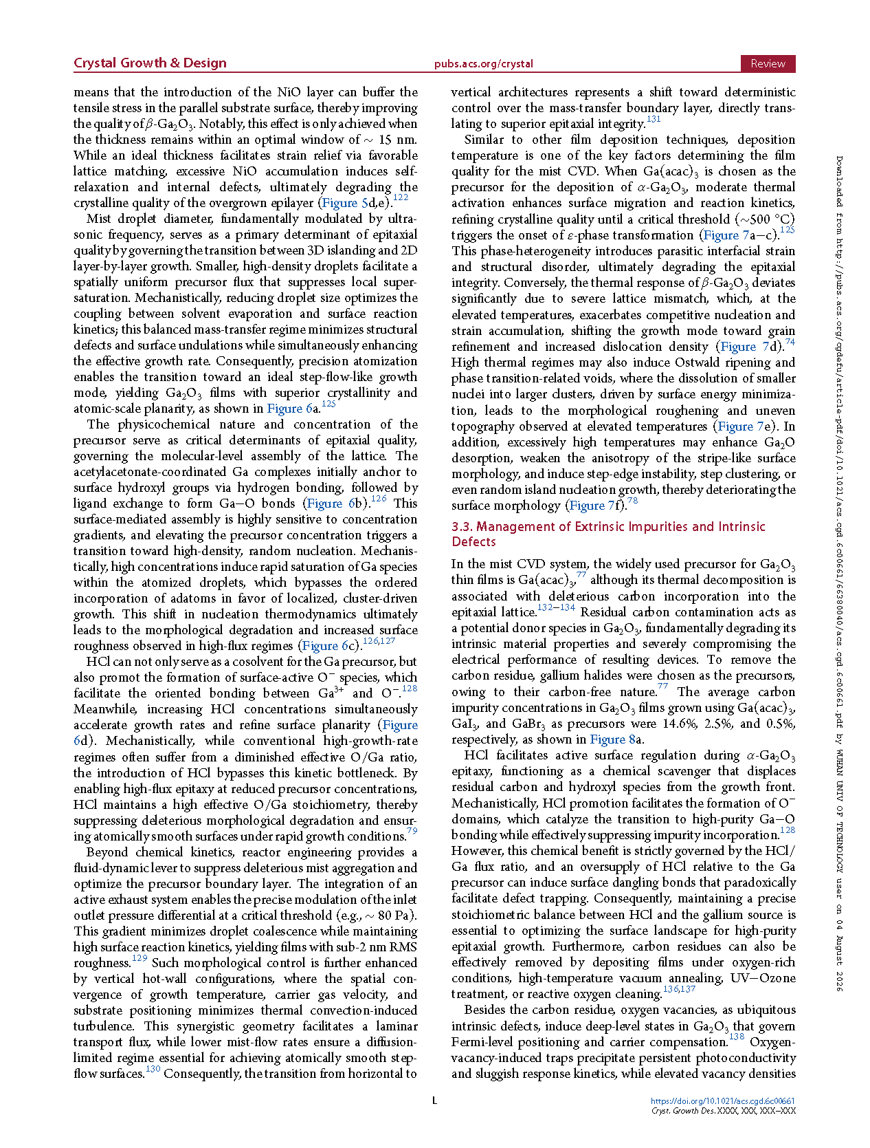
Figure 9. (a) Interfacial microstructure of ε-Ga₂O₃ epitaxial thin film grown on ITO/YSZ: Top: bright-field TEM image near the film/substrate interface. Bottom left: STEM-HAADF image of the interfacial region. Bottom right: SAED patterns taken from the circle-marked and cross-marked regions in the STEM-HAADF image, indexed to ε-Ga₂O₃ and γ-Ga₂O₃, respectively , (b) Cross-sectional HRTEM images of κ-Ga₂O₃ films grown at 530 °C and 590 °C
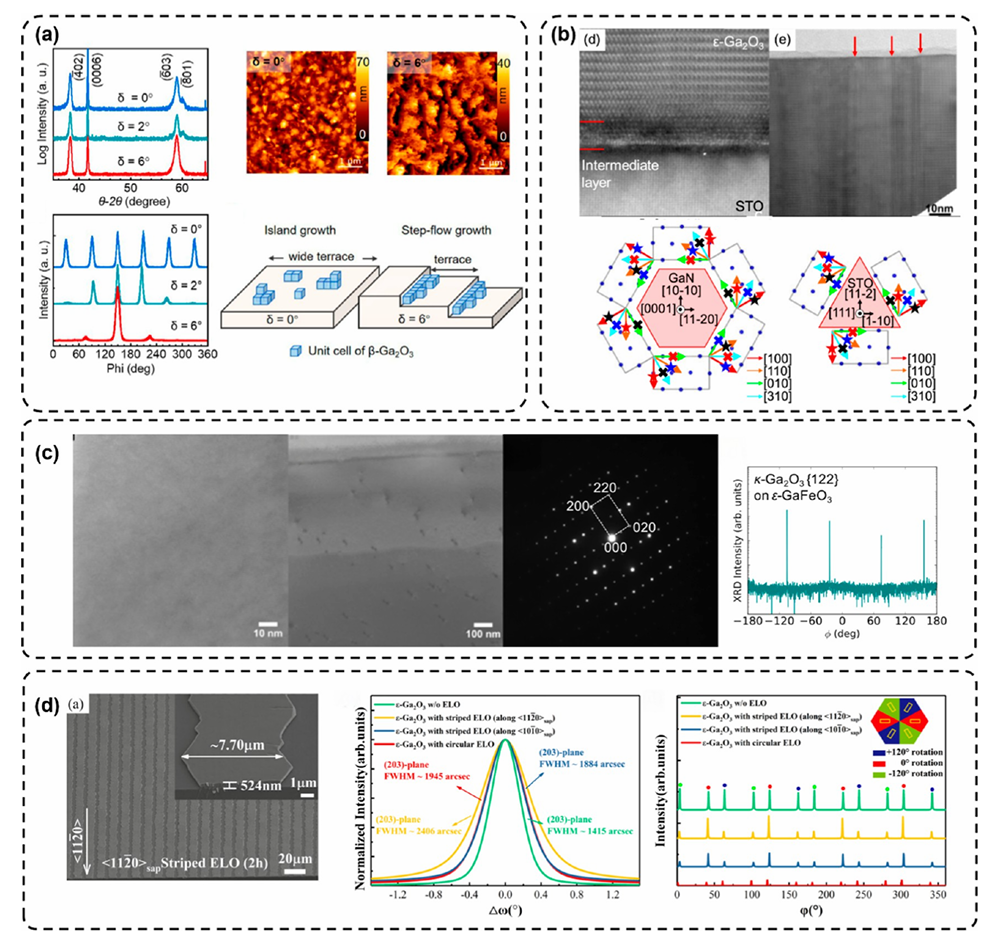
Figure 10. (a) Effect of substrate miscut on the crystal orientation, surface morphology, and growth mode of Si-doped Ga₂O₃ films, (b) TEM images of the ε-Ga₂O₃ / STO heterointerface and schematic illustrations of the three rotational domains of ε-Ga₂O₃ on GaN and STO substrates, (c) Plan-view TEM, SAED, and XRD φ-scan of κ-Ga₂O₃ thin films grown on ε-GaFeO₃ substrates , (d) SEM and XRD characterization of ε-Ga₂O₃ films grown with and without ELO
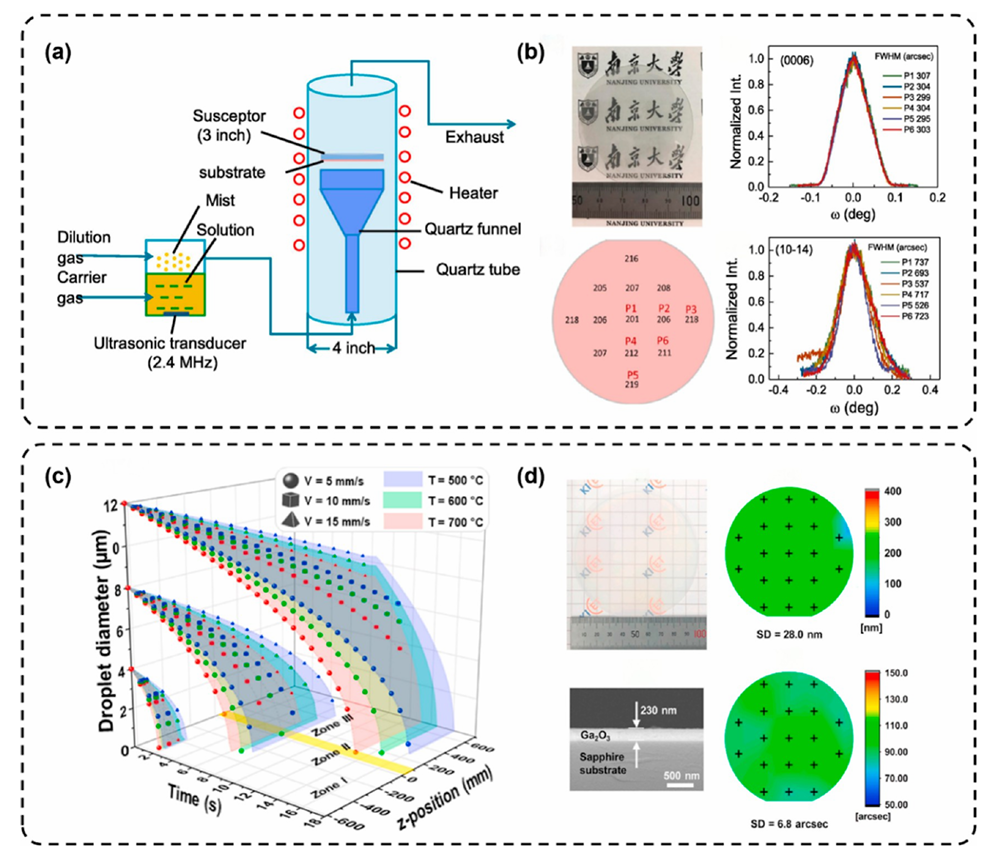
Figure 11. (a) Schematic illustration of the vertical hot-wall Mist-CVD reactor with a funnel-shaped inlet structure, (b) Photograph, thickness distribution, and (0006) and (10−14) peak’s rocking curves of 2-in. α-Ga₂O₃ epitaxial thin films, (c) Various furnace temperatures, velocities, and initial microdroplet diameters, (d) Photograph of a 100 mm epitaxial wafer, crosssectional SEM image of the Ga₂O₃ epilayer, and the corresponding thickness and rocking-curve fwhm uniformity maps
DOI:
doi.org/10.1021/acs.cgd.6c00661
Instruction
Official Account

Cooperation
Top
