


Researchers from National Yang Ming Chiao Tung University and Leibniz-Institut für Kristallzüchtung have published a paper titled "2026 Roadmap for Ultrawide Bandgap β-Ga₂O₃ Semiconductors: From Melt-Grown Materials to High-Voltage Power Devices" in IEEE Electron Devices Magazine.
Background
Global electrification creates rising demands for power electronics. Although SiC and GaN are mature commercial wide-bandgap semiconductors, they still have limitations for ultra-high-voltage applications. As an ultrawide-bandgap semiconductor, β-Ga₂O₃ exhibits a bandgap of 4.5-4.9 eV and a predicted critical electric field of ~8 MV/cm. Uniquely for UWBG materials, scalable native substrates can be manufactured via melt-grown techniques such as Czochralski and EFG. Since the first β-Ga₂O₃ single-crystal transistor was demonstrated in 2012, this field has advanced rapidly. Critical bottlenecks remain: the absence of practical p-type doping, low anisotropic thermal conductivity, high defect density in commercial wafers, and the lack of standardized reliability qualification protocols. This paper reviews bulk crystal growth, epitaxial technologies, various power-device architectures, analyzes material-device-system coupling constraints, and presents near-, medium- and long-term technical roadmaps to support ultra-high-voltage applications such as high-voltage direct-current transmission and pulsed-power systems.
Abstract
The global transition toward electrification demands power electronics beyond the practical limits of silicon. SiC and GaN partially address this challenge but remain constrained in ultrahigh-voltage (ultra-HV) applications by their modest bandgaps (3.3–3.4 eV), medium critical electric fields (3.0–3.3 MV/cm), and costly substrate technologies. β-Ga₂O₃, an ultrawide-bandgap (UWBG) semiconductor, offers a bandgap of 4.5–4.9 eV, a predicted critical electric field approaching 8 MV/cm, and—uniquely among UWBG semiconductors—scalable melt-grown native substrates enabled by Czochralski (Cz) and edge-defined film-fed growth (EFG) techniques. The demonstration of the first single-crystal β-Ga₂O₃ transistor in 2012 initiated rapid progress toward multi-kilovolt (multi-kV) device technologies. Rather than emphasizing record-performance benchmarking alone, this review focuses on design-relevant insights and the material–device–system couplings that define the practical roadmap for β-Ga₂O₃ ultra-HV power electronics.
Highlights
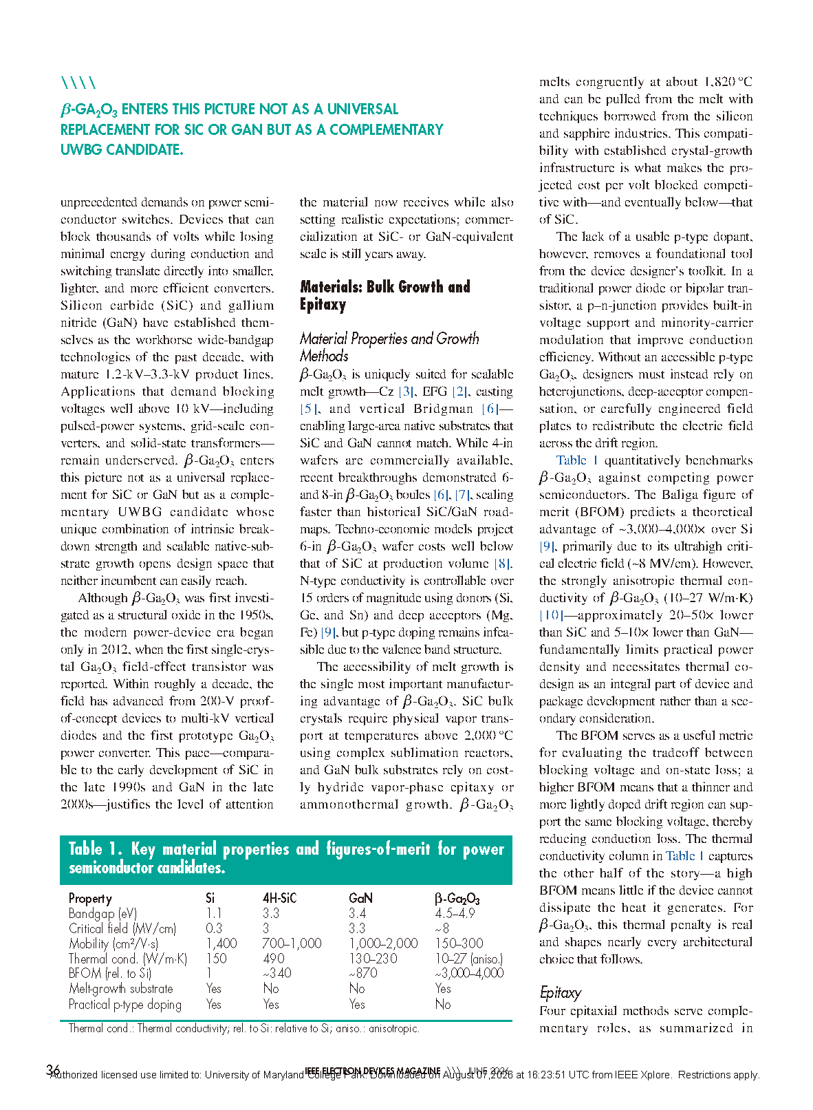
Key intrinsic parameters of β-Ga₂O₃, SiC, GaN and Si are systematically compared. The unique merit of scalable melt-grown native substrates for β-Ga₂O₃ is highlighted, meanwhile two major drawbacks including low thermal conductivity and the lack of practical p-type doping are objectively summarized;
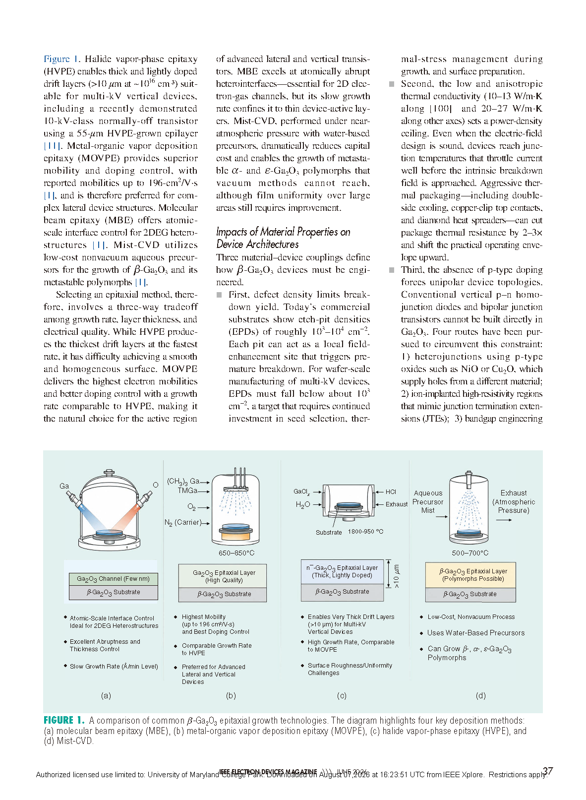
Four mainstream β-Ga₂O₃ epitaxy technologies including HVPE, MOVPE, MBE and Mist-CVD are fully compared, clarifying the trade-offs among growth rate, layer thickness and electrical quality;
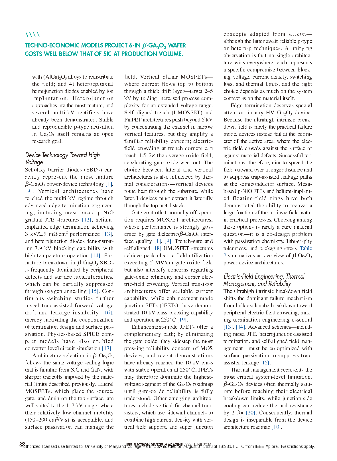
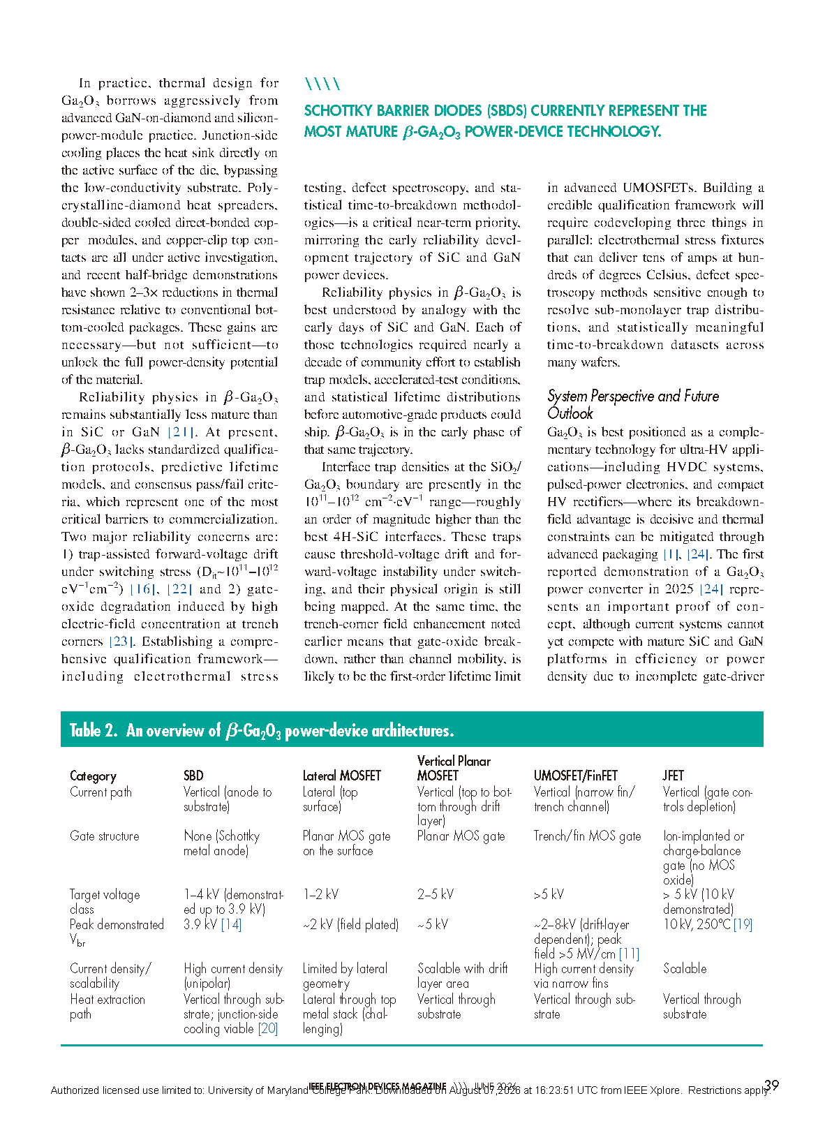
Device architectures including SBD, lateral MOSFET, vertical planar MOSFET, UMOSFET / FinFET and JFET are categorized, with their target voltage class, heat extraction path and technical risks illustrated;
How three material constraints (defect density, anisotropic low thermal conductivity, absence of p-type doping) shape device design is analyzed. Existing challenges in edge termination, thermal management and reliability are concluded;
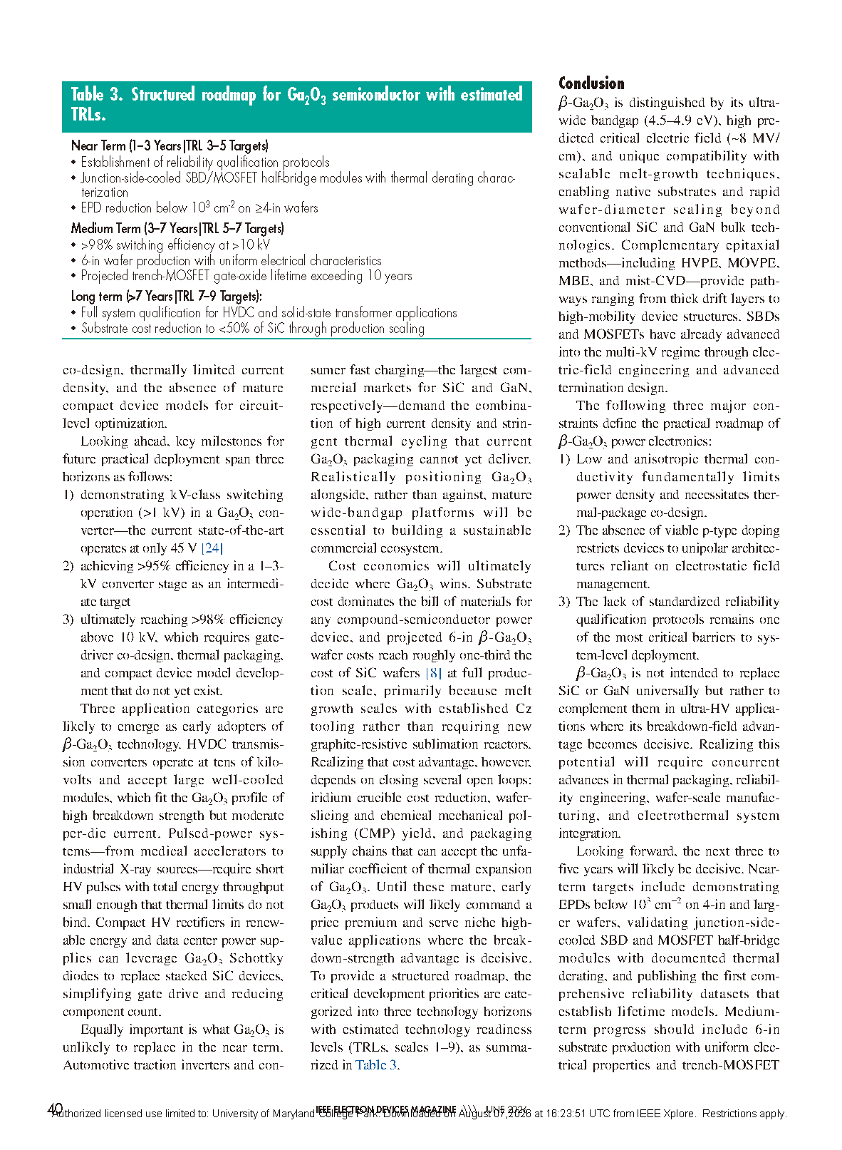
Near-term, medium-term and long-term development milestones with TRL grading are proposed, with practical targets on wafer, device and system levels. This work positions β-Ga₂O₃ as a complementary rather than substituting ultra-HV semiconductor.
Conclusion
β-Ga₂O₃ is distinguished by its ultrawide bandgap (4.5–4.9 eV), high predicted critical electric field (~8 MV/cm), and unique compatibility with scalable melt-growth techniques, enabling native substrates and rapid wafer-diameter scaling beyond conventional SiC and GaN bulk technologies. Complementary epitaxial methods—including HVPE, MOVPE, MBE, and mist-CVD—provide pathways ranging from thick drift layers to high-mobility device structures. SBDs and MOSFETs have already advanced into the multi-kV regime through electric-field engineering and advanced termination design.
The following three major constraints define the practical roadmap of β-Ga₂O₃ power electronics:
1) Low and anisotropic thermal conductivity fundamentally limits power density and necessitates thermal-package co-design.
2) The absence of viable p-type doping restricts devices to unipolar architectures reliant on electrostatic field management.
3) The lack of standardized reliability qualification protocols remains one of the most critical barriers to system-level deployment.
β-Ga₂O₃ is not intended to replace SiC or GaN universally but rather to complement them in ultra-HV applications where its breakdown-field advantage becomes decisive. Realizing this potential will require concurrent advances in thermal packaging, reliability engineering, wafer-scale manufacturing, and electrothermal system integration.
Looking forward, the next three to five years will likely be decisive. Near-term targets include demonstrating EPDs below 10³ cm⁻² on 4-in and larger wafers, validating junction-side-cooled SBD and MOSFET half-bridge modules with documented thermal derating, and publishing the first comprehensive reliability datasets that establish lifetime models. Medium-term progress should include 6-in substrate production with uniform electrical properties and trench-MOSFET gate-oxide lifetimes projected to exceed 10 years at rated stress. Long-term success will require full system qualification for HVDC and solid-state transformer applications as well as a substrate cost trajectory that reaches roughly one-third of the cost of comparable SiC at production volume. None of these milestones is guaranteed, but each represents a tractable engineering problem rather than a fundamental scientific barrier—a distinction that, more than any single performance figure, suggests β-Ga₂O₃ deserves the sustained investment the community is now giving it.
Project Support
This work was financially supported by the "Advanced Semiconductor Technology Research Center" from the Featured Areas Research Center Program within the framework of the Higher Education Sprout Project by the Ministry of Education (MOE) in Taiwan and in part by the National Science and Technology Council (NSTC) Grant 114-2923-E-A49-008MY3; by the Deutsche Forschungsgemeinschaft (DFG, German Research Foundation)—Project PO-2659/1-2; and by the European Community (Europäische Fonds für regionale Entwicklung—EFRE) under Grant 1.8/15.
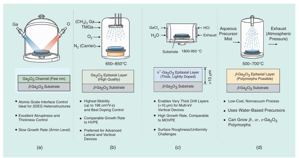
Figure 1. A comparison of common β-Ga₂O₃ epitaxial growth technologies. The diagram highlights four key deposition methods: (a) molecular beam epitaxy (MBE), (b) metal-organic vapor deposition epitaxy (MOVPE), (c) halide vapor-phase epitaxy (HVPE), and (d) Mist-CVD.
DOI:
10.1109/MED.2026.3707419

Instruction
Official Account

Cooperation
Top
