


Researchers from the Xidian University have published a dissertation titled "NH₃ Plasma Surface Treatment in β-Ga₂O₃: Interface Trap Density Reduction and MOSFET Performance Gains" in IEEE Transactions on Electron Devices.
Background
β-phase gallium oxide (β-Ga₂O₃) is an emerging ultra-wide bandgap semiconductor with the potential for low-cost substrate preparation, making it a core candidate material for next-generation power devices. Over the past decade, remarkable progress has been made in the research and development of β-Ga₂O₃ MOSFETs. However, the defects at the dielectric/semiconductor interface have always been the key bottleneck limiting device performance and reliability, leading to threshold voltage shift, large hysteresis, degraded subthreshold swing and other issues. Al₂O₃ has become the mainstream gate dielectric for β-Ga₂O₃ MOSFETs due to its large conduction band offset, moderate permittivity and excellent compatibility with atomic layer deposition. Traditional interface treatment methods such as wet chemical cleaning and post-deposition annealing can only reduce the interface trap density to the order of 10¹² eV⁻¹·cm⁻², which cannot meet the requirements of high-performance devices. Ammonia plasma treatment (NPT) has been verified to have interface passivation effects in Si, GaAs and GaN systems, and the team has previously applied it to β-Ga₂O₃ Schottky barrier diodes and achieved reduced interface states. However, the systematic research of this process in the interface engineering of β-Ga₂O₃ MOSFETs is still blank.
Abstract
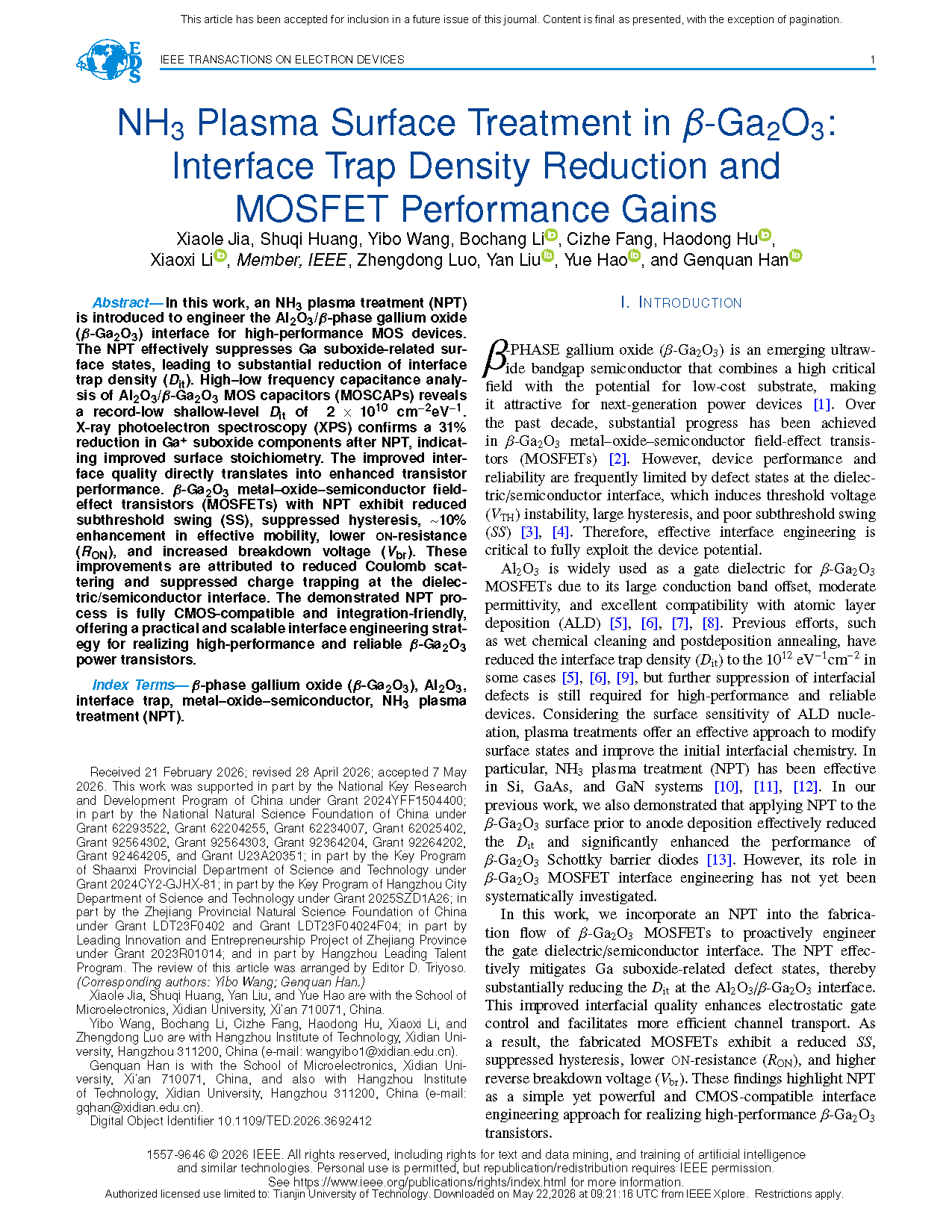
In this work, an NH₃ plasma treatment (NPT) is introduced to engineer the Al₂O₃ / β-phase gallium oxide (β-Ga₂O₃) interface for high-performance MOS devices. The NPT effectively suppresses Ga suboxide-related surface states, leading to substantial reduction of interface trap density (Dit). High–low frequency capacitance analysis of Al₂O₃ / β-Ga₂O₃ MOS capacitors (MOSCAPs) reveals a record-low shallow-level Dit of 2 ×10¹⁰ cm⁻² eV⁻¹. X-ray photoelectron spectroscopy (XPS) confirms a 31% reduction in Ga⁺ suboxide components after NPT, indicating improved surface stoichiometry. The improved interface quality directly translates into enhanced transistor performance. β-Ga₂O₃ metal–oxide–semiconductor field-effect transistors (MOSFETs) with NPT exhibit reduced subthreshold swing (SS), suppressed hysteresis, ∼10% enhancement in effective mobility, lower ON-resistance (RON), and increased breakdown voltage (Vbr). These improvements are attributed to reduced Coulomb scattering and suppressed charge trapping at the dielectric/semiconductor interface. The demonstrated NPT process is fully CMOS-compatible and integration-friendly, offering a practical and scalable interface engineering strategy for realizing high-performance and reliable β-Ga₂O₃ power transistors.
Highlights
NH₃plasma treatment (NPT) is systematically applied to Al₂O₃/β-Ga₂O₃ interface engineering for the first time, achieving a record-low interface trap density of 2×10¹⁰ cm⁻²·eV⁻¹;
XPS confirms that NPT reduces the Ga⁺suboxide component on β-Ga₂O₃ surface by 31%, revealing the interface passivation mechanism at the chemical level;
NPT process simultaneously improves multiple core performances of β-Ga₂O₃MOSFETs: 12.6% reduction in subthreshold swing, 46.5% reduction in hysteresis, ~10% enhancement in effective mobility, lower ON-resistance and higher breakdown voltage;
The process is fully CMOS-compatible with no vacuum break and negligible ion bombardment damage, featuring industrial scalability.
Conclusion
In conclusion, an NPT has been systematically implemented to engineer the β-Ga₂O₃ surface prior to Al₂O₃ deposition, effectively mitigating Ga suboxide-related defects and significantly improving the dielectric/semiconductor interface quality. The Al₂O₃ / β-Ga₂O₃ MOSCAPs exhibit an ultralow shallow-level Dit of 2 ×10¹⁰ cm⁻² eV⁻¹, representing a record-low value for this material system. β-Ga₂O₃ MOSFETs incorporating NPT demonstrate reduced SS, suppressed hysteresis, lower RON, and improved Vbr, collectively indicating strengthened electrostatic control, reduced Coulomb scattering, and enhanced dielectric robustness. As a result, as a CMOS-compatible and integration-friendly surface engineering strategy, NPT provides an effective and scalable pathway toward high-performance and reliable β-Ga₂O₃ power transistors.
Project Support
This work was supported in part by the National Key Research and Development Program of China under Grant 2024YFF1504400; in part by the National Natural Science Foundation of China under Grant 62293522, Grant 62204255, Grant 62234007, Grant 62025402, Grant 92564302, Grant 92564303, Grant 92364204, Grant 92264202, Grant 92464205, and Grant U23A20351; in part by the Key Program of Shaanxi Provincial Department of Science and Technology under Grant 2024CY2-GJHX-81; in part by the Key Program of Hangzhou City Department of Science and Technology under Grant 2025SZD1A26; in part by the Zhejiang Provincial Natural Science Foundation of China under Grant LDT23F0402 and Grant LDT23F04024F04; in part by Leading Innovation and Entrepreneurship Project of Zhejiang Province under Grant 2023R01014; and in part by Hangzhou Leading Talent Program.
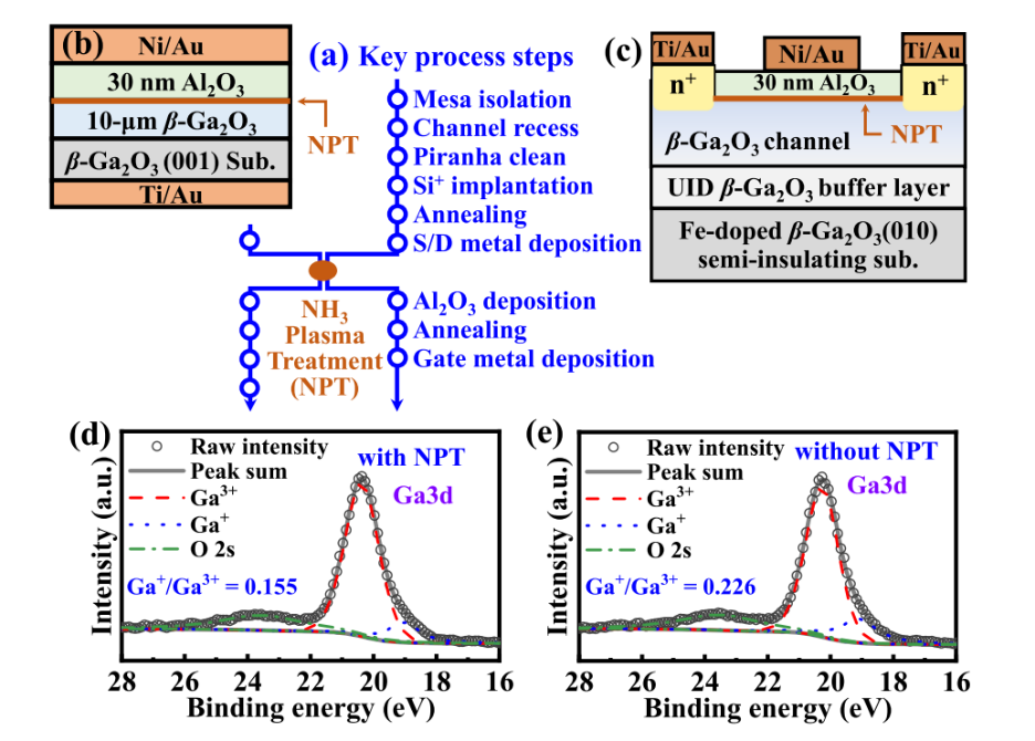
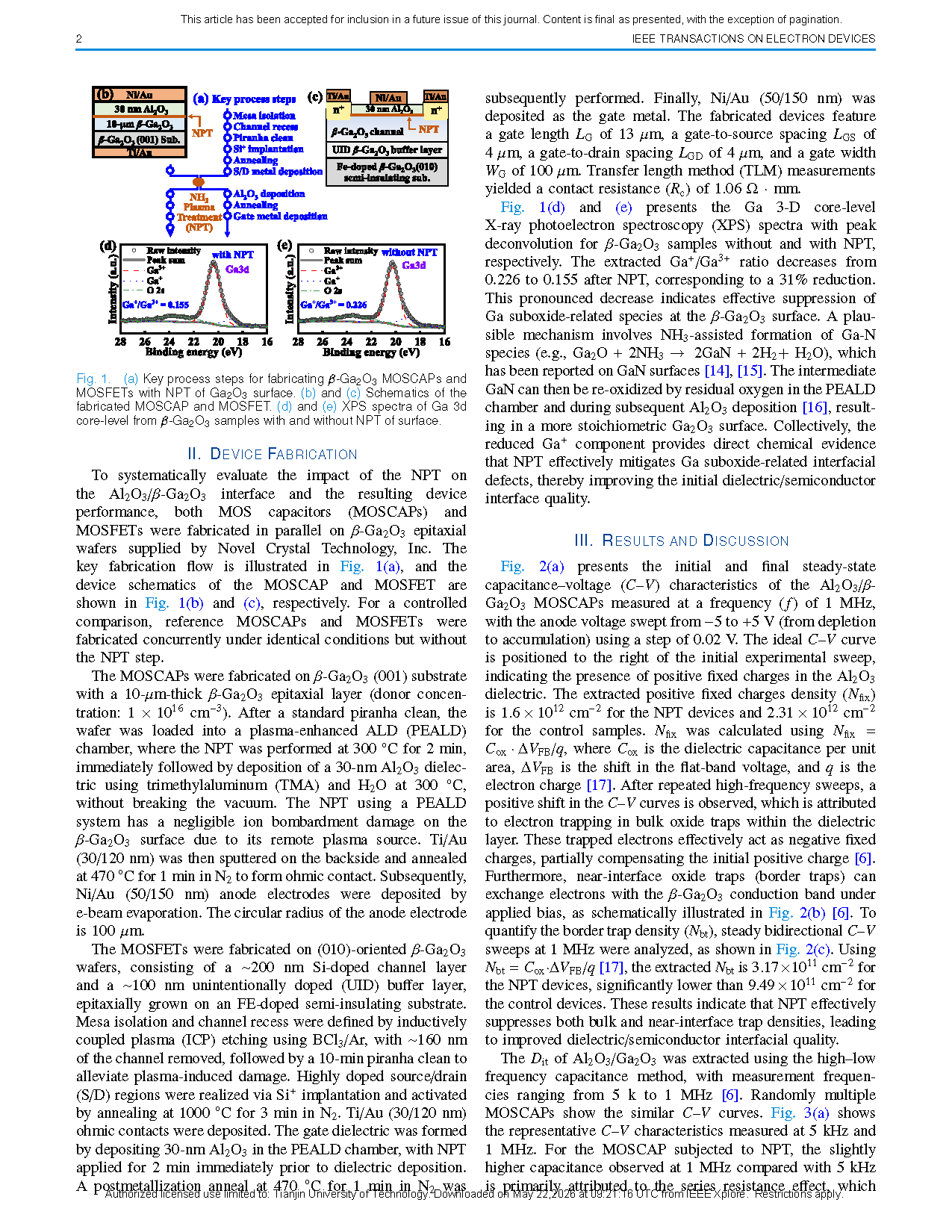
Fig. 1. (a) Key process steps for fabricating β-Ga₂O₃ MOSCAPs and MOSFETs with NPT of Ga₂O₃ surface. (b) and (c) Schematics of the fabricated MOSCAP and MOSFET. (d) and (e) XPS spectra of Ga 3d core-level from β-Ga₂O₃ samples with and without NPT of surface.
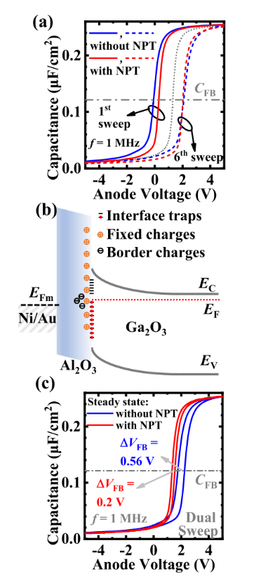
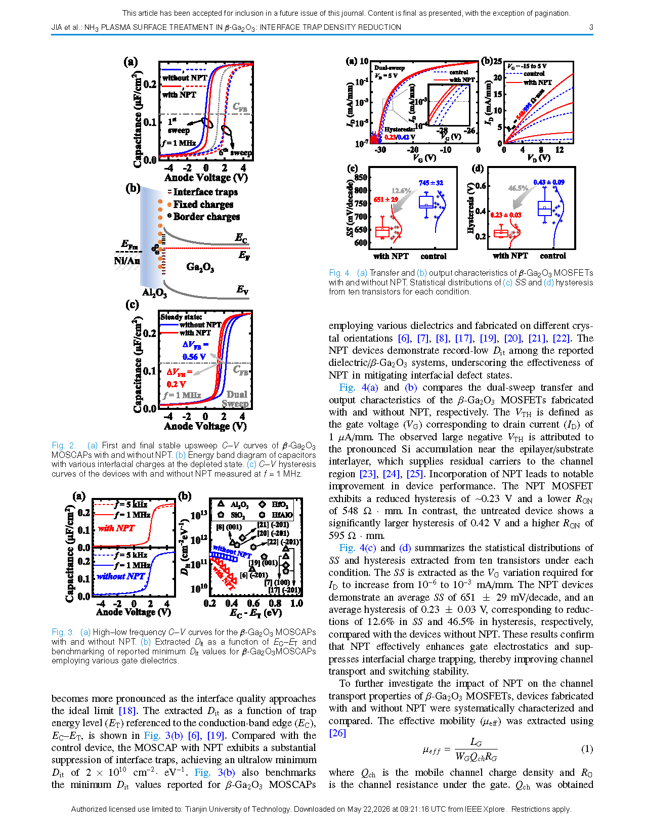
Fig. 2. (a) First and final stable upsweep C–V curves of β-Ga₂O₃ MOSCAPs with and without NPT. (b) Energy band diagram of capacitors with various interfacial charges at the depleted state. (c) C–V hysteresis curves of the devices with and without NPT measured at f=1 MHz.
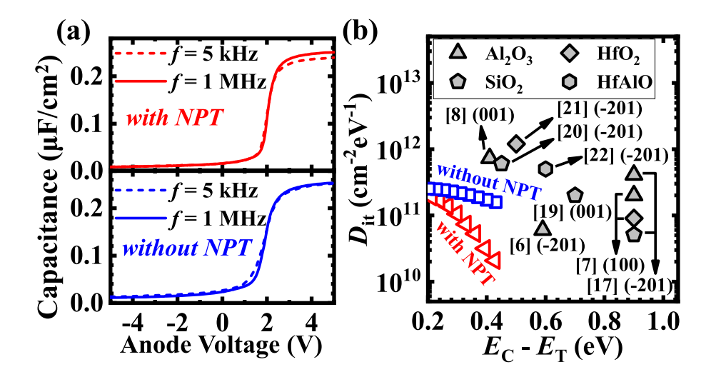
Fig. 3. (a) High–low frequency C–V curves for the β-Ga₂O₃ MOSCAPs with and without NPT. (b) Extracted Dit as a function of EC−ET and benchmarking of reported minimum Dit values for β-Ga₂O₃ MOSCAPs employing various gate dielectrics.
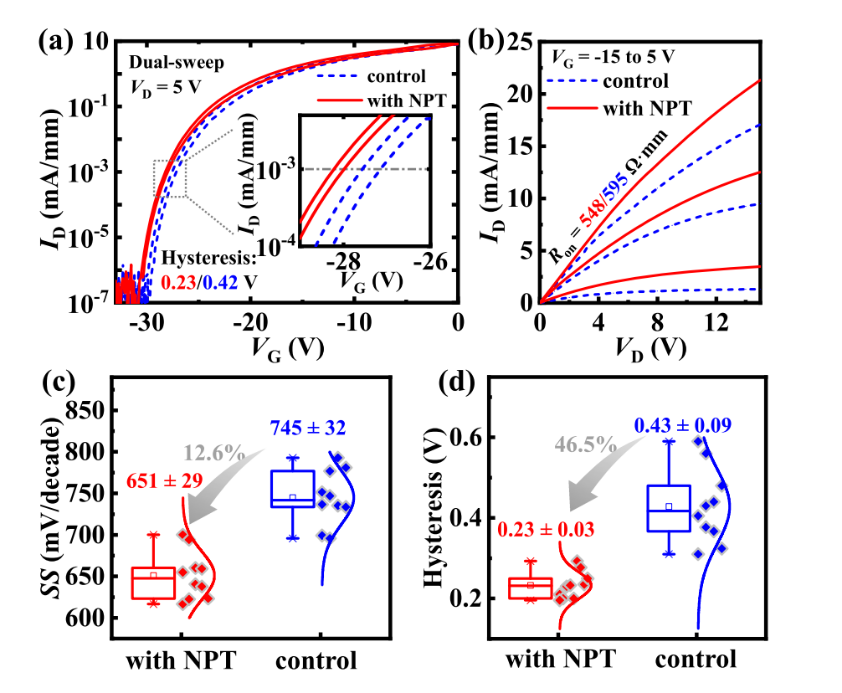
Fig. 4. (a) Transfer and (b) output characteristics of β-Ga₂O₃ MOSFETs with and without NPT. Statistical distributions of (c) SS and (d) hysteresis from ten transistors for each condition.
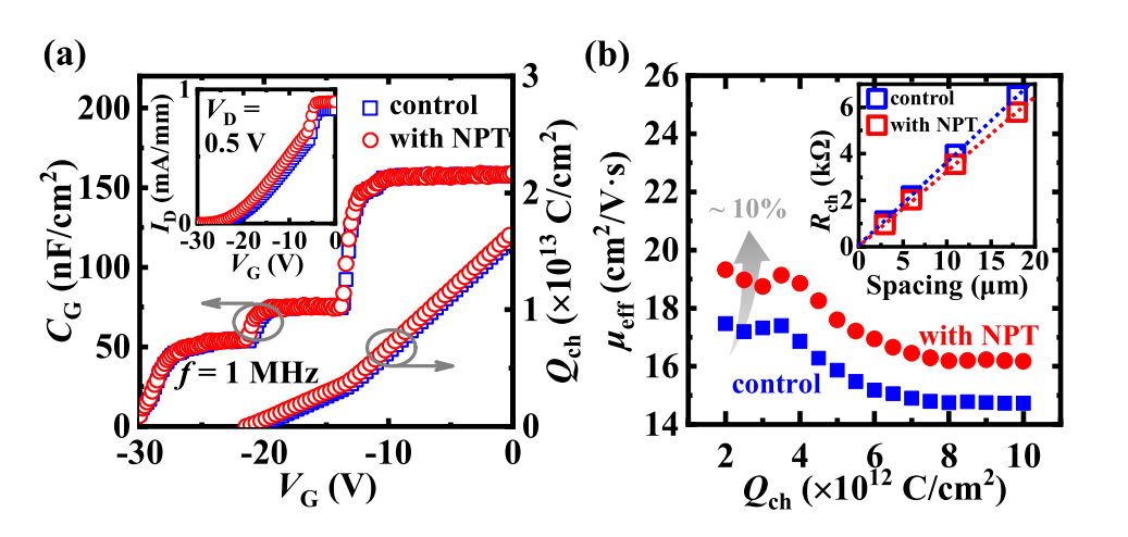
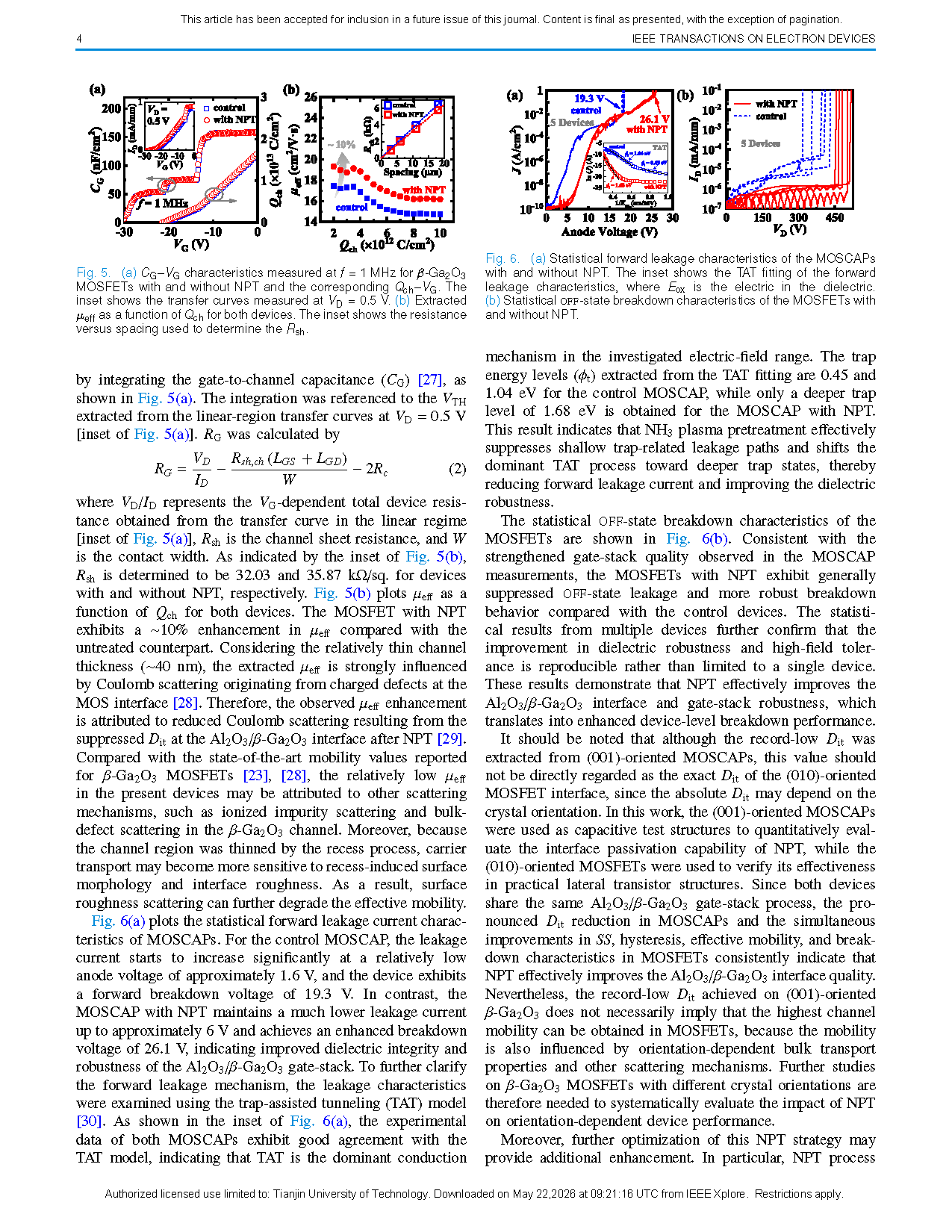
Fig. 5. (a) CG−VG characteristics measured at f=1 MHz for β-Ga₂O₃ MOSFETs with and without NPT and the corresponding Qch−VG. The inset shows the transfer curves measured at VD=0.5 V. (b) Extracted μeff as a function of Qch for both devices. The inset shows the resistance versus spacing used to determine the Rsh.
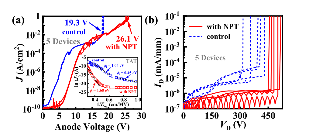
Fig. 6. (a) Statistical forward leakage characteristics of the MOSCAPs with and without NPT. The inset shows the TAT fitting of the forward leakage characteristics, where Eox is the electric in the dielectric. (b) Statistical OFF-state breakdown characteristics of the MOSFETs with and without NPT.
DOI:
10.1109/TED.2026.3692412
Instruction
Official Account

Cooperation
Top
