


β-Ga₂O₃, with a bandgap of approximately 4.8 eV, a breakdown field of approximately 8 MV/cm, and a Baliga figure of merit several times higher than that of SiC, is regarded as a promising candidate for next-generation high-voltage power devices and solar-blind ultraviolet photodetectors. However, its melting point is approximately 1800°C, and it is prone to decomposition and volatilization at high temperatures. In addition, its relatively low thermal conductivity, pronounced anisotropy, and readily cleavable planes impose specific requirements on crystal growth methods. To address the unique characteristics of this material system, Garen Semiconductor has independently developed a dedicated VB crystal-growth system for gallium oxide. This article, the first in the series, introduces the fundamental principles of the vertical Bridgman (VB) method and analyzes its compatibility with β-Ga₂O₃.
01.Basic Principles of the VB Method
After the raw materials are fully melted inside the crucible, the crucible is moved through a thermal field with an axial temperature gradient at a controlled rate. The melt gradually solidifies layer by layer from the bottom upward at the solid–liquid interface, allowing the entire melt to directionally crystallize into a single crystal.
Unlike edge-defined film-fed growth (EFG), which is an “out-of-crucible” crystal growth technique, the VB method is an “in-crucible” growth technique. Benefiting from the confinement provided by the enclosed crucible, VB growth can achieve directional solidification and shaping in a single process without the need for shoulder expansion or diameter-control stages. It also offers greater flexibility in selecting the crystal orientation.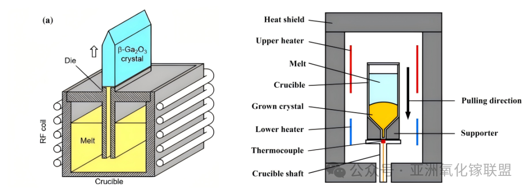
Figure 1. Schematic diagrams of the EFG method (left) and the VB method (right).
02.Compatibility of the VB Method with β-Ga₂O₃
01 Significantly Lower Cost
The EFG method relies on iridium crucibles. However, iridium has a relatively low high-temperature oxidation threshold and can spontaneously oxidize into IrO₂/IrO₃ even at very low oxygen partial pressures (<2 vol%), resulting in significant oxidation and volatilization losses [1]. Combined with the intrinsically high cost of iridium materials, this leads to high consumable costs.
The VB method uses platinum–rhodium alloy crucibles, whose excellent high-temperature oxidation resistance helps reduce both oxidation losses and the risk of impurity introduction.
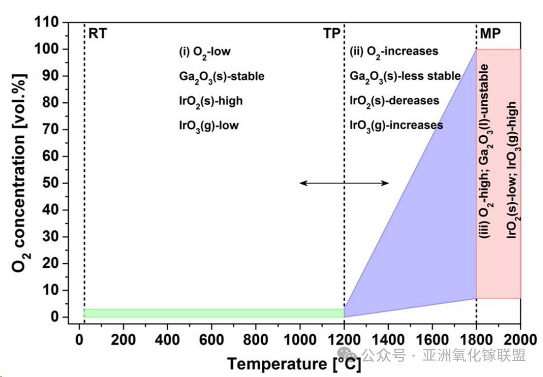
Figure 2. Relationship between iridium loss and temperature.
02 Suppression of Melt Decomposition
The low oxidation threshold of iridium not only leads to material loss but also imposes stringent constraints on the process window. To prevent iridium oxidation, the EFG method must maintain an extremely low oxygen partial pressure. However, such a low oxygen partial pressure further aggravates the thermal decomposition of the crystal. As a result, EFG growth faces a difficult trade-off between suppressing gallium oxide decomposition and minimizing iridium loss, leaving an extremely narrow atmosphere window.
In contrast, the strong oxidation resistance of platinum–rhodium alloy crucibles used in the VB method removes this limitation. VB growth can be carried out in air or even under higher oxygen partial pressures, significantly suppressing thermal decomposition [2] and fundamentally broadening the process window.
03 Higher Growth Yield
β-Ga₂O₃ exhibits pronounced anisotropy and therefore imposes stringent requirements on the rotational symmetry of the thermal field. As a result, “out-of-crucible” growth techniques represented by the EFG method are highly susceptible to defects during the shoulder expansion and constant-diameter growth stages, significantly hindering improvements in yield.
In contrast, the rigid confinement provided by the crucible in the VB method effectively suppresses defects such as dislocations and twins induced by material anisotropy, resulting in a substantially higher growth yield.
04 Uniform and Controllable Thermal Field
The VB method employs resistance heating to establish a thermal field with a hotter upper region and a cooler lower region. This not only avoids the instability associated with the induction heating used in the EFG method, but also effectively suppresses natural convection driven by gravity. As a result, the temperature gradient at the solid–liquid interface is reduced, significantly improving interface stability and thereby reducing thermal stress in the crystal.
Comparative measurements using high-resolution X-ray diffraction (HRXRD) and synchrotron X-ray topography show that VB-grown crystals exhibit a lower X-ray rocking-curve full width at half maximum (FWHM) than EFG-grown crystals [3].
05 Flexible Crystal Orientation
The VB method has successfully produced β-Ga₂O₃ single crystals with (100), (010), and (001) orientations, providing a flexible materials platform for research on orientation-dependent epitaxy and device physics [4]. Hoshikawa et al. were among the early researchers to demonstrate the growth of β-Ga₂O₃ single crystals by the VB method in an air atmosphere [2]. Since then, research on the VB method has gradually shifted from feasibility validation toward equipment development and process stability.
It is worth noting that despite its strong compatibility with β-Ga₂O₃, the research foundation for VB-grown β-Ga₂O₃ remains relatively limited. The number of publicly available studies is significantly smaller than that of the EFG route. Fundamental issues—including thermal-field design principles, dopant transport and uniformity, and defect evolution mechanisms—have yet to be systematically elucidated, leaving substantial room for further research.
03.Advantages of Garen Semiconductor’s VB Growth Equipment
The melting point of Ga₂O₃, at approximately 1800 °C, its sensitivity to oxygen partial pressure, and its requirement for a relatively gentle temperature gradient mean that the equipment itself is an integral part of the growth process. Garen Semiconductor’s VB crystal growth equipment is specifically designed around the thermophysical properties of β-Ga₂O₃, offering four key advantages:
Strong size compatibility
The equipment can flexibly accommodate VB growth of β-Ga₂O₃single crystals in different sizes, without the need for frequent replacement of core components.
High-precision temperature control
Temperature control accuracy reaches ±0.1 °C, with real-time monitoring of key parameters throughout the crystal growth process.
Simple deployment
The equipment does not require additional process-gas supplies, compressed air, cooling water, or other auxiliary infrastructure, simplifying installation and deployment.
Integrated equipment and process solution
Garen Semiconductor provides the corresponding growth processes alongside the equipment, offering an integrated “VB furnace + process package”solution.
Supported by its proprietary equipment platform, Garen Semiconductor has achieved β-Ga₂O₃ single-crystal growth from 2 to 8 inches. The equipment is now available for commercial sale, together with standardized process packages and technical support, and has already been delivered to multiple universities and research institutes. It can support research in areas including crystal-growth mechanisms, dopant control, and defect engineering.
By enabling directional solidification within a crucible, the VB method addresses four key requirements for Ga₂O₃ crystal growth: crucible cost, atmosphere control, thermal stress, and crystal orientation. At the same time, the relatively limited research base leaves considerable room for further academic exploration. However, how to design and maintain an optimal temperature-gradient distribution over extended growth periods remains a key challenge for the engineering development of the VB method.
In the next installment, we will examine the design logic and control strategies of the VB thermal field.
Reference
[1] Z. Galazka, R. Uecker, D. Klimm, et al. Scaling-up of bulk β-Ga₂O₃ single crystals by the Czochralski method [J]. ECS Journal of Solid State Science and Technology, 2017, 6(2): Q3007-Q3011.
[2] K. Hoshikawa, E. Ohba, T. Kobayashi, et al. Growth of β-Ga₂O₃ single crystals using vertical Bridgman method in ambient air [J]. Journal of Crystal Growth, 2016, 447: 36–41.
[3] M. I. Chaman, K. Hoshikawa, S. Sdoeung, et al. High crystal quality of vertical Bridgman and edge-defined film-fed growth β-Ga₂O₃ bulk crystals investigated using high-resolution X-ray diffraction and synchrotron X-ray topography [J]. Japanese Journal of Applied Physics, 2022, 61(5): 055501.
E. Ohba, et al. Growth of (100), (010) and (001) β-Ga₂O₃ single crystals by vertical Bridgman method [J]. Journal of Crystal Growth, 2021, 556: 125990.
About Garen Semiconductor
Hangzhou Garen Semiconductor Co., Ltd. is a global provider of gallium oxide materials and equipment solutions, specializing in the R&D and commercialization of ultra-wide-bandgap semiconductor technologies. The company’s core products include 2–8 inch gallium oxide single crystals and substrates (including the world’s first 8-inch products), vertical Bridgman (VB) gallium oxide crystal growth equipment, and 2–8 inch gallium oxide homoepitaxial wafers (including the world’s first 8-inch products). Garen Semiconductor is dedicated to building a fully integrated “equipment–crystal growth–substrate–epitaxy” industrial ecosystem and providing comprehensive solutions for global customers. The company’s achievements in gallium oxide have been widely recognized and featured by leading media outlets, including People’s Daily, Xinhua News Agency, Science and Technology Daily, Sina Finance, China Blue News, and The Paper.
For more information, please visit the official website: http://garen.cc/
Or contact us:
Mr. Jiang
Phone: +86 159 1871 9807
Email: jiangjiwei@garen.cc
Mr. Xia
Phone: +86 190 1127 8792
Email: xianing@garen.cc
Instruction
Official Account

Cooperation
Top
