


Researchers from Shandong University, Shenzhen Research Institute of Shandong University, Shandong Key Laboratory of Thermal Science and Smart Energy Systems have published a dissertation titled "Heteroepitaxial growth mechanism of α-Ga₂O₃ films via Mist-CVD" in Ceramics International.
Background
Ultra-wide bandgap gallium oxide semiconductors act as core candidates for next-generation power devices and solar-blind ultraviolet photodetectors. Corundum-structured α-Ga₂O₃ features an ultra-wide bandgap of 5.3 eV and high theoretical breakdown electric field, and it shares isomorphic crystal structure with sapphire substrates, which can break the bottleneck of p-type doping of Ga₂O₃, showing great potential in high-voltage power chips and deep-UV imaging devices. Conventional epitaxial technologies such as MBE, HVPE and MOCVD rely on expensive vacuum equipment and cannot realize large-area mass production. Mist chemical vapor deposition (Mist-CVD) uses atmospheric-pressure liquid precursors with low cost and large-area deposition capability, which is an industrialized growth route for α-Ga₂O₃. Existing Mist-CVD researches only optimize static parameters like growth temperature and atomization frequency, without systematic analysis of thickness-dependent evolution of crystallinity, surface morphology and optical bandgap. The evolution of lattice mismatch-induced residual strain with film thickness remains unclear, and there lacks a complete segmented kinetic growth framework, which restricts the tailored growth of α-Ga₂O₃ films for diverse functional devices, forming a critical technical gap for mass production of Mist-CVD-based Ga₂O₃ devices.
Abstract
Gallium oxide (Ga₂O₃), as an ultrawide-bandgap semiconductor, is emerging as a viable candidate for next-generation power electronics and solar-blind UV detection. However, diverse device architectures impose distinct requirements on film thickness, which strongly influences the structural and optoelectronic properties. To explicitly clarify these thickness-dependent dynamic effects and guide the tailored design of specific devices, we systematically investigate α-Ga₂O₃ films grown via mist chemical vapor deposition (Mist-CVD) across a broad thickness range (17-4846 nm). The films exhibit a stable growth rate (~ 400 nm h⁻¹) in a three-dimensional (3D) island mode. Based on the thickness-dependent evolution of film properties, we delineate this kinetic process into three distinct stages: (I) Nucleation and Coalescence (<400 nm): Defect annihilation and crystalline-quality improvement, evidenced by the narrowing of the XRD rocking-curve FWHM from 266 to ~45 arcsec, mainly account for the initial bandgap blue-shift to 5.32 eV. (Ⅱ) Island Coarsening (400-1400 nm): As islands continuously coarsen to a mature state (RMS ~4 nm), residual thermal tensile strain is identified as an important factor contributing to the progressive bandgap red-shift. (III) Dynamic Steady State (>1400 nm): Morphology and crystal quality stabilize, while residual thermal tensile strain further contributes to bandgap narrowing toward 5.16 eV. Notably, we identify ~400 nm as an optimal thickness that balances structural and optical properties. This work establishes a three-stage kinetic framework for heteroepitaxy and provides useful guidance for the thickness-tailored design of next-generation devices.
Highlights
Achieved α-Ga₂O₃epitaxy from 17 nm to 4.8 μm at ~ 400 nm h⁻¹.
Decoupled the thickness-driven evolution of structural and optical properties.
Proposed a three-stage growth model governed by distinct physical mechanisms.
Identified ~400 nm to optimally balance crystallinity, morphology, and bandgap.
Conclusion
This study systematically investigates the thickness-dependent heteroepitaxy of α-Ga₂O₃ films grown by Mist-CVD over a broad thickness range from 17 nm to 4.8 μm. We demonstrate that epitaxial thickness is not merely a geometric output, but a key tunable parameter for regulating the surface morphology, crystalline quality, and optical properties. To elucidate the underlying physical mechanisms governing this process, we establish a comprehensive three-stage kinetic framework. The system evolves through three distinct regimes: an initial nucleation and coalescence stage characterized by defect annihilation and crystalline-quality improvement, an intermediate island-coarsening stage accompanied by the gradual stabilization of surface morphology and crystalline quality, and a final dynamic steady-state stage in which residual thermal tensile strain becomes increasingly relevant to the bandgap narrowing in thicker films. By mapping this thickness-dependent evolution, the model identifies a thickness window near 400 nm. At this thickness, the film maintains relatively low surface roughness while achieving improved crystalline quality and the widest optical bandgap among the investigated samples. Consequently, the structure-property-thickness relationships established in this work provide useful mechanistic guidance for the thickness-tailored design of α-Ga₂O₃ films for future power electronic and solar-blind ultraviolet optoelectronic devices.
Project Support
This work was supported by the Taishan Industrial Experts Program, Shandong Provincial Natural Science Foundation (No. R2025ZD32), the China Postdoctoral Science Foundation (No. 2025T180160), the Postdoctoral Innovation Program of Shandong Province (No. SDCX-ZG-202502013), the Shenzhen Fundamental Research Program (Nos. JCYJ20240813101231040, JCYJ20250604124217023), and the Guangdong Basic and Applied Basic Research Foundation (Nos. 2025A1515012590, 2026A1515010052).
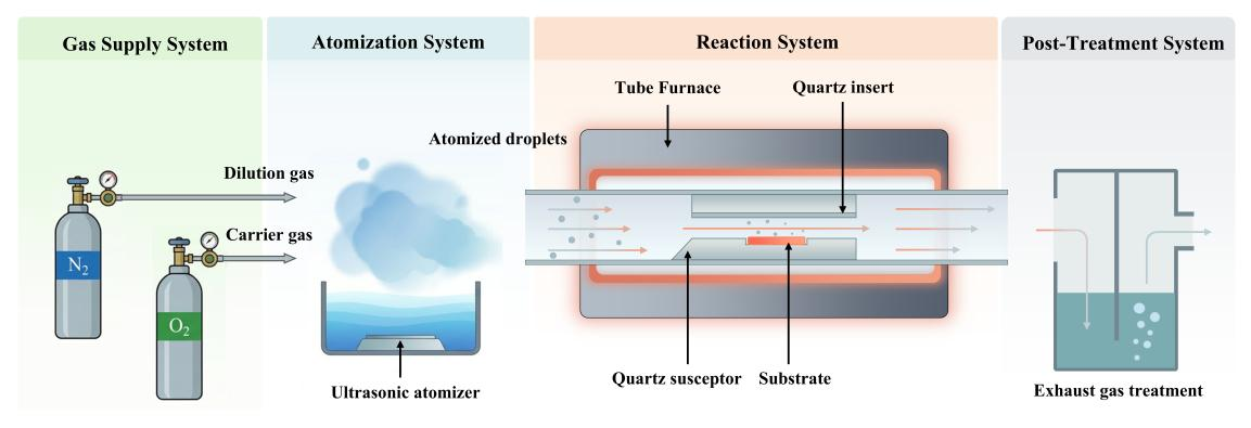
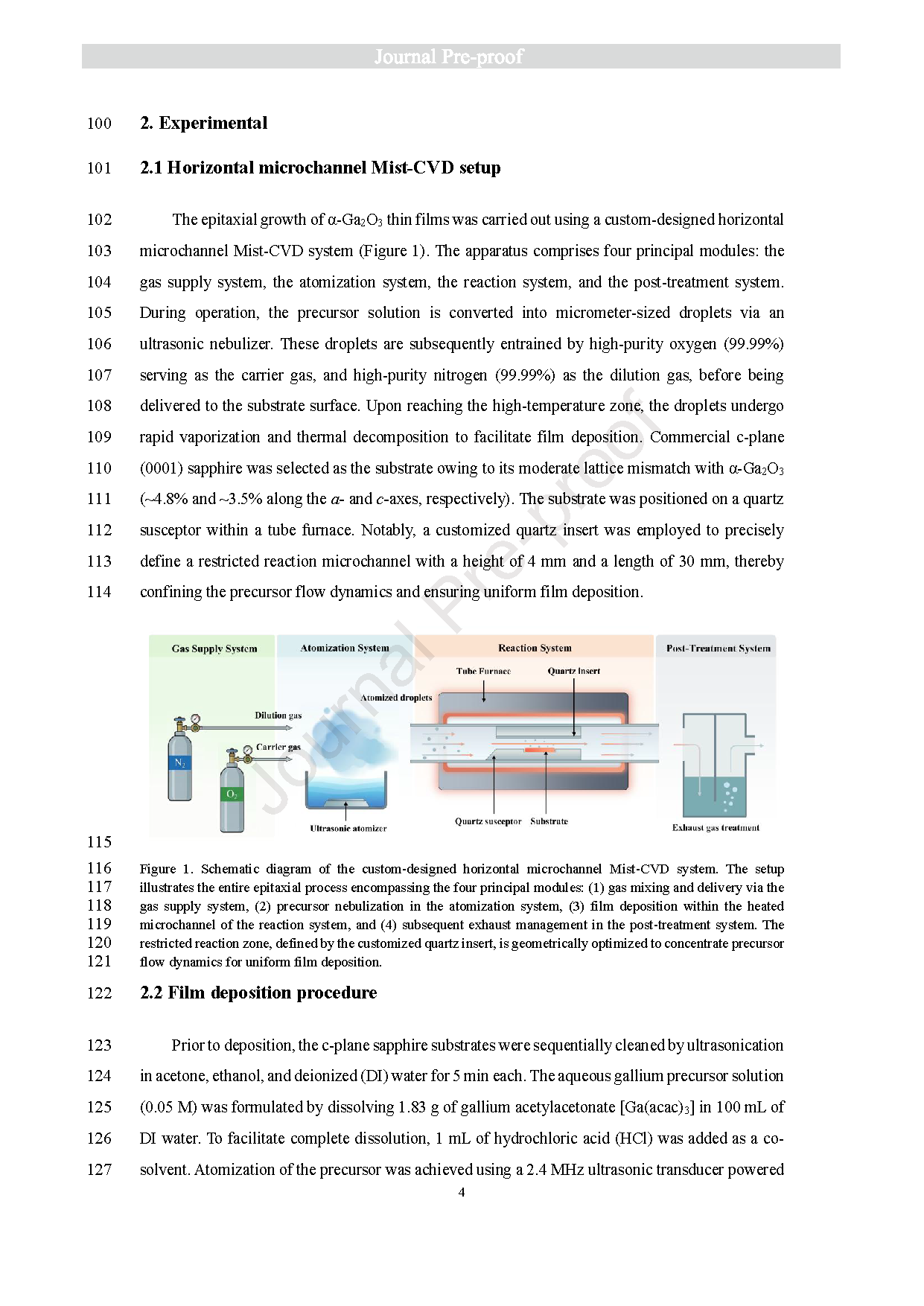
Figure 1. Schematic diagram of the custom-designed horizontal microchannel Mist-CVD system. The setup illustrates the entire epitaxial process encompassing the four principal modules: (1) gas mixing and delivery via the gas supply system, (2) precursor nebulization in the atomization system, (3) film deposition within the heated microchannel of the reaction system, and (4) subsequent exhaust management in the post-treatment system. The restricted reaction zone, defined by the customized quartz insert, is geometrically optimized to concentrate precursor flow dynamics for uniform film deposition.
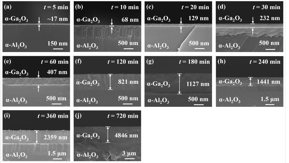
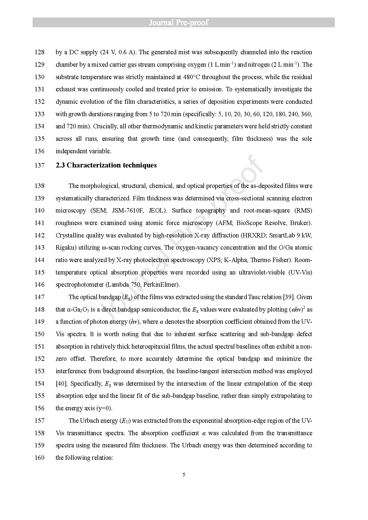
Figure 2. Cross-sectional SEM images tracking the vertical thickness evolution of α-Ga₂O₃ films grown on sapphire substrates from (a) 5 min to (j) 720 min. The annotated thickness values, measured at the center of each sample, demonstrate a controllable geometric scaling from an ultra-thin initial layer (~17 nm) to a micrometer-scale thick film (~4.85 μm).
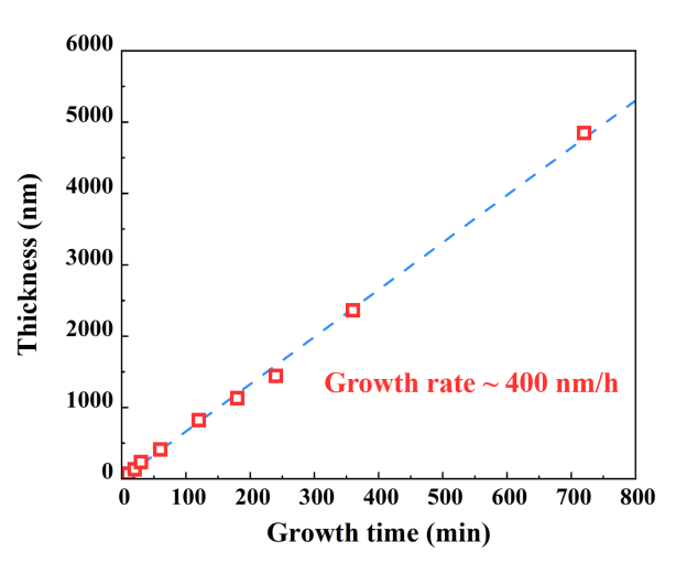
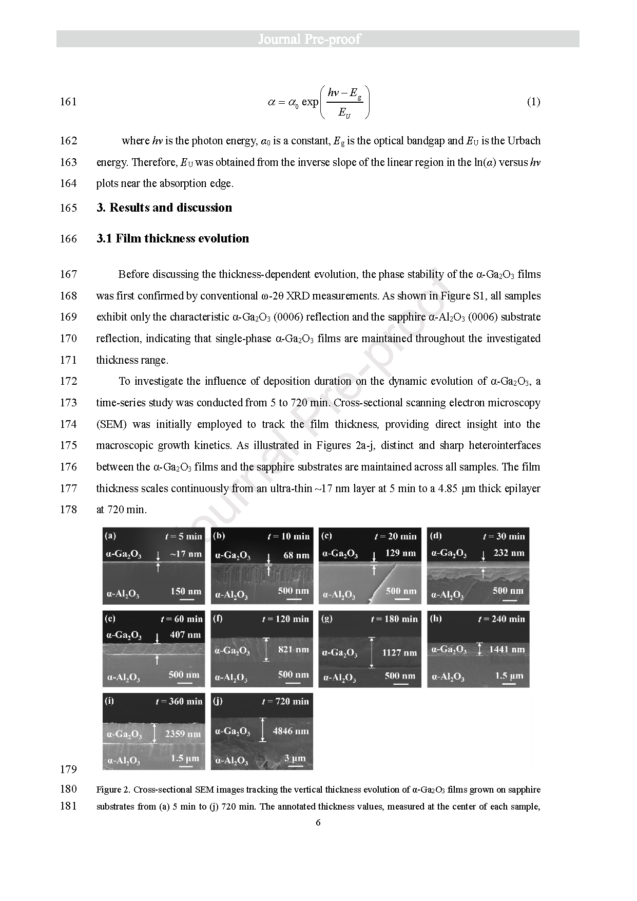
Figure 3. Evolution of α-Ga₂O₃ film thickness as a function of growth time. A linear fit for growth times ≥ 10 min reveals a stable growth rate of ~ 400 nm h⁻¹. The discernible downward deviation of the 5-min sample from this linear trend reflects a transient, nucleation-limited regime prior to complete substrate coverage.
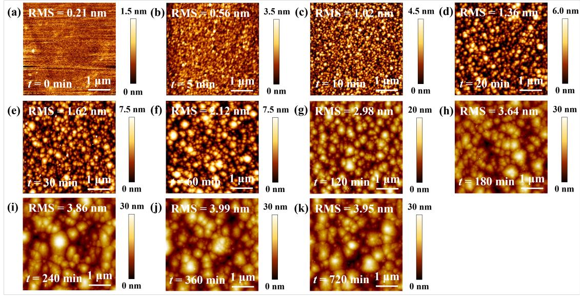
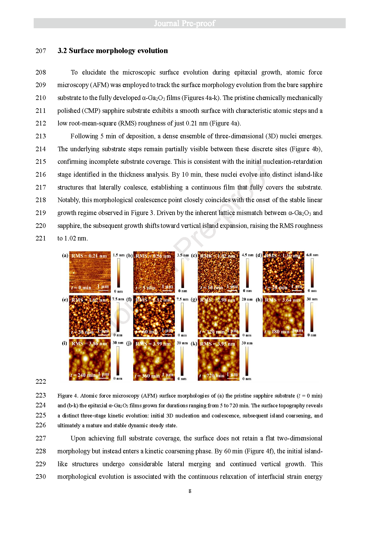
Figure 4. Atomic force microscopy (AFM) surface morphologies of (a) the pristine sapphire substrate (t=0 min) and (b-k) the epitaxial α-Ga₂O₃ films grown for durations ranging from 5 to 720 min. The surface topography reveals a distinct three-stage kinetic evolution: initial 3D nucleation and coalescence, subsequent island coarsening, and ultimately a mature and stable dynamic steady state.
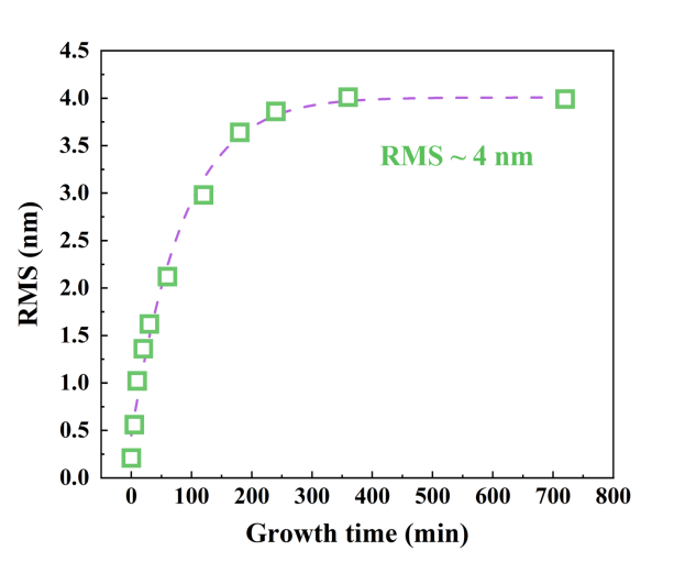
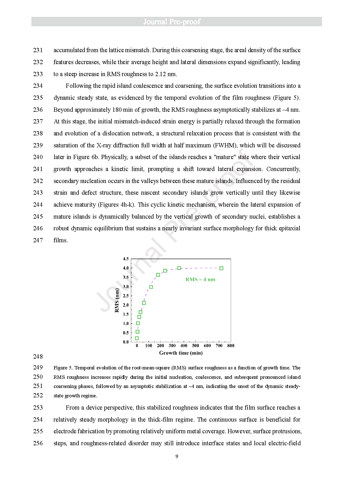
Figure 5. Temporal evolution of the root-mean-square (RMS) surface roughness as a function of growth time. The RMS roughness increases rapidly during the initial nucleation, coalescence, and subsequent pronounced island coarsening phases, followed by an asymptotic stabilization at ~4 nm, indicating the onset of the dynamic steady-state growth regime.
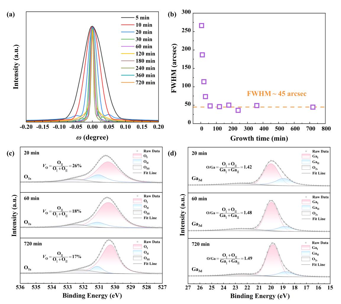
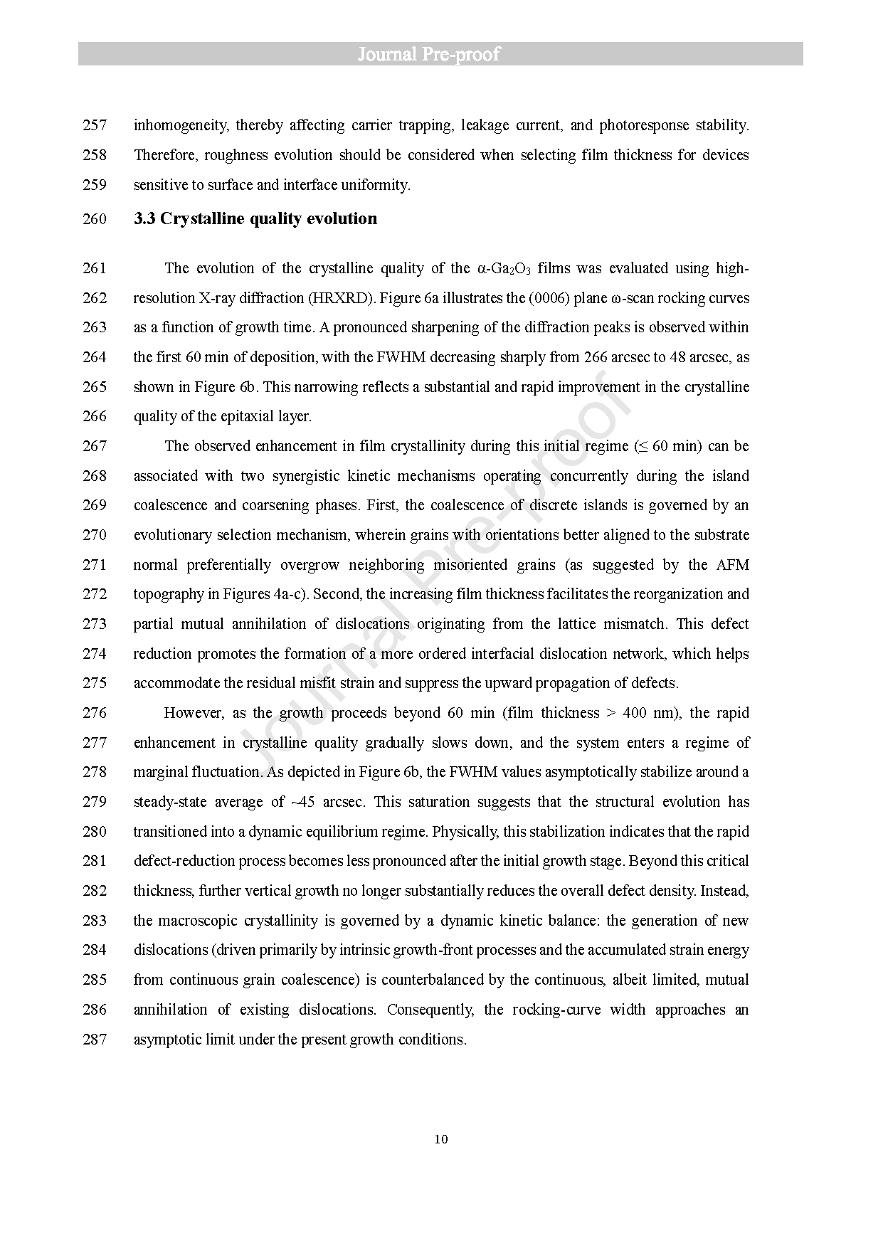
Figure 6. (a) HRXRD ω-scan rocking curves of the α-Ga₂O₃ (0006) plane for films grown at varying durations. (b) The corresponding FWHM values as a function of growth time, revealing a rapid initial improvement in crystalline quality followed by an asymptotic stabilization at a steady-state value of ~45 arcsec. (c) High-resolution O 1s XPS spectra of representative α-Ga₂O₃ films grown for 20, 60, and 720 min. (d) High-resolution Ga 3d XPS spectra of the same representative films.
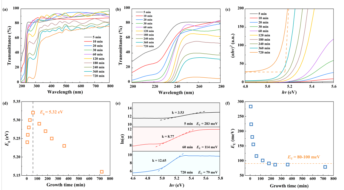
Figure 7. Optical properties, bandgap evolution, and Urbach energy analysis of the α-Ga₂O₃ films. (a) UV-Vis transmittance spectra of the α-Ga₂O₃ films grown for different durations. (b) Enlarged view of the ultraviolet absorption-edge region. (c) Tauc plots, (αhv)² versus hv, used to extract the optical bandgap Eg. (d) Evolution of the optical bandgap Eg as a function of growth time, showing an initial blue-shift followed by a gradual red-shift. (e) Representative ln (α)-hv plots and linear fits in the Urbach absorption-edge region for the films grown for 5, 60, and 720 min. (f) Evolution of the Urbach energy EU as a function of growth time.
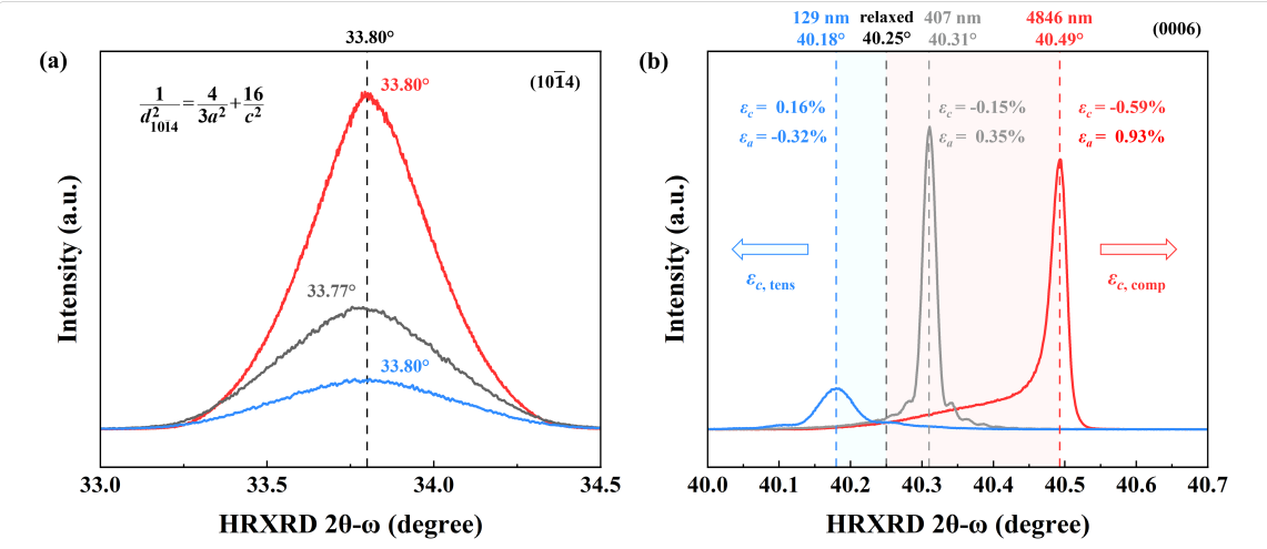
Figure 8. HRXRD peak-position analysis and residual strain evolution of α-Ga₂O₃ films with different thicknesses. (a) Asymmetric (10-14) HRXRD 2θ-ω scans of representative α-Ga₂O₃ films with thicknesses of 129, 407, and 4846 nm, used to evaluate the in-plane a-axis lattice parameter according to the hexagonal lattice relation. (b) Symmetric (0006) HRXRD 2θ-ω scans of the same representative films, used to extract the out-of-plane c-axis lattice parameter. The dashed lines indicate the measured peak positions and the relaxed α-Ga₂O₃ reference position. The extracted strain values show a transition from slight c-axis expansion with in-plane compression in the thinner film to c-axis contraction with in-plane tensile strain in the thick film, indicating thickness-dependent residual strain evolution.
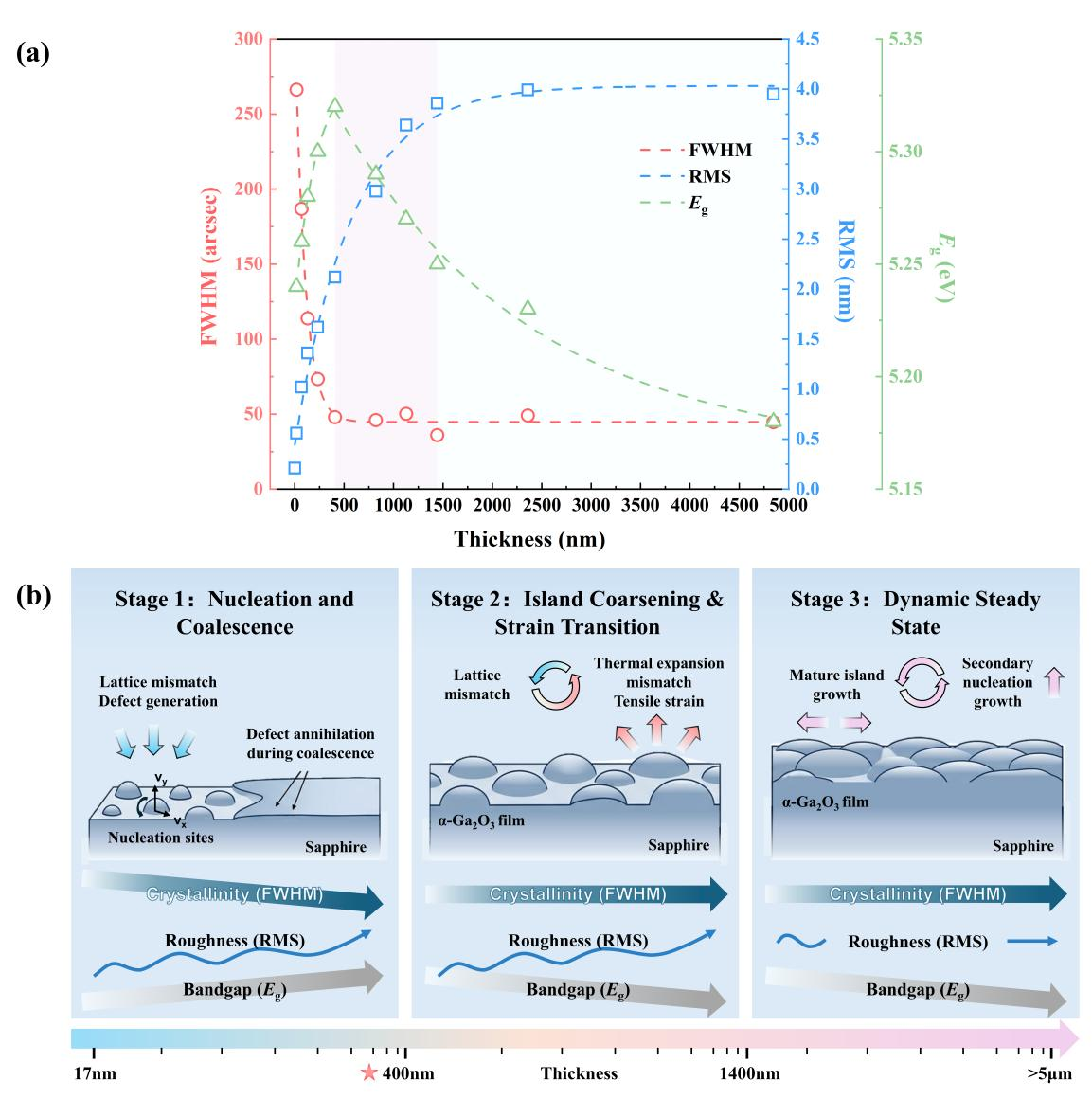
Figure 9. Thickness-driven growth kinetics and property evolution of the α-Ga₂O₃ films. (a) Unified multi-parameter plot correlating crystalline quality (FWHM), surface roughness (RMS), and optical bandgap (Eg) with film thickness. (b) Schematic illustration of the proposed three-stage kinetic growth model. Since the film thickness increases nearly linearly with growth time after the initial nucleation stage, thickness is used as the main coordinate to correlate the experimental property evolution with the underlying growth mechanisms. Stage I, Nucleation and Coalescence, is characterized by rapid island coalescence, defect annihilation, and crystalline-quality improvement, leading to an initial bandgap blue-shift. Stage II, Island Coarsening, involves continuous island coarsening and the gradual stabilization of surface morphology and crystalline quality, accompanied by the onset of bandgap red-shift. Stage III, Dynamic Steady State, is characterized by nearly stabilized surface morphology and crystalline quality, while residual thermal tensile strain further contributes to bandgap narrowing in the thick-film regime. The residual-strain-related pathway shown in this schematic represents a proposed interpretation supported by HRXRD peak-position analysis, rather than an exclusive mechanism.
DOI:
doi.org/10.1016/j.ceramint.2026.08.065


Instruction
Official Account

Cooperation
Top
