


Researchers from Xi’an Jiaotong University, Xi’an Institute of Optics and Precision Mechanics Chinese Academy of Sciences, University of Chinese Academy of Sciences, Shaanxi Provincial Key Laboratory of Electronic Devices and Advanced Chips, Xi’an Key Lab of Micro-nano Electronics and System Integration, ZhongKe Atomically Precise Manufacturing Technology Co Ltd. have published a dissertation titled "Enhanced secondary electron yield of magnetron sputtered Ga₂O₃ ultra-wide bandgap films via high-temperature annealing and AlN surface modification" in Applied Surface Science.
Background
Vacuum photodetectors such as image intensifiers and photomultiplier tubes rely on secondary electron emission (SEE) for signal multiplication, and high secondary electron yield (SEY) materials serve as core dynode layers which determine signal-to-noise ratio of weak light imaging and single photon detection. Traditional MgO and Al₂O₃ dynode materials suffer slow electron replenishment and severe surface charging, leading to structural breakdown during long-term operation. Monoclinic β-Ga₂O₃ ultra-wide bandgap semiconductor owns a 4.6–4.9 eV bandgap and widely tunable resistivity from 10⁻² to 10⁶ Ω・cm, capable of rapidly dissipating surface charge, with excellent thermal and moisture resistance, which makes it ideal for next-generation SEE dynode materials. Existing researches on Ga₂O₃ SEE performance have obvious limitations: as-deposited sputtered films contain massive carbon contaminants and intrinsic oxygen vacancies, leading to high electron escape barrier and low pristine SEY of only 2.54. Single high-temperature annealing can merely slightly improve emission capacity, lacking synergistic AlN surface modification strategy with low electron affinity. Previous literatures only investigate annealing or coating separately, without systematic quantitative analysis on combined process including annealing, AlN deposition and Ar⁺ sputtering. No precise fabrication route for 4 nm quasi-continuous AlN capping layer is reported, and the modulation mechanism of interfacial Al-O-N hybrid phases on secondary electron escape remains unclear, forming a major research gap for mass production of high-performance vacuum electron multipliers.
Abstract
Gallium oxide (Ga₂O₃ ) semiconductor, possessing an ultra-wide bandgap, combines strong secondary electron emission (SEE) capabilities with controllable electrical conductivity. Hence, Ga₂O₃ is supposed to find application in dynodes achieving electron multiplication and charge replenishment. In this work, Ga₂O₃ films were deposited by magnetron sputtering, and high-temperature annealing was used to modulate SEE yield (SEY). Experimental results indicate the 1000 °C annealing in oxygen atmosphere enhances the crystallinity of Ga₂O₃ films and partly eliminates the surface organic contamination, then improves film’s maximum SEY (δₘ ) from 2.54 to 3.21. After coating AlN thin film, which possesses low electron affinity, on Ga₂O₃ sample, surface condition and SEY were further improved. Elemental analysis indicates that following the deposition of AlN, Al element exists on the surface in three forms: Al-N, Al-O, and Al-O-N. And δₘ increased from 2.54 to 3.29. Following annealing and Ar⁺ sputtering, organic contaminants were further removed, restoring the pristine AlN/Ga₂O₃ layer structure. SEY was further enhanced, the AlN-modified Ga₂O₃ sample raised δₘ to 3.35 after annealing, and to 3.44 after annealing and Ar⁺ sputtering. The ultra-wide bandgap Ga₂O₃ material demonstrate promising potential as practical SEE materials for vacuum electron multiplication applications. Moreover, this work provides a valuable reference for expanding SEE applications of other ultra-wide bandgap materials.
Highlights
Propose dual optimization strategy combining high-temperature oxygen annealing and ultrathin AlN surface modification to boost SEY of magnetron sputtered β-Ga₂O₃ films.
Verify that 1000 ℃ oxygen annealing improves crystallinity and removes surface carbon impurities, δₘ rises from 2.54 to 3.21 for bare Ga₂O₃ film.
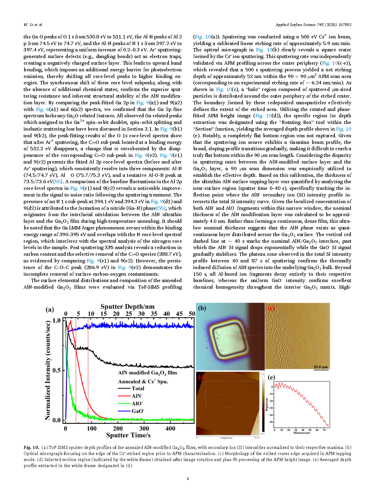
Reveal three Al-containing interfacial phases (Al-N, Al-O, Al-O-N) formed after AlN coating, and realize δₘ =3.29 for AlN-modified sample.
Achieve cumulative 35.4% SEY enhancement via sequential annealing+AlN deposition+Ar⁺ sputtering, final maximum δₘ up to 3.44.
Conclusion
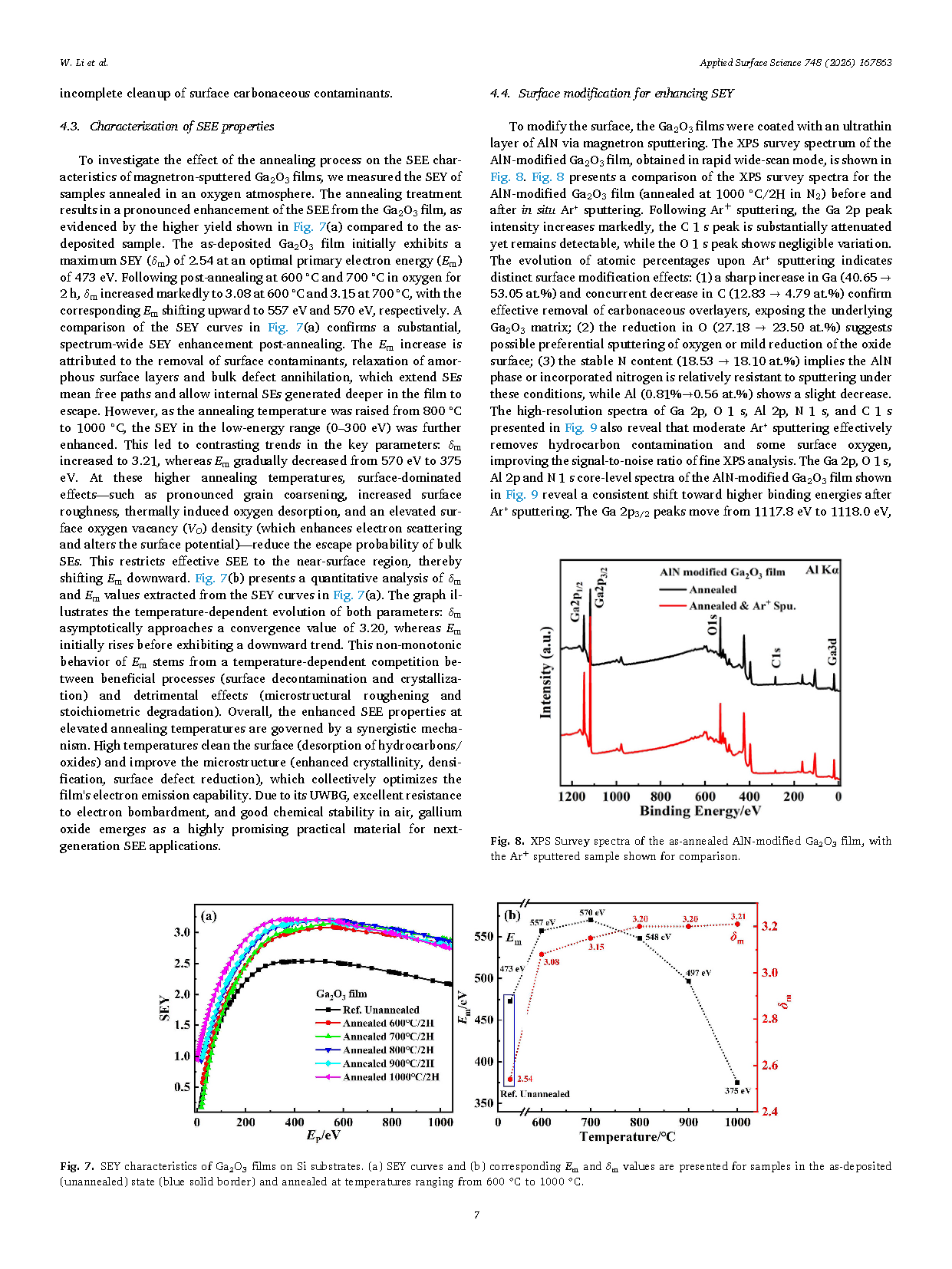
In summary, Ga₂O₃ films were successfully deposited onto low-resistivity n-Si(100) substrates via RF magnetron sputtering, and their SEE performance was comprehensively engineered through post-deposition thermal treatment and AlN surface modification. The as-deposited Ga₂O₃ films of 350 nm were used for surface-sensitive SEY measurements, whereas thicker variants (approximately 1 μm) were synthesized exclusively to ensure sufficient signal intensity for XRD and EDS analyses. High-temperature thermal treatment at 1000 ◦C induced profound structural densification within the matrix, as macroscopically underscored by a 16%-18% contraction in film thickness relative to the as-deposited state. Meanwhile, annealing increased the average grain diameter by 8.7% (from 41.1 nm to 44.7 nm) and the median by 8.9% (from 32.6 nm to 35.5 nm). While the β-Ga₂O₃ phase emerged following high-temperature O₂ annealing (600-1000 °C), substrate-related spectral features were simultaneously resolved in the XRD patterns. Quantitative EDS profiling revealed a sub-stoichiometric Ga:O atomic ratio of 2:2.84 post-annealing. High-temperature annealing systematically improved the δₘ of the Ga₂O₃ films from 2.54 to 3.21, representing a 26.3% enhancement. Furthermore, surface modification via a 4.0 nm AlN nominal layer boosted the low-energy emission regime, shifting δₘ from 2.54 to 3.29 and reducing the Eₘ from 473 eV to 306 eV. Through the synergistic optimization of AlN modification and post-annealing, the δₘ was successfully elevated to 3.35.
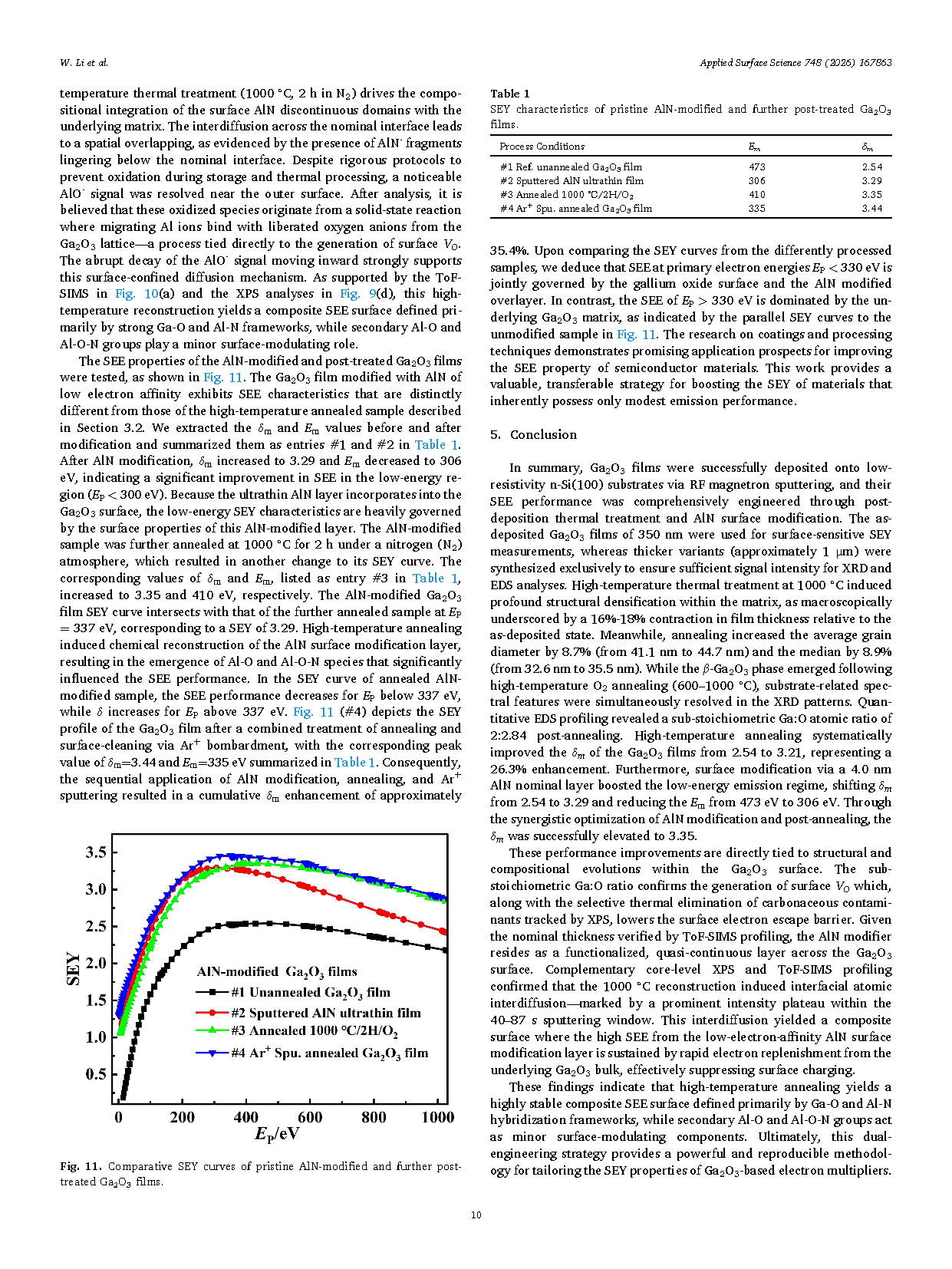
These performance improvements are directly tied to structural and compositional evolutions within the Ga₂O₃ surface. The sub-stoichiometric Ga:O ratio confirms the generation of surface VO which, along with the selective thermal elimination of carbonaceous contaminants, lowers the surface electron escape barrier. Given the nominal thickness verified by ToF-SIMS profiling, the AlN modifier resides as a functionalized, quasi-continuous layer across the Ga₂O₃ surface. Complementary core-level XPS and ToF-SIMS profiling confirmed that the 1000 ◦C reconstruction induced interfacial atomic interdiffusion—marked by a prominent intensity plateau within the 40–87 s sputtering window. This interdiffusion yielded a composite surface where the high SEE from the low-electron-affinity AlN surface modification layer is sustained by rapid electron replenishment from the underlying Ga₂O₃ bulk, effectively suppressing surface charging.
These findings indicate that high-temperature annealing yields a highly stable composite SEE surface defined primarily by Ga-O and Al-N hybridization frameworks, while secondary Al-O and Al-O-N groups act as minor surface-modulating components. Ultimately, this dual-engineering strategy provides a powerful and reproducible methodology for tailoring the SEY properties of Ga₂O₃ -based electron multipliers. This practical scheme can be universally extended to enhance other UWBG material systems, expanding the library of robust material options for next-generation high-power electronic, RF, and electron multiplication devices.
Project Support
Project supported by the Integrated Circuit Manufacturing Materials Innovation Consortium Project of Gansu Province (Grant No. 25ZDGE004), the Fundamental Research Funds for the Central Universities (Grant. No. xzy012025052), the National Natural Science Foundation of China (Grant. No. 62101425), the Major scientific research instrument development project of National Natural Science Foundation of China (Grant No. 52127817) and the Shenzhen Science and Technology Program (Grant No. KJZD20231023100501003).
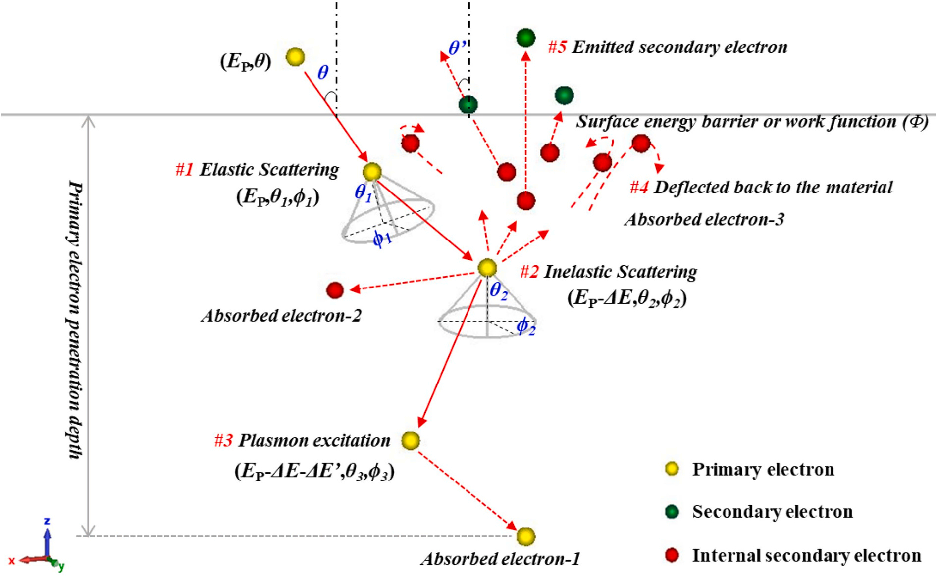
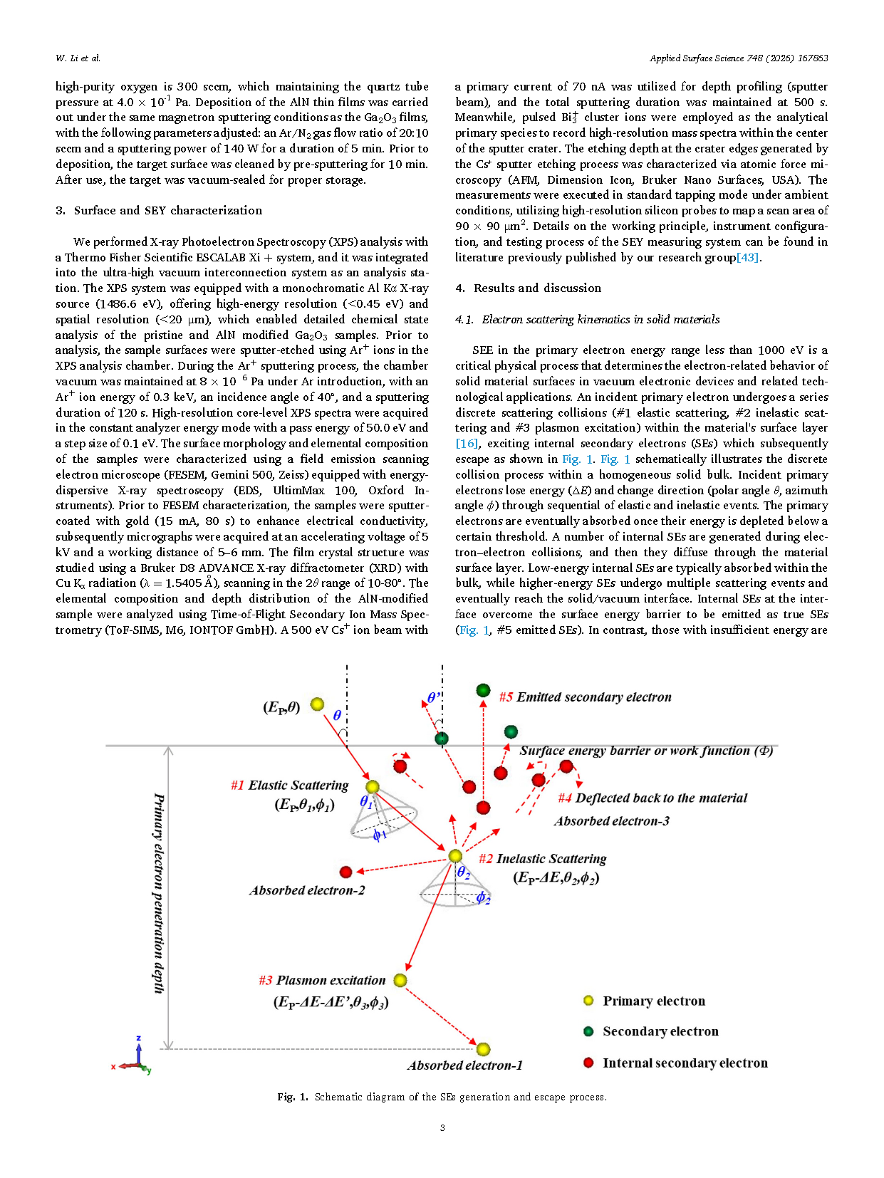
Fig. 1. Schematic diagram of the SEs generation and escape process.
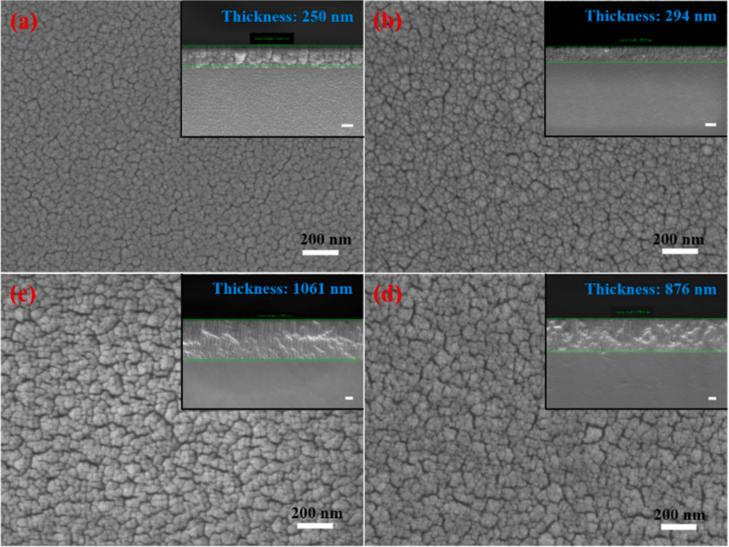
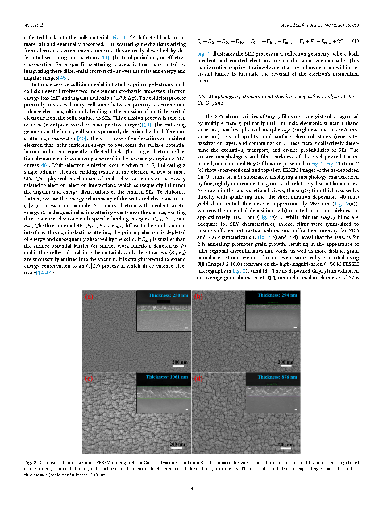
Fig. 2. Surface and cross-sectional FESEM micrographs of Ga₂O₃ films deposited on n-Si substrates under varying sputtering durations and thermal annealing: (a, c) as-deposited (unannealed) and (b, d) post-annealed states for the 40 min and 2 h depositions, respectively. The insets illustrate the corresponding cross-sectional film thicknesses (scale bar in insets: 200 nm).
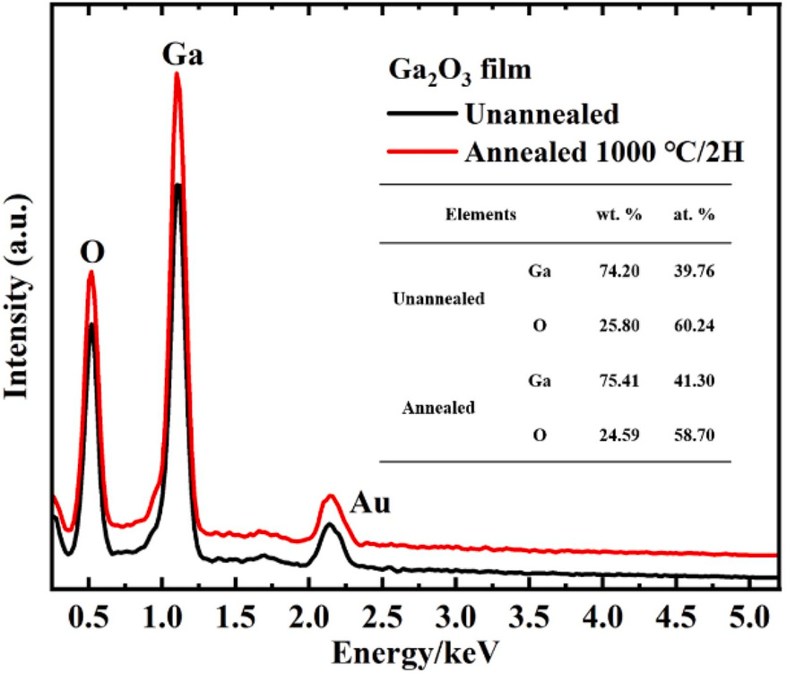
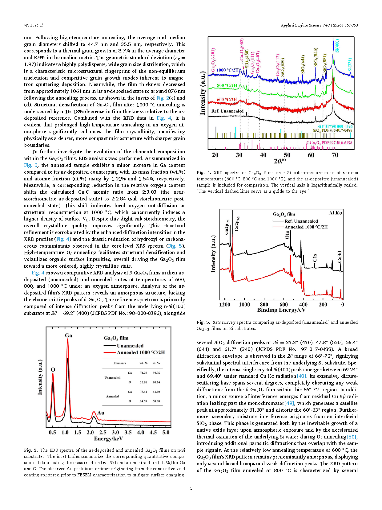
Fig. 3. The EDS spectra of the as-deposited and annealed Ga₂O₃ films on n-Si substrates. The inset tables summarize the corresponding quantitative compositional data, listing the mass fraction (wt. %) and atomic fraction (at. %) for Ga and O. The observed Au peak is an artifact originating from the conductive gold coating sputtered prior to FESEM characterization to mitigate surface charging.
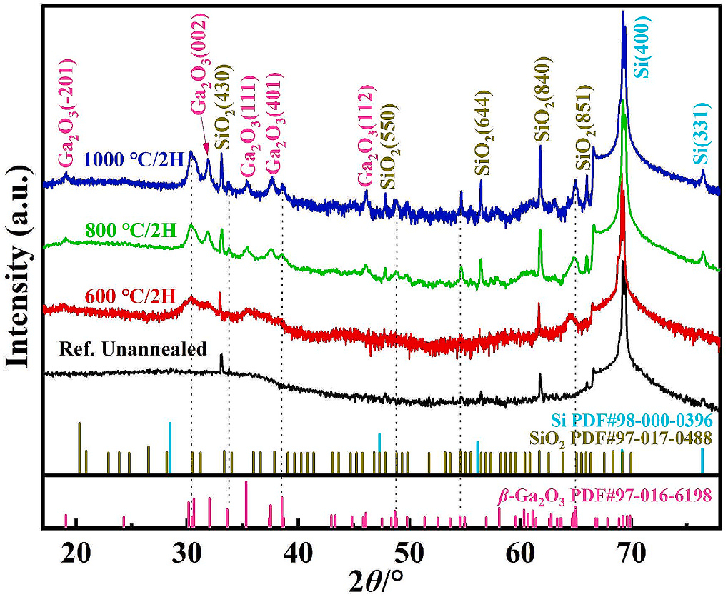
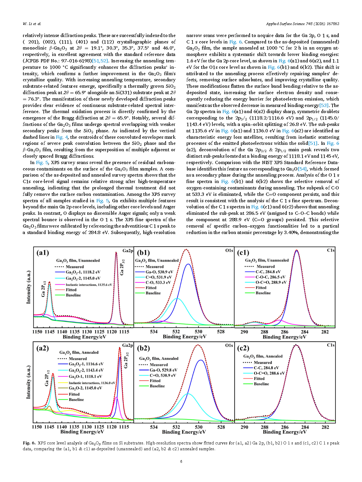
Fig. 4. XRD spectra of Ga₂O₃ films on n-Si substrates annealed at various temperatures (600 ◦C, 800 ◦C and 1000 ◦C), and the as-deposited (unannealed) sample is included for comparison. The vertical axis is logarithmically scaled. (The vertical dashed lines serve as a guide to the eye.).
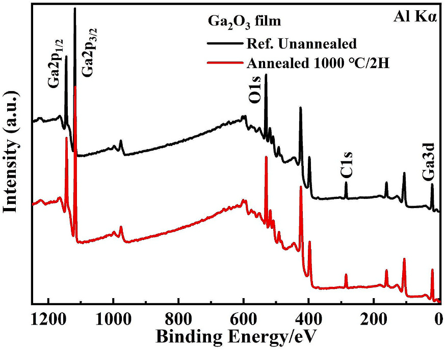
Fig. 5. XPS survey spectra comparing as-deposited (unannealed) and annealed Ga₂O₃ films on Si substrates.
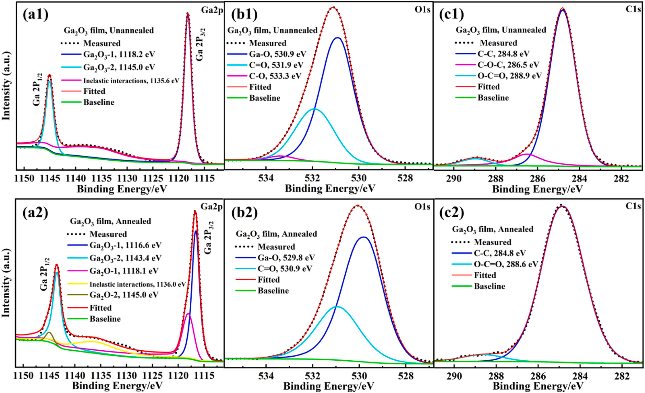
Fig. 6. XPS core level analysis of Ga₂O₃ films on Si substrates. High-resolution spectra show fitted curves for (a1, a2) Ga 2p, (b1, b2) O 1 s and (c1, c2) C 1 s peak data, comparing the (a1, b1 & c1) as-deposited and (a2, b2 & c2) annealed samples.
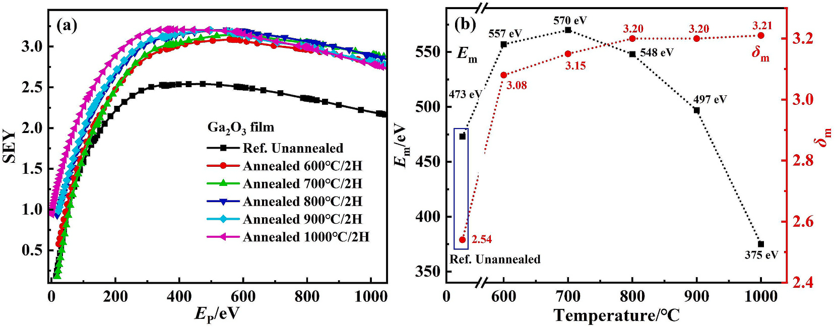
Fig. 7. SEY characteristics of Ga₂O₃ films on Si substrates. (a) SEY curves and (b) corresponding Eₘ and δₘ values are presented for samples in the as-deposited state and annealed at temperatures ranging from 600 ◦C to 1000 ◦C.
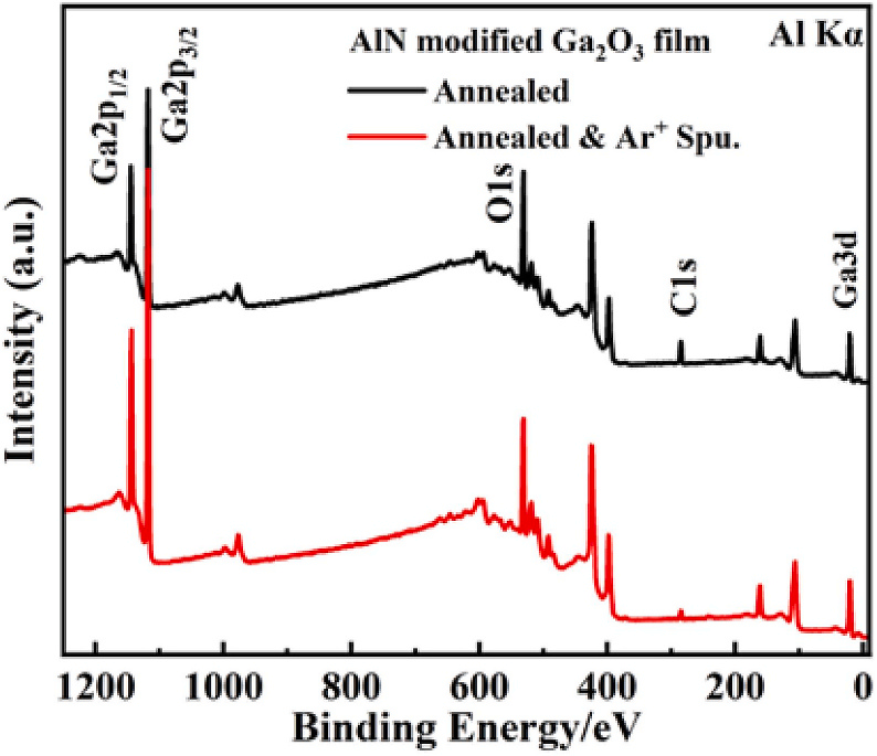
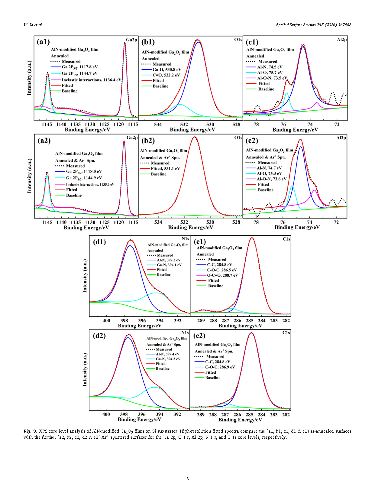
Fig. 8. XPS Survey spectra of the as-annealed AlN-modified Ga₂O₃ film, with the Ar⁺ sputtered sample shown for comparison.
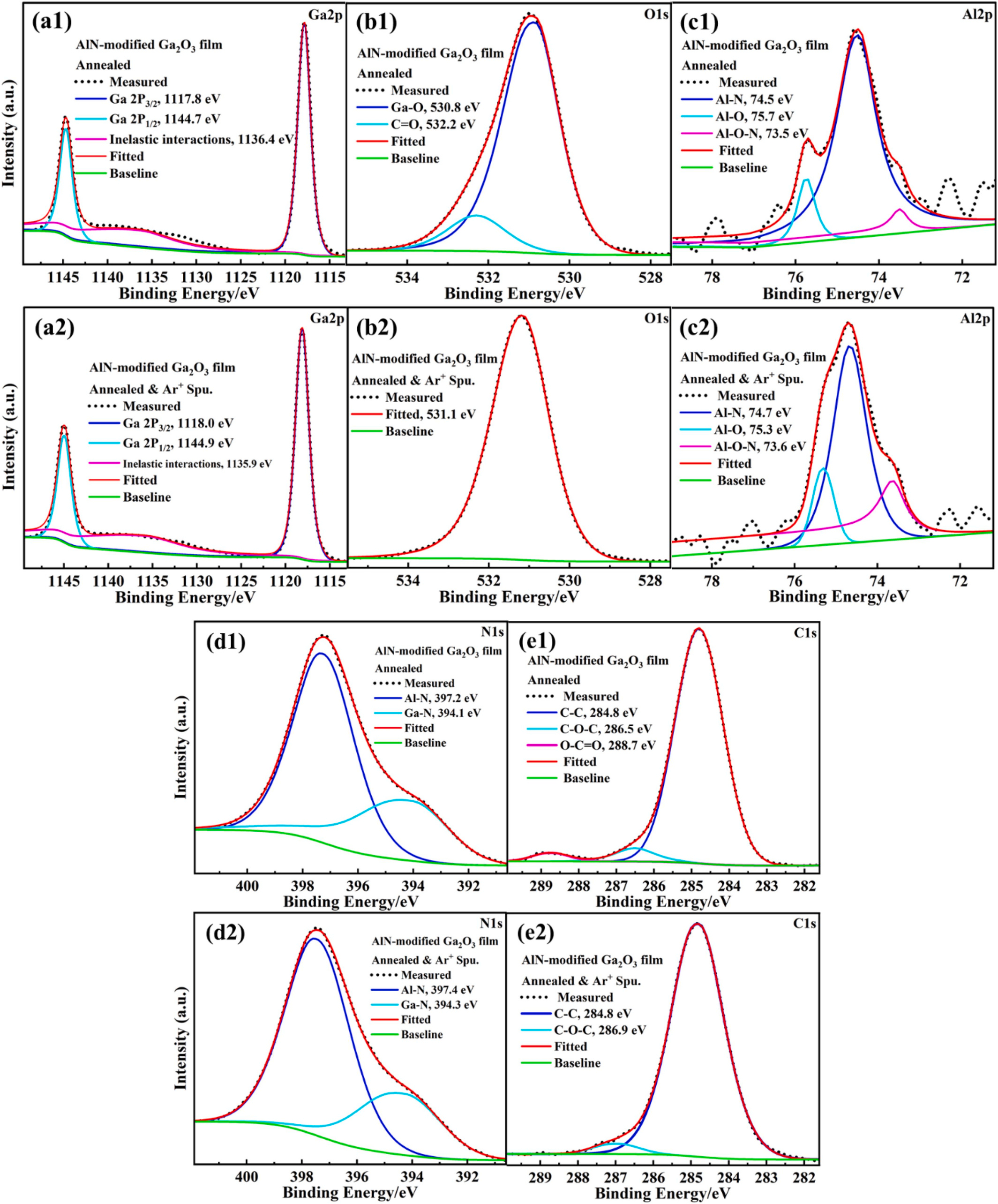
Fig. 9. XPS core level analysis of AlN-modified Ga₂O₃ films on Si substrates. High-resolution fitted spectra compare the (a1, b1, c1, d1 & e1) as-annealed surfaces with the further (a2, b2, c2, d2 & e2) Ar⁺ sputtered surfaces for the Ga 2p, O 1 s, Al 2p, N 1 s, and C 1s core levels, respectively.
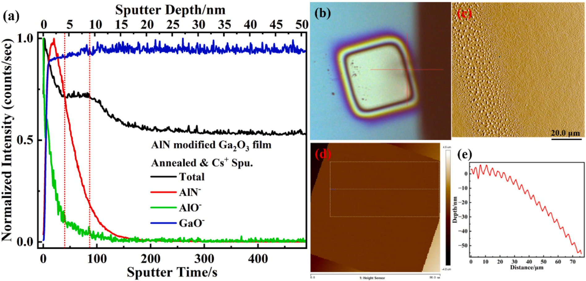
Fig. 10. (a) ToF-SIMS sputter depth profiles of the annealed AlN-modified Ga₂O₃ films, with secondary ion (SI) intensities normalized to their respective maxima. (b) Optical micrograph focusing on the edge of the Cs⁺-etched region prior to AFM characterization. (c) Morphology of the etched crater edge acquired in AFM tapping mode. (d) Selected section region (indicated by the white frame) obtained after image rotation and plan-fit processing of the AFM height image. (e) Averaged depth profile extracted in the white frame designated in (d).
DOI:
doi.org/10.1016/j.apsusc.2026.167863
Instruction
Official Account

Cooperation
Top
